
Special Issue | 02 December 2025
Special Issue on Perovskite Nanomaterials and Nanostructures Fabrication for Photonics and Optoelectronics

Metal halide perovskites stand at the nexus of materials innovation, nanoscale engineering, and real-world device integration. Their journey from laboratory curiosities to contenders for commercial photovoltaics, radiation detectors, and photocatalytic systems has been propelled not only by exceptional optoelectronic properties—but decisively, by how they are fabricated, structured, and interfaced. This Special Issue of Light: Advanced Manufacturing, titled “Perovskite Nanomaterials and Nanostructures Fabrication for Photonics and Optoelectronics”, showcases a new generation of research where synthesis, nanostructuring, and interfacial control converge to solve long-standing challenges: instability in operational environments, poor reproducibility, scalability bottlenecks, and performance ceilings.
The eight contributions featured here—selected from a competitive pool of submissions—illustrate a field in transition: from proof-of-concept demonstrations toward manufacturable, multifunctional, and mission-critical systems. Notably, the ordering of papers in this issue traces a deliberate arc—from molecular-level synthesis and colloidal control, through nanoscale patterning and heterostructure design, to device-level integration and extreme-environment resilience—reflecting the hierarchical complexity of modern perovskite engineering.
It begins at the nanoscale synthesis frontier, where Paper #1 tackles perhaps the most persistent limitation of perovskites: instability in aqueous media. By developing a one-pot hot-injection route to fabricate water-stable CsPbBr₃@TiO₂ core–shell nanocrystals—further augmented with plasmonic Au nanoparticles—the authors unlock efficient, selective solar-driven CO₂ reduction in water, achieving up to 70% Faradaic efficiency for propene (C₃H₆). This work powerfully demonstrates that nanoscale encapsulation and plasmonic coupling can jointly overcome thermodynamic and kinetic barriers, opening a pathway toward solar fuels and green chemistry.
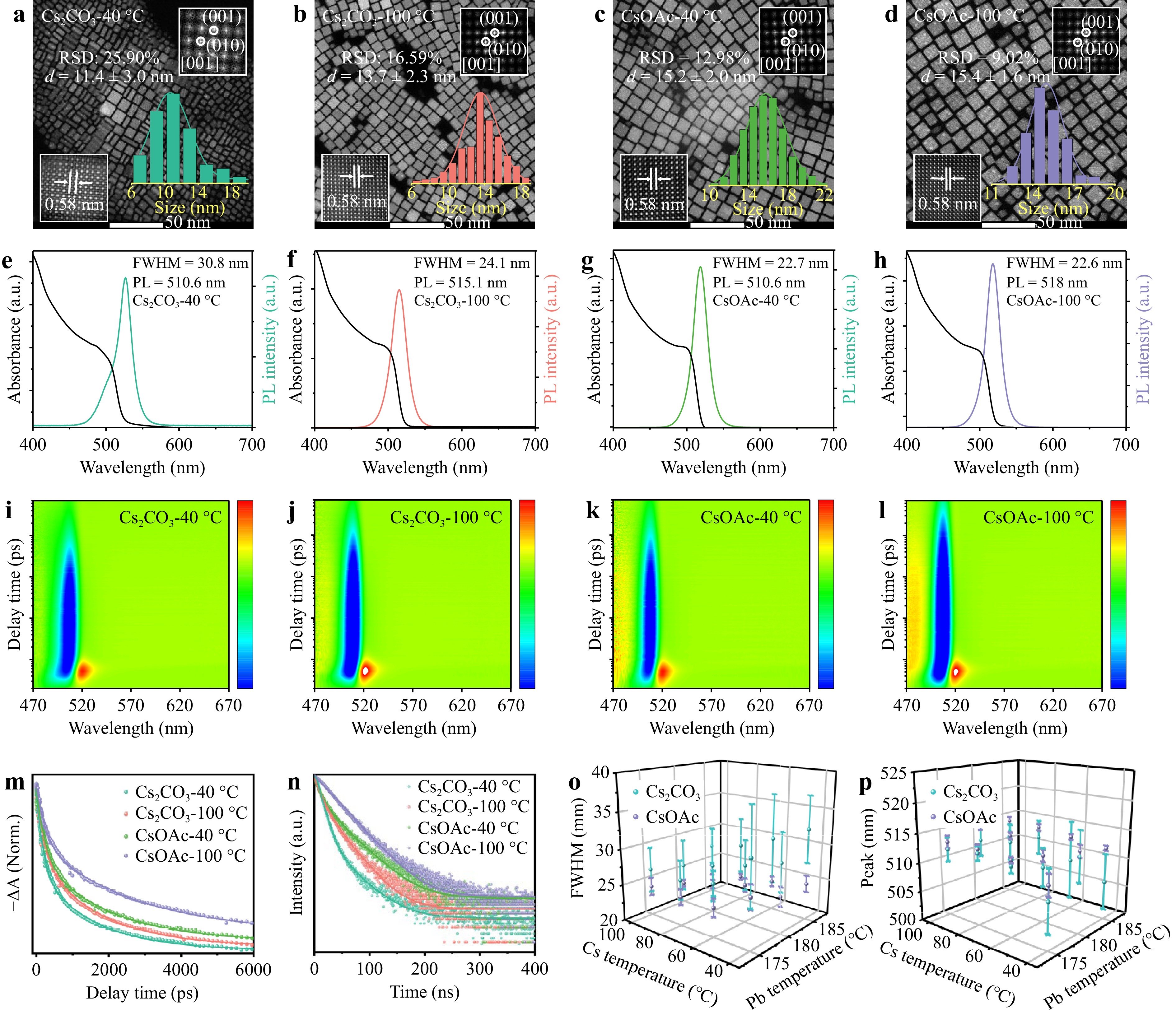
Paper #2 sharpens the focus on reproducibility and defect control in colloidal quantum dots—a longstanding pain point. Through meticulous precursor engineering (acetate + 2-hexyldecanoic acid), the authors boost cesium precursor purity from ~70% to >98%, achieving near-unity PLQY (99%), narrow emission (22 nm), and—critically—a 70% reduction in ASE threshold. This level of batch-to-batch consistency, rarely reported in perovskite QD literature, signals a maturing synthesis protocol ready for transfer to pilot-scale production.
Papers #3 and #4 pivot to top–down and bottom–up patterning, where form meets function. Paper #3 introduces a non-invasive substrate-guided nanostructuring approach: depositing perovskite films atop laser-induced periodic surface structures (LIPSS) in TiO₂. Without ablating or damaging the perovskite, this method yields structural colouration, luminescence anisotropy, and enhanced charge extraction—at a writing speed of 2.25 cm²/min, promising for roll-to-roll adoption. Complementing this, Paper #4 presents a universal dry lift-off micro-patterning technique achieving ~1 µm resolution across 100 mm wafers, and demonstrates direct integration of perovskite and CdSe QD arrays onto GaN LED chips for colour-conversion microdisplays. Together, these works bridge nanofabrication and device integration—addressing a critical gap in scalable optoelectronic manufacturing.
The middle of the issue turns to interface and bulk engineering. Paper #5 leverages the ferroelectric polymer P(VDF-TrFE) to pin the Fermi level and suppress interfacial trap states in photodiodes. The result: detectivity surpassing 10¹² Jones, 100 dB linear dynamic range, and improved thermal stability—advancing perovskite photodetectors toward parity with established technologies. Crucially, the dielectric integration preserves morphology, proving that electronic—not structural—tuning can yield transformative gains.
Papers #6 and #7 return to the wide-bandgap perovskite Cs₀.₁₇FA₀.₈₃PbI₁.₈Br₁.₂, a workhorse for perovskite/Si tandems. Paper #6 applies bi-solvent engineering to achieve not only lab-scale efficiency gains but—remarkably—a 10% efficient 25 cm² mini-module using acetonitrile-based processing: a significant step toward manufacturability. Paper #7 then subjects the same composition to γ-ray irradiation, uncovering a surprising defect-passivation mechanism at doses ≤10 kGy, enabling radiation-hardened solar cells. These complementary studies underscore that processing and environmental response must be co-optimized—especially for space or nuclear applications.
Finally, Paper #8 closes the issue on a forward-looking, application-driven note: a lead-free, flexible X-ray scintillator based on a novel 0D cuprous halide, (MTP)₂Cu₄I₆. With near-unity PLQY (99.9%), negligible self-absorption, sub-µs response, and 10.2 lp mm⁻¹ resolution in PDMS films, this material challenges the dominance of toxic or brittle alternatives in medical and security imaging. Its success exemplifies how perovskite-inspired (though not perovskite-structured) materials can fulfill real-world safety and performance requirements—expanding the field’s impact beyond classical device architectures.
Collectively, these papers embody a maturing discipline. Where early perovskite research emphasized composition space and record efficiencies, today’s frontier lies in fabrication control—across length scales, from atomic ligands to wafer-scale patterning; across environments, from ambient air to ionizing radiation; and across applications, from microdisplays to carbon-neutral fuel synthesis.
We extend our deepest gratitude to the authors for their rigor and vision, to the reviewers for their incisive feedback, and to the editorial team of Light: Advanced Manufacturing for their support.
This issue is co-edited by
Prof. Sergey Makarov, Harbin Engineering University, China & ITMO University, Russia
Dr. Emmanuel Stratakis, Institute of Electronic structure and laser (IESL) of the Foundation for Research and Technology-Hellas(FORTH), Greece
Prof. Nikolay V. Petrov,ITMO University, Russia
-
Editorial
Perovskite nanomaterials and nanostructures manufacturing: from atomic to wafer scale engineering
-
Article
Heterostructured perovskite nanocrystals for water stable plasmon-enhanced photoelectrocatalysis
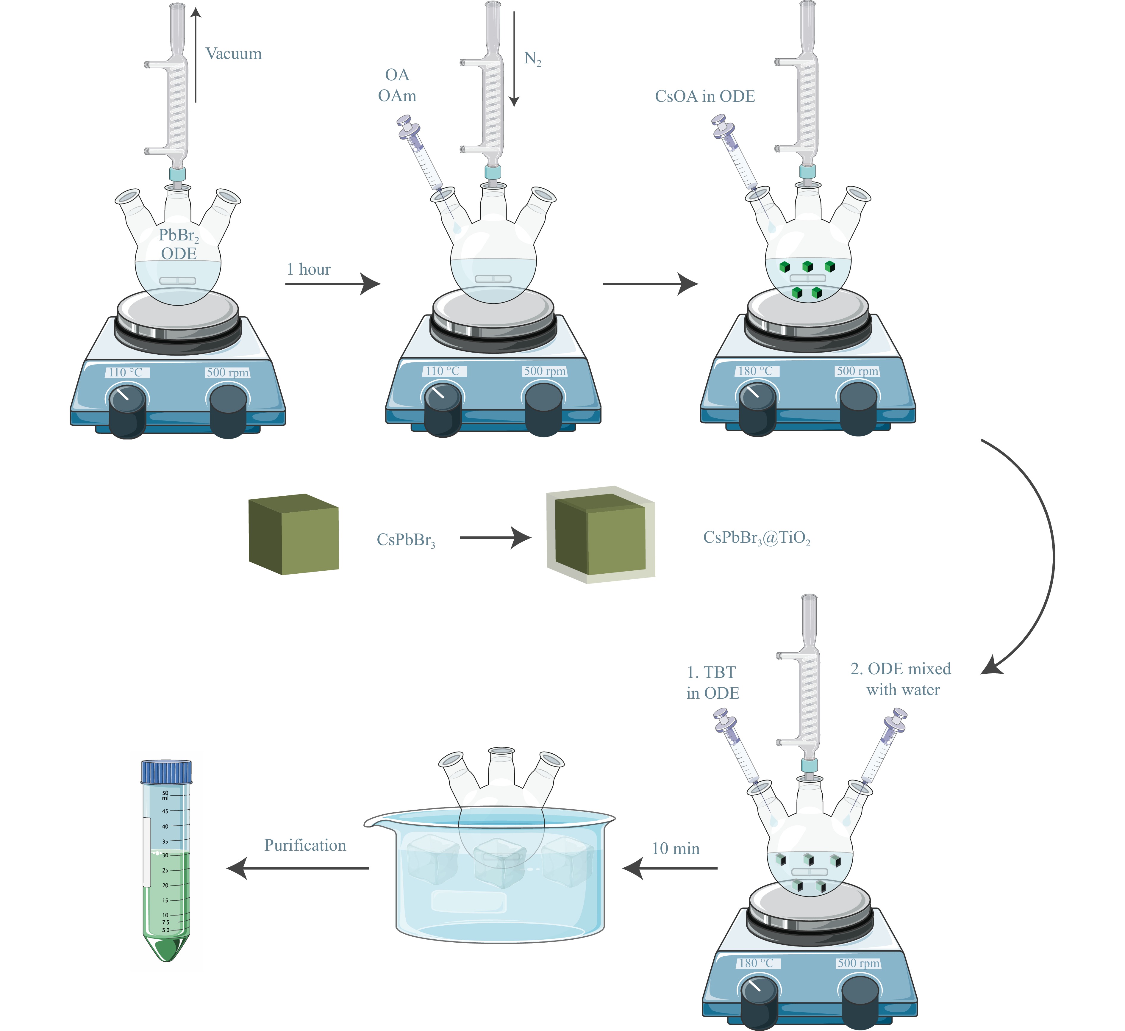 Published , Published online: 25 November 2025 , doi: 10.37188/lam.2025.080Perovskite photoelectrocatalysis enables solar-driven conversion of CO2 to value-added chemicals, but instability in water and insufficient C–C coupling still constrain performance. Herein, we present a synergistic approach for aqueous-phase CO2 conversion that combines perovskite-based photoelectrocatalysis with localized surface plasmon resonance (LSPR) enhancement. To address the inherent instability of lead-halide perovskites, we developed a modified hot-injection route that enables the in situ formation of water-stable CsPbBr3@TiO2 core–shell nanoparticles. Titanium butoxide and water were introduced after Cs-oleate injection, enabling controlled TiO2 shell growth without post-treatment. Electron microscopy, XRD, and XPS confirm the core–shell architecture, while optical/electrical probes indicate efficient charge separation across the CsPbBr3/TiO2 junction. Subsequently, we investigated electrocatalytic, photocatalytic, and photoelectrochemical carbon dioxide reduction (CO2RR) on CsPbBr3@TiO2/Au and CsPbBr3@TiO2. Gas chromatography revealed tunable product selectivity, yielding H2, CO, CH4, and multicarbon (C2, C3) products including C2H4 (ethylene) and C3H6 (propene). Our main findings indicate that the CsPbBr3@TiO2/Au exhibits high selectivity toward C3 (propene) in photocatalysis and C2 (ethylene) in photoelectrochemistry, reaching up to 70% and 58%, respectively. These results highlight perovskite heterostructures as a viable platform for efficient CO2 utilization and the sustainable production of value-added C2/C3 chemicals.
 -
Article
High-quality perovskite quantum dots with excellent reproducibility and amplified spontaneous emission by optimization of cesium precursor
 Published , Published online: 05 March 2025 , doi: 10.37188/lam.2025.012
Lead halide perovskite quantum dots (QDs) suffer from frequent batch-to-batch inconsistencies and poor reproducibility, resulting in serious non-radiative defect-assisted recombination and Auger recombination. To overcome these challenges, in this study, CsPbBr3 QDs were prepared by designing a novel cesium precursor recipe that involved a combination of dual-functional acetate (AcO−) and 2-hexyldecanoic acid (2-HA) as short-branched-chain ligand: first, AcO− aided in significantly improving the complete conversion degree of cesium salt, enhancing the purity of the cesium precursor from 70.26% to 98.59% with a low relative standard deviation of size distribution and photoluminescence quantum yield (9.02 and 0.82%, respectively) by decreasing the formation of by-products during the reaction, which leads to enhanced homogeneity and reproducibility, especially at room temperature. Second, AcO− can act as a surface ligand to passivate the dangling surface bonds. Furthermore, compared to oleic acid, 2-HA exhibited a stronger binding affinity toward the QDs, further passivated the surface defects, and effectively suppressed biexciton Auger recombination, thereby improving the spontaneous emission rate of the QDs. Consequently, the QDs prepared using this new recipe exhibited a uniform size distribution, a green emission peak at 512 nm, a high photoluminescence quantum yield of 99% with excellent stability, and a narrow emission linewidth of 22 nm. In particular, the optimized QDs exhibited enhanced amplified spontaneous emission (ASE) performance, while the ASE threshold of treated QDs reduced by 70% from 1.8 μJ·cm−2 to 0.54 μJ·cm−2.
-
Article
Structural colouring and luminescence anisotropy of perovskite thin films via laser-induced periodic surface structure formation
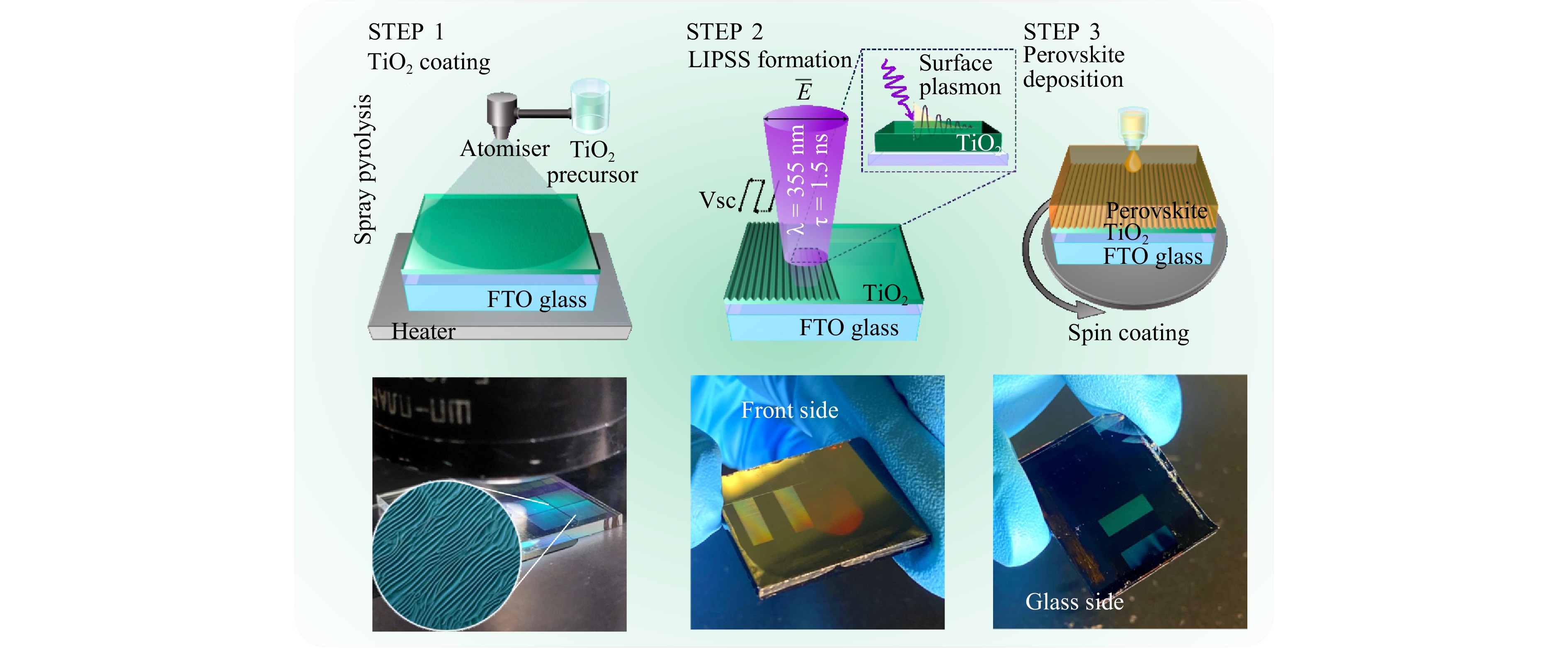 Published , Published online: 22 September 2025 , doi: 10.37188/lam.2025.062Perovskite nanostructured films are essential to create advanced optoelectronic and photovoltaic devices because of the additional degrees of freedom of manipulation by light reflection and structural colouration, as well as by light trapping and localisation, resulting in control of intensity or polarisation of luminescence. In this paper, we report structural colouration and photoluminescence anisotropy in perovskite films deposited on a substrate with laser-induced periodic surface structures (LIPSSs) on a thin TiO2 layer. The LIPSS TiO2 layer improves charge extraction from the perovskite films, confirmed by a time-resolved photoluminescence analysis. The developed method of substrate nanostructuring does not damage the perovskite films, in contrast to direct laser ablation, imprinting by a mould, mechanical scratching with a cantilever, or plasma-chemical etching. Moreover, the LIPSS formation is appropriate for upscaling owing to the high speed of LIPSS writing (2.25 cm2min-1) and uniform surface nanostructuring.
 -
Article
A universal high-resolution micro-patterning technique for solution-processed materials
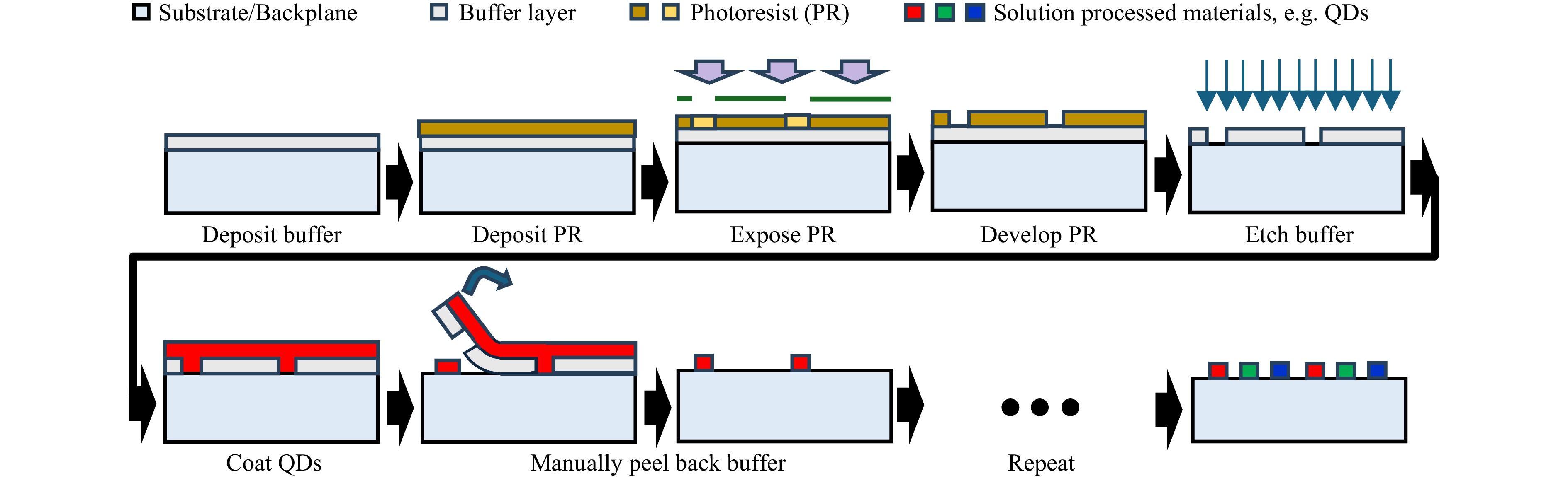 Published , Published online: 19 March 2025 , doi: 10.37188/lam.2025.015A universal method of micro-patterning thin quantum dot films is highly desired by industry to enable the integration of quantum dot materials with optoelectronic devices. Many of the methods reported so far, including specially engineered photoresist or ink-jet printing, are either of poor yield, resolution limited, difficult to scale for mass production, overly expensive, or sacrificing some optical quality of the quantum dots. In our previous work, we presented a dry photolithographic lift-off method for pixelization of solution-processed materials and demonstrated its application in patterning perovskite quantum dot pixels, 10 µm in diameter, to construct a static micro-display. This report presents further development of this method and demonstrates high-resolution patterning (~1 µm diameter), full-scale processing on a 100 mm wafer, and multi-color integration of two different varieties of quantum dots. Perovskite and cadmium-selenide quantum dots were adopted for the experimentation, but the method can be applied to other types of solution-processed materials. We also demonstrate the viability of this method for constructing high-resolution micro-arrays of quantum dot color-convertors by fabricating patterned films directly on top of a blue gallium-nitride LED substrate. The green perovskite quantum dots used for fabrication were synthesized via the room-temperature ligand-assisted reprecipitation method developed by our research group, yielding a photoluminescent quantum yield of 93.6% and full-width half-maximum emission linewidth less than 20 nm. Our results demonstrate the viability of this method for use in scalable manufacturing of high-resolution micro-displays paving the way for improved optoelectronic applications.
 -
Article
Improvement of the perovskite photodiodes performance via advanced interface engineering with polymer dielectric
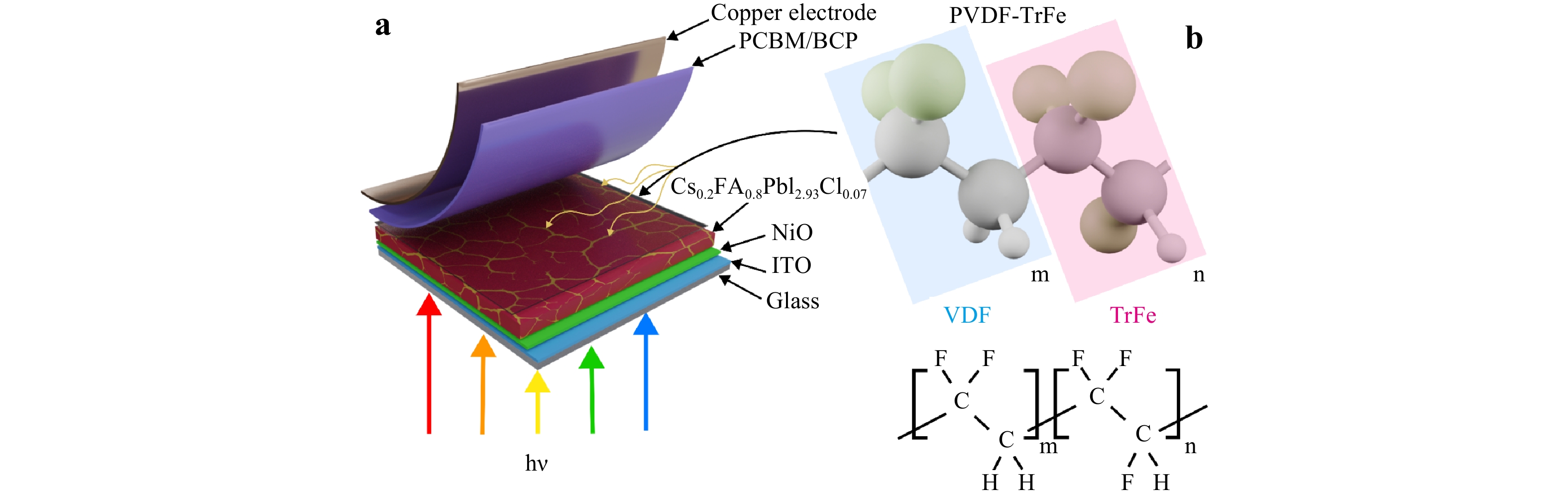 Published , Published online: 18 March 2025 , doi: 10.37188/lam.2025.024
Halide perovskite-based photodiodes are promising for efficient detection across a broad spectral range. Perovskite absorber thin-films have a microcrystalline morphology, characterized by a high density of surface states and defects at inter-grain interfaces. In this work, we used dielectric/ferroelectric poly(vinylidene-fluoride-trifluoroethylene) (P(VDF-TrFE)) to modify the bulk interfaces and electron transport junction in p-i-n perovskite photodiodes. Our complex work demonstrates that interface engineering with P(VDF-TrFE) induces significant Fermi level pinning, reducing from 4.85 eV for intrinsic perovskite to 4.28 eV for the configuration with dielectric interlayers. Modifying the interfaces in the devices resulted in an increase in the key characteristics of photodiodes compared to pristine devices. The integration of P(VDF-TrFE) into the perovskite film didn’t affect the morphology and crystal structure, but significantly changed the charge transport and device performance. IV curve analysis and 2-diode model calculations showed enhanced shunt properties, a decreased non-ideality factor, and reduced saturation dark current. We have shown that the complex introduction of P(VDF-TrFE) into the absorber’s bulk and on its surface is essential to reduce the impact of the trapping processes. For P(VDF-TrFE) containing devices, we increased the specific detectivity from 1011 to ~1012 Jones, expanded the linear dynamic range up to 100 dB, and reduced the equivalent noise power to 10−13 W·Hz−1/2. Reducing non-radiative recombination contributions significantly enhanced device performance, improving rise/fall times from 6.3/10.9 µs to 4.6/6.5 µs, and achieved photo-response dynamics competitive with state-of-the-art analogs. The cut-off frequency (3dB) increased from 64.8 kHz to 74.8 kHz following the introduction of the dielectric. We also demonstrated long-term stabilization of PPD performance under heat-stress. These results provide new insights into the use of organic dielectrics and an improved understanding of trap-states/ion defect compensation for detectors based on perovskite heterostructures.
-
Article
Enhancing the MA-free mixed halide perovskite efficiency and stability through bi-solvent engineering approach
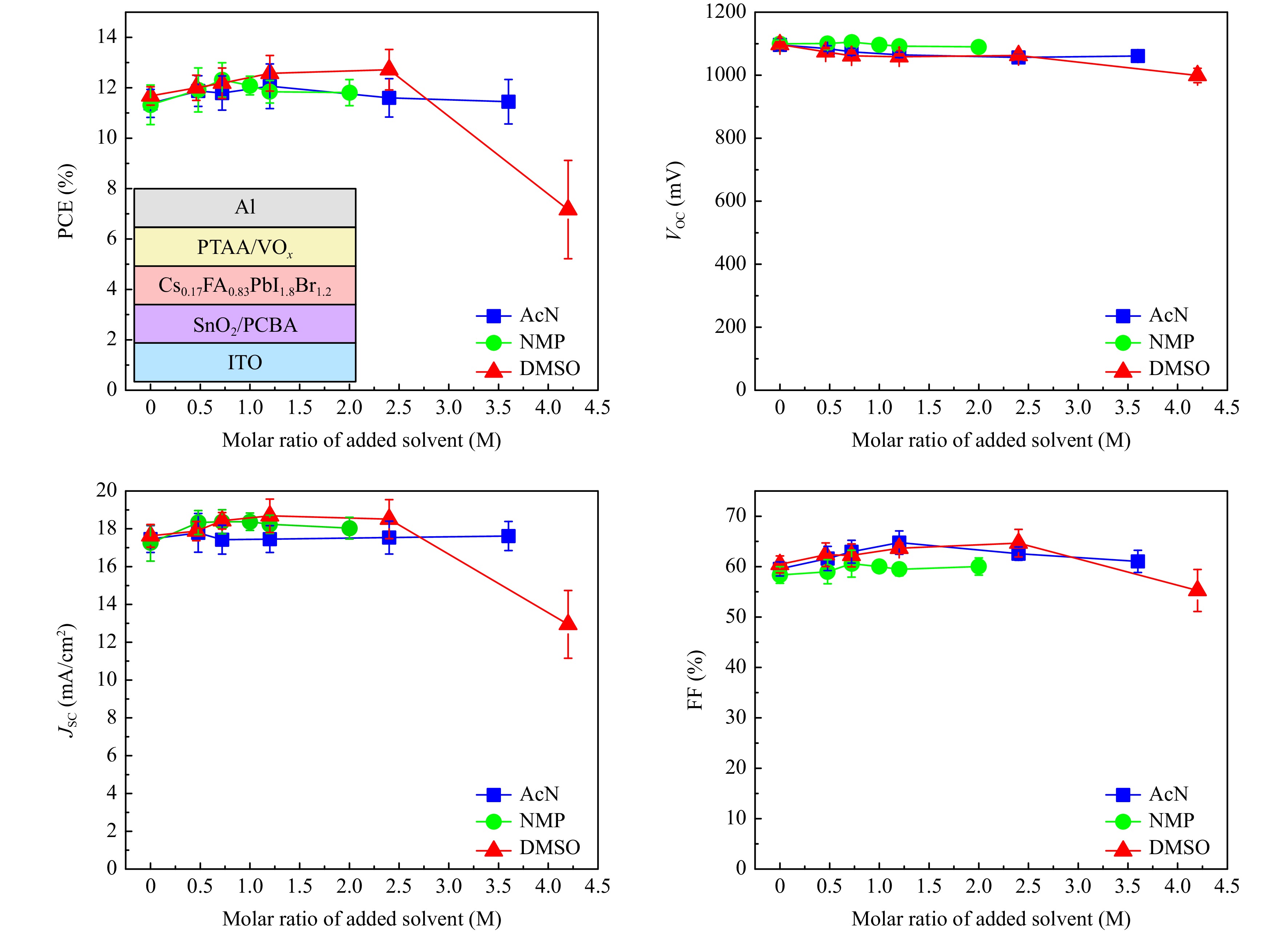 Published , Published online: 25 July 2025 , doi: 10.37188/lam.2025.039Perovskite photovoltaics upholds the most prominent position in the field of tandem technology development. In this aspect, the creation of perovskite material with suitable bandgap (≥ 1.65 eV) is necessary. And in order to achieve the best device characteristics, the high-quality film formation is crucial. To get a high-quality film, the solvent engineering approach stays at the forefront. However, although the solvent engineering was well discussed for such conventional material as MAPbI3, the field of wide bandgap perovskite materials is still lacking in this area. This paper presents the solvent engineering approach to improve the efficiency and stability of the conventional wide bandgap perovskite material Cs0.17FA0.83PbI1.8Br1.2. Here we utilize several solvents such as traditional N,N-dimethylformamide, dimethyl sulfoxide, N-methyl-2-pyrrolidone and acetonitrile. It was demonstrated that implication of any binary DMF-X solvent improves the solar cell efficiency compared to the pure DMF solution, but the ratio of the X solvent is unique for every X and the foundation for the X influence is also unique. The addition of 2.4 M of DMSO is considered the best to improve the stability and efficiency of laboratory devices, however implementation of AcN allowed to produce 25 cm2 mini-modules with the PCE reaching 10%.
 -
Article
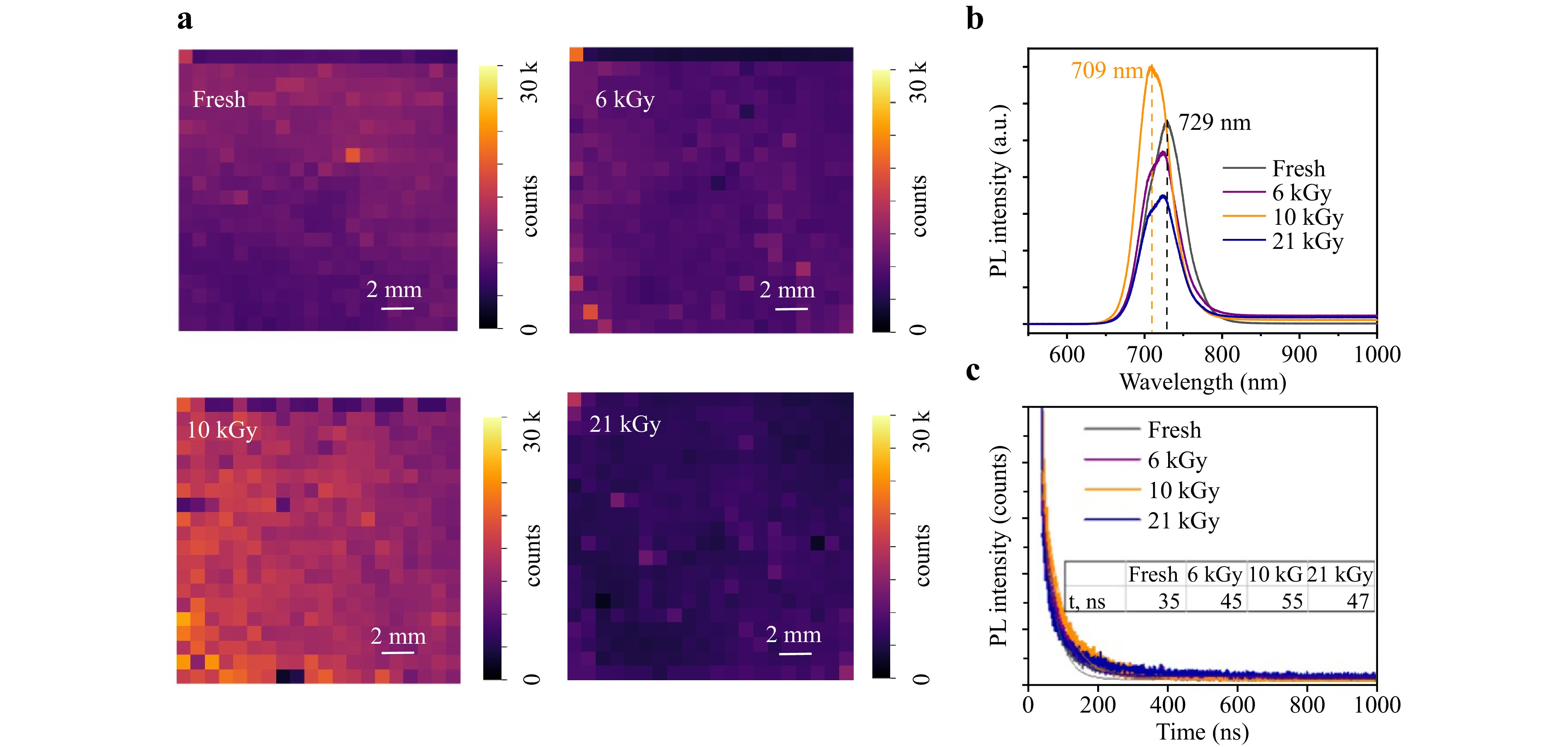
Effect of gamma-rays on recombination dynamics and defect concentration in a wide bandgap perovskite
 Published , Published online: 19 December 2024 , doi: 10.37188/lam.2024.053
Herein, we have explored the recombination dynamics and defect concentration of a mixed cation mixed halide perovskite Cs0.17FA0.83PbI1.8Br1.2 with 1.75 eV bandgap after exposure to a gamma-ray source (2.5 Gy/min). We used photoluminescent spectroscopy to observe changes in recombination dynamics on perovskite films, impedance spectroscopy to reveal the contribution of interface recombination, and admittance spectroscopy to define the activation energy and concentration of defects. It was revealed that moderate doses (up to 10 kGy) passivate defects with activation energy ≈ 0.5 eV and at the same time form new defects that cause dramatic growth of the diffusion coefficient and migration of mobile ions. These two processes with opposite direction result in high radiation tolerance of the studied material and solar cells up to 10 kGy. Doses above 10 kGy are detrimental for perovskite solar cells, mainly due to the growing role of interface recombination. The results encourage the use of the wide bandgap perovskite Cs0.17FA0.83PbI1.8Br1.2 as a material for tandem solar cells with potential applications in a space environment.
-
Article
Large-area, high-resolution, flexible x-ray scintillator film based on a novel 0d hybrid cuprous halide
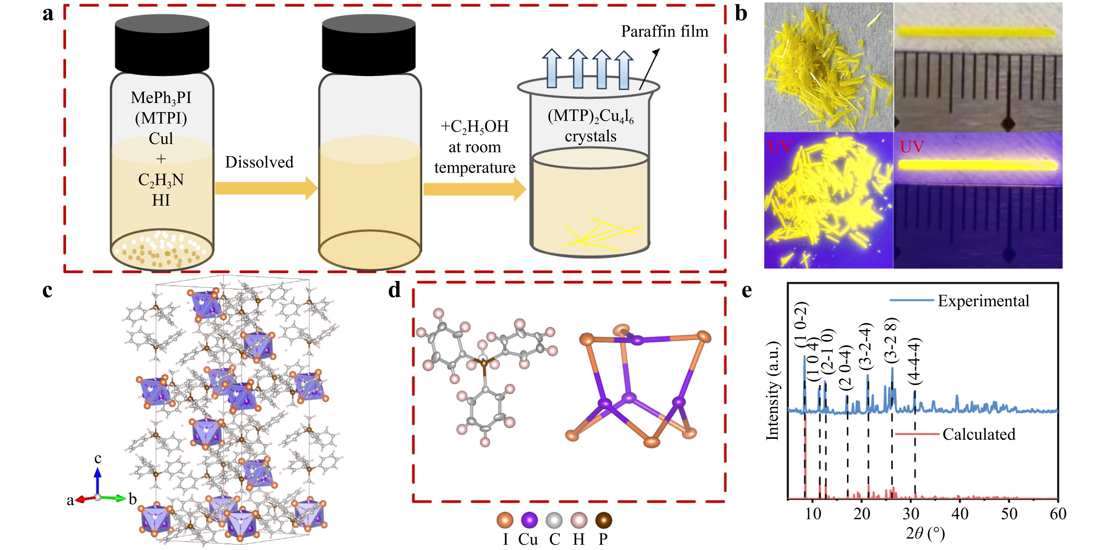 Published , Published online: 30 October 2025 , doi: 10.37188/lam.2025.044X-ray scintillation detectors play an irreplaceable role in medical imaging, security inspections, and nondestructive detection. Recently, all-inorganic lead-free metal halide scintillators have attracted attention for addressing the drawbacks of lead-halide perovskites, such as severe self-absorption and toxicity. Nevertheless, high-resolution, flexible, and cost-effective lead-free scintillators are desirable for X-ray imaging applications. In this study, we designed a zero-dimensional hybrid cuprous halide, (MTP)2Cu4I6 (MTP+ represents [C19H18P]+), and synthesized single crystals. (MTP)2Cu4I6 shows intense yellow emission (618 nm) and a large Stokes shift of 185 nm, almost eliminating the effect of self-absorption. As a result, (MTP)2Cu4I6 exhibited a near-unity photoluminescence quantum yield (99.9%) with a light yield of 43800 photons per megaelectron volt. Moreover, (MTP)2Cu4I6 demonstrates an impressive detection performance with a fast response time of 2.18 μs, a good linear response ranging from 0.038 μGyair s−1 to 53.4 μGyair s−1, and a low detection limit of 37.6 nGyair s−1. In a conceptual experiment, large-area flexible (MTP)2Cu4I6/polydimethylsiloxane (PDMS) scintillation films were fabricated to investigate their X-ray imaging performance. The (MTP)2Cu4I6/PDMS film exhibits a high-spatial resolution of 10.2 lp mm−1 when the modulation transfer function is 0.2 and superior flexible detection performance. The short lifetime, high-light yield, low toxicity, and low cost of (MTP)2Cu4I6 facilitate the development of next-generation X-ray scintillators.

Sergey Makarov is a Professor of Harbin Engineering University and ITMO University. He is a co-author of more than 300 publications and 20 patents. The topics of his research activity include nanophotonics, halide perovskites, laser-matter interaction, nanotechnology, and optoelectronics. He won “Research Excellence Award” from Elsevier, grant for International Excellent Young Scientists NSFC, Presidential Award, and many other awards.

Emmanuel Stratakis is a Research Director at the Foundation of Research and Technology Hellas. He is a co-author of more than 270 publications and 8 patents. The topics of his research activity include Ultrashort pulsed laser-matter interaction, biomimetics. nanotechnology and nanophotonics. He is an expert in the High-Level Group of EU on Nanotechnologies, He is an OPTICA Fellow and Ambassador of the European Innovation Council. He is the founder and CEO of Biomimetic.

Nikolay V. Petrov received a master's degree from Saint-Petersburg State University in 2007 and got a Ph.D. degree in optics from the ITMO University, St. Petersburg, Russia. Since 2011, he has been a Senior Researcher and Associate Professor with the Department of Photonics and Optical Information Technology, ITMO University. Since 2016 he established a digital and display holography laboratory, and since 2017 he is a leading researcher. In 2019 he gained a doctorate (Dr. habil.) degree in optics. His research interests are currently focused on holography, femtosecond optics, and terahertz imaging. He has co-authored around 100 publications in the Scopus database. He is a member of OSA, SPIE and the Optical Society named after D.S. Rozhdestvensky. Dr. Petrov was the recipient of the Russian Federation Government Prize in Education in 2010 and is a winner of several prizes: St. Petersburg Youth Award in Education in 2012, Yu. I. Ostrovsky Prizes for the best scientific work in the field of optical holography and interferometry in 2012, and 2015, St. Petersburg Government Prize in the field of scientific and pedagogical activity in 2015 and Yu.N. Denisyuk medal in 2017. OSA Senior Member from 2019.

 Email
Email RSS
RSS