
View by Category
Published
, Published online: 29 July 2026
, doi: 10.37188/lam.2026.022
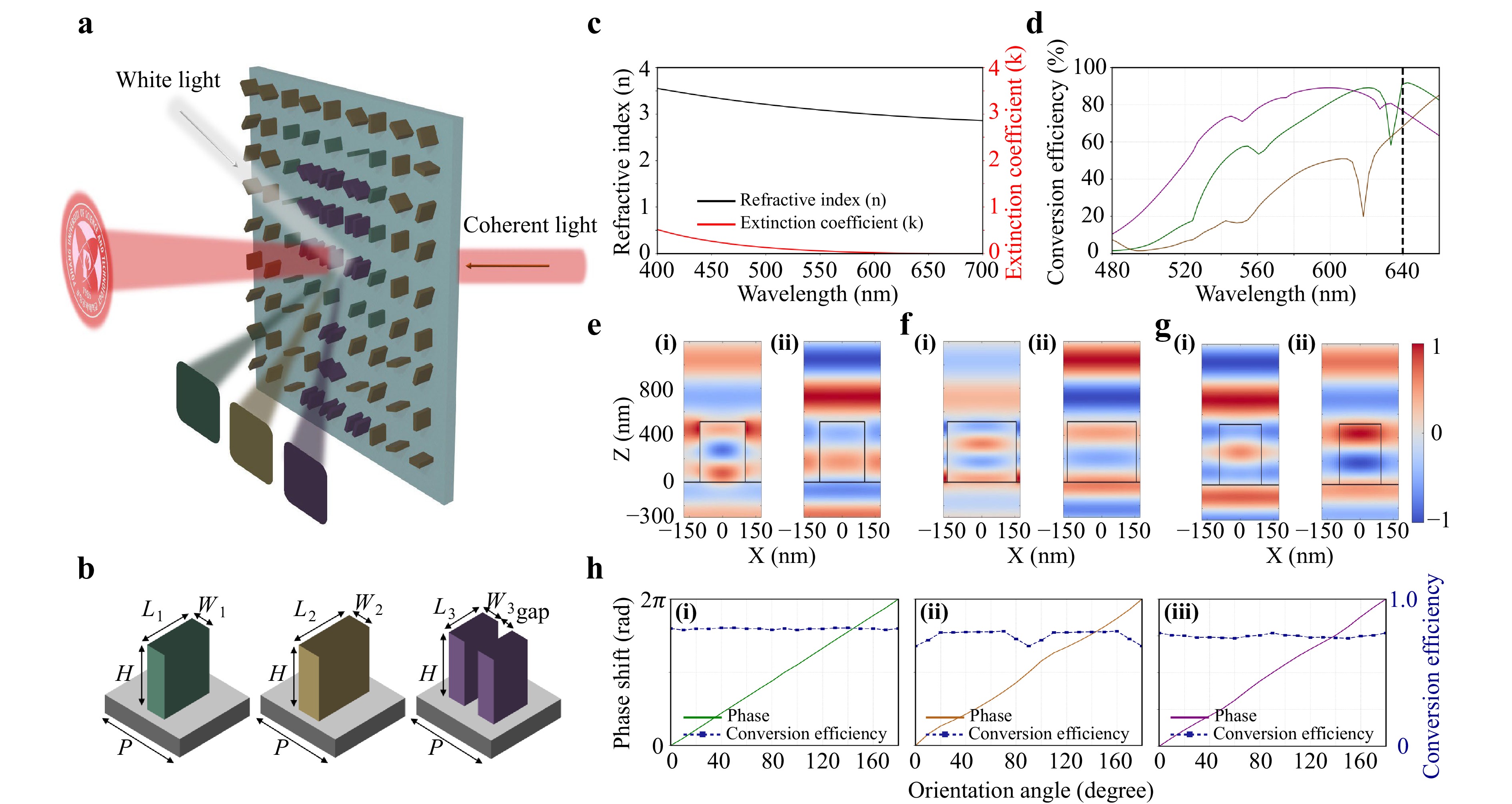
Metasurfaces, flat optical devices built from nanoscale structures, offer powerful and precise control over light. They have enabled applications such as structural color printing by manipulating spectral responses and holography through precise phase control. Integrating these functions into a single metasurface has gained interest for compact multifunctional platforms. However, most existing dual-mode designs suffer from low hologram efficiency, limiting their practical applications in multifunctional optical systems. Here, we present dual-functional metasurfaces that simultaneously enable three-color structural printing under white light illumination and high-efficiency holography under coherent light. Our design employs three distinct meta-atoms, composed of single and double nanorods, to achieve independent spectral and phase modulations. The metasurfaces produce three distinct reflective colors of green, brown, and magenta and achieve numerical conversion efficiency up to 90% at the 640 nm wavelength. The fabricated devices successfully display desired structural colors under white light and reconstruct holographic images with high efficiency under coherent illumination. The devices also demonstrate broadband performance for holography across the visible spectrum. These results confirm the effectiveness of our design in achieving independent and efficient control of color and holography within a single metasurface. This multifunctional capability offers strong potential for applications in anti-counterfeiting and compact optical data storage.


Published
, Published online: 24 July 2026
, doi: 10.37188/lam.2026.086
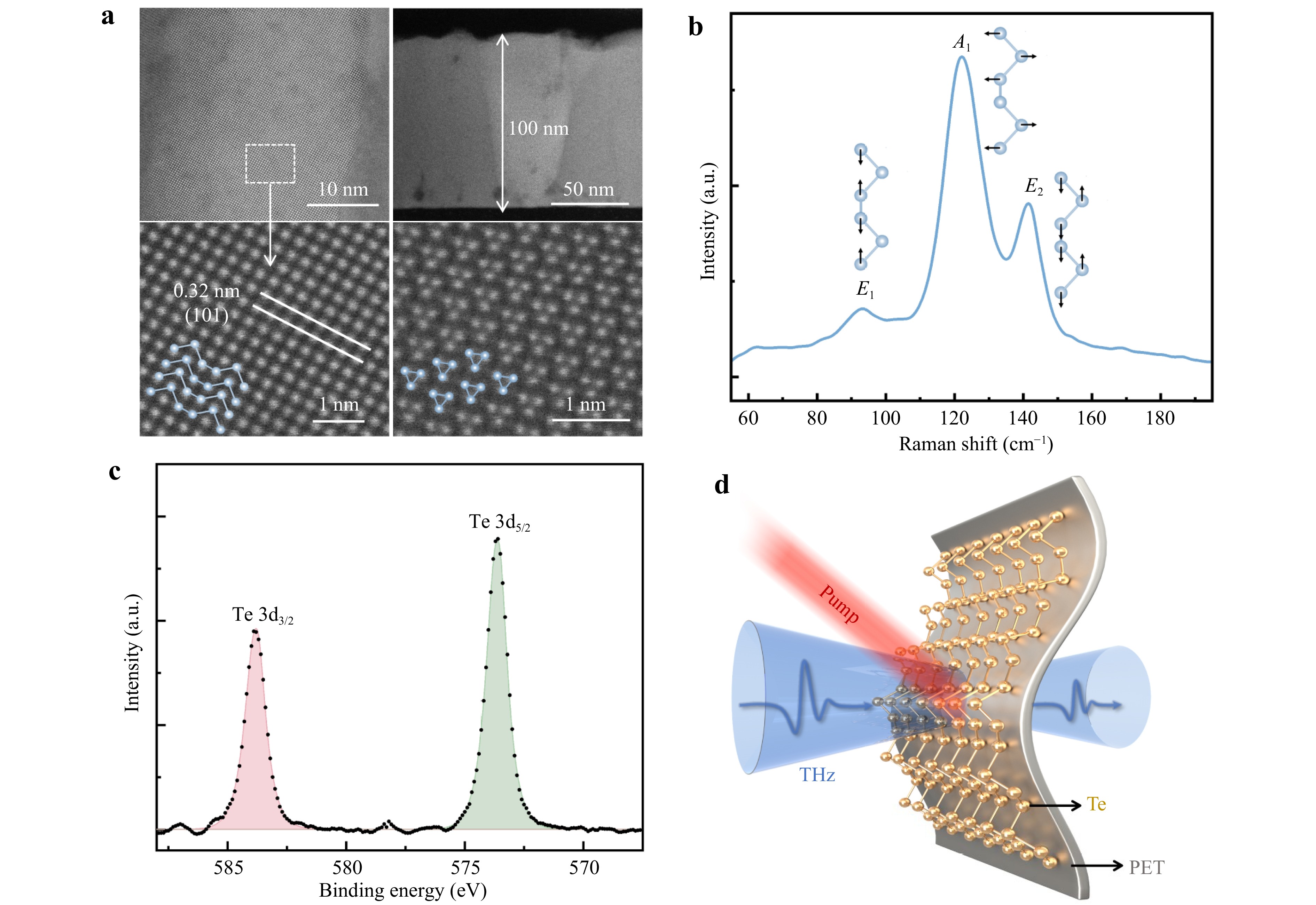
Flexible terahertz (THz) devices are fundamental components of wearable photonics and intelligent communication systems. However, conventional THz devices are affected by information loss or signal interruption due to mechanical deformation, which degrade their information fidelity. Here, we introduce tellurium (Te) nanofilms grown on polyethylene terephthalate (PET) substrates as a new class of mechanically robust THz modulators that can successfully improve device performances to optimal levels among existing flexible broadband modulators. The ultrafast transient THz photoresponses of two-dimensional Te films remained unchanged even after 1000 bending cycles or at a small bending radius of 3 mm, exhibiting high tolerance to bending deformation. Furthermore, the variations in the pattern recognition accuracy remained within 2% under different bending conditions, indicating its adaptability to various deformation conditions. This prototype lays the foundation for developing intelligent perception elements that operate stably under complex mechanical deformations.


Published
, Published online: 22 July 2026
, doi: 10.37188/lam.2026.075
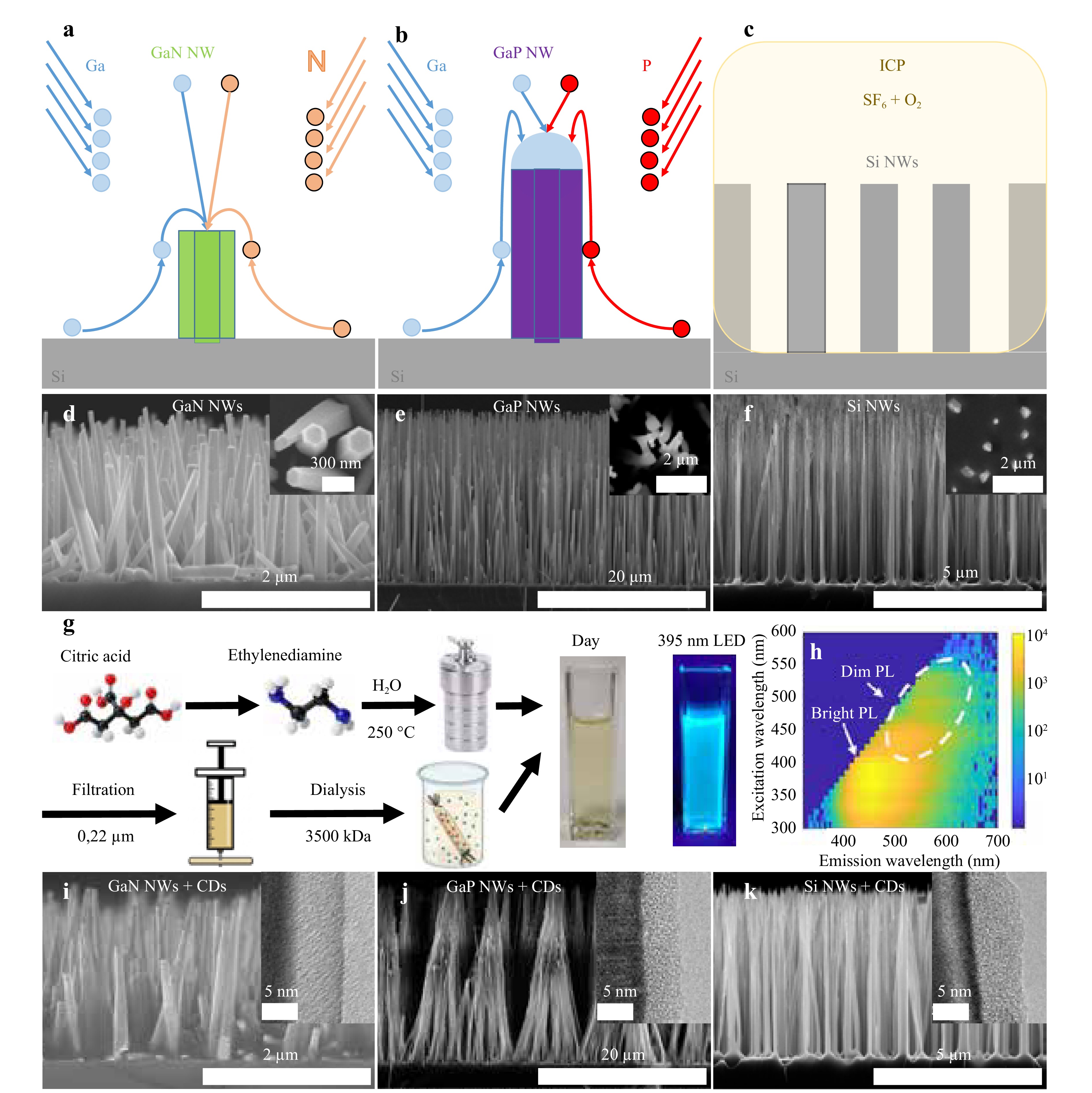
The integration of luminescent nanomaterials into scalable semiconductor platforms is vital for on-chip photonics. This study demonstrates an approach to fabricate fluorescent nanostructures by hybridising carbon dots (CDs) with semiconductor nanowires (NWs) grown on Si. We systematically investigated the photoluminescence of CDs on GaN, GaP, and Si NW hosts and demonstrated the key role of the absorption edge of the host as a practical spectral filter. Our results show that efficient CD excitation is governed by the transparency window of the NW, thereby allowing the precise tailoring of the emission spectrum through rational host selection. This effect has been consistently demonstrated in different materials. By coupling the tuneable chemistry of CDs with the tailored optoelectronics of semiconductor NWs, this study establishes a scalable host-guest architecture for engineering nanoscale light sources to promote applications in integrated photonic circuits and sensing.


Published
, Published online: 22 July 2026
, doi: 10.37188/lam.2026.098
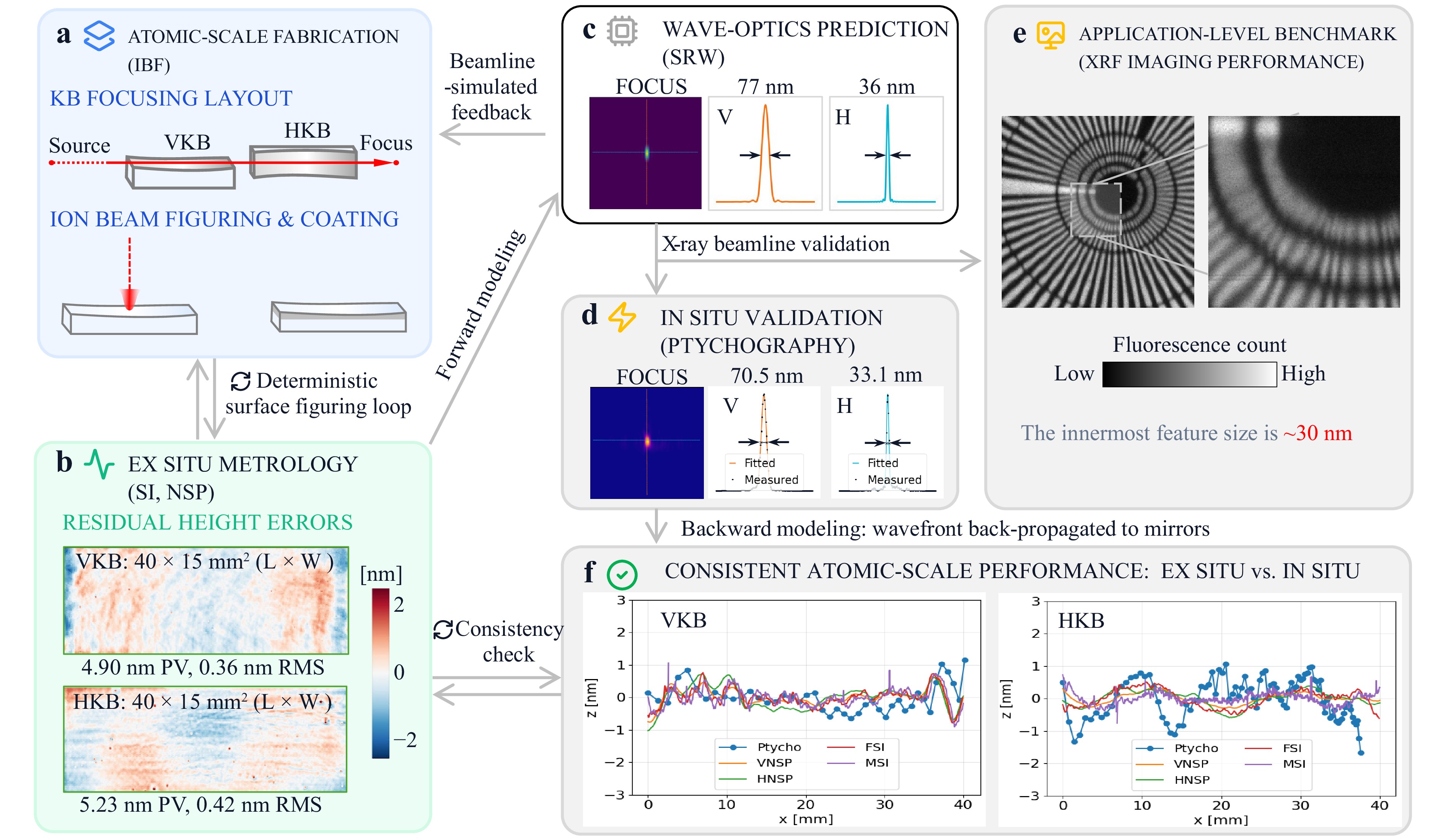
Diffraction-limited synchrotron sources place stringent demands on wavefront-preserving X-ray optics. We report a fully in-house, closed-loop pipeline at the National Synchrotron Light Source II that links ion beam figuring, precision ex situ metrology, wavefront simulation, and in situ beam validation. The fabricated elliptical Kirkpatrick–Baez mirrors achieved 0.4 nm root-mean-square residual height error. At 12 keV, ptychography measured a 70.5 × 33.1 nm2 (V × H) focal spot using an 8 × 7 µm2 secondary source aperture, consistent with partially coherent Synchrotron Radiation Workshop simulations of 77 × 36 nm2. X-ray fluorescence imaging independently resolved approximately 30 nm features in a Siemens star. Back-propagation of the reconstructed probe further linked the measured wavefront to ex situ surface errors, establishing quantitative closure across fabrication, metrology, simulation, and beamline commissioning.


Published
, Published online: 22 July 2026
, doi: 10.37188/lam.2026.083
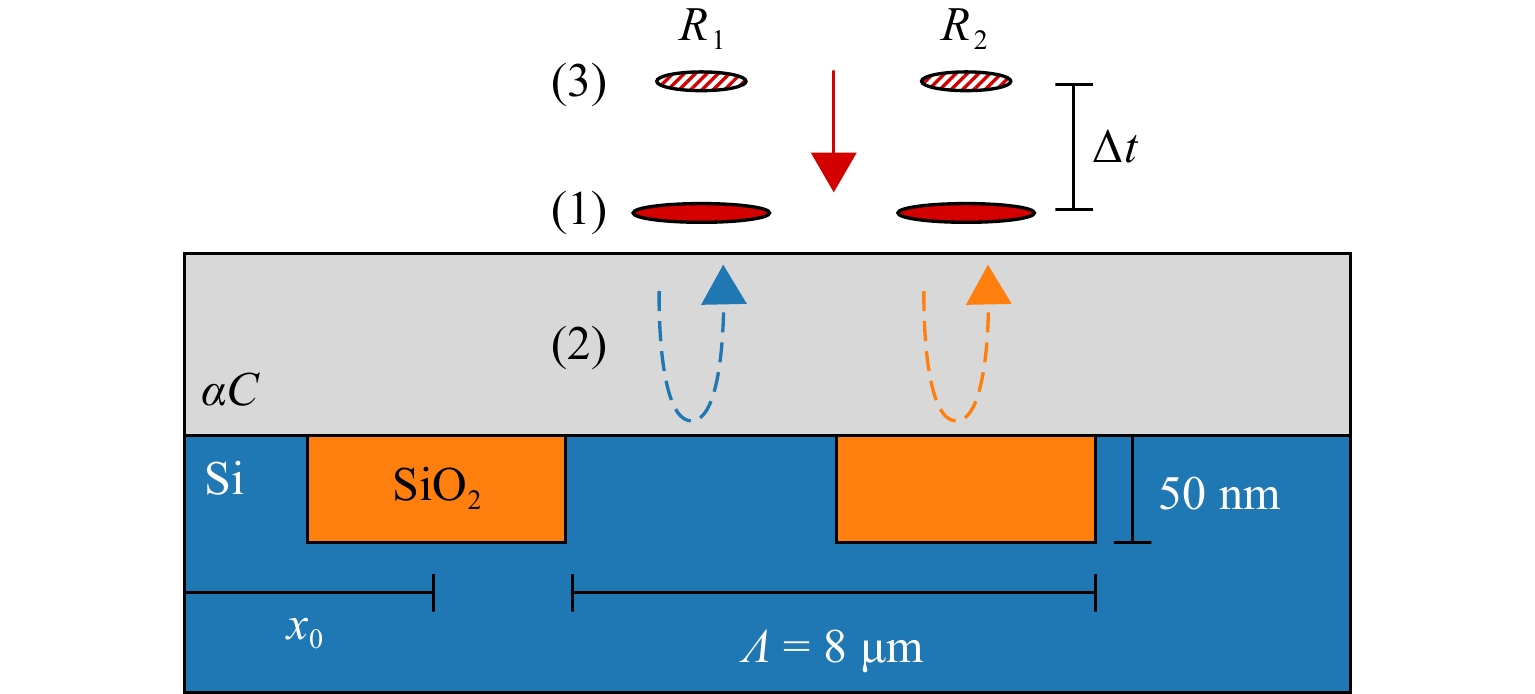
Manufacturing integrated circuits (ICs) using photolithography is the key technology enabling modern electronic devices. As advanced ICs are fabricated in multiple lithography steps, accurate metrology is crucial. For wafer alignment, optical methods are essential as they enable fast and non-invasive measurements. However, the use of optically opaque materials complicates optical metrology on markers in deeper layers. Here we present an optical metrology approach capable of nanometer-level alignment metrology through optically opaque layers. We use ultrashort laser pulses to generate high-frequency ultrasound at picosecond timescales, with which buried metrology markers can be probed. By detecting the ultrasound reflections with a second, time-delayed laser pulse, position information is obtained in an all-optical way. We demonstrate our approach on an alignment grating covered by a 1.3 μm thick layer of amorphous carbon, achieving 15 nm positioning reproducibility in 1 s measurement time, with significant potential for further scaling. This measurement concept will help advance semiconductor manufacturing, by enabling optical wafer metrology on future devices featuring layers of metals and other opaque materials.


Published
, Published online: 18 June 2026
, doi: 10.37188/lam.2026.080
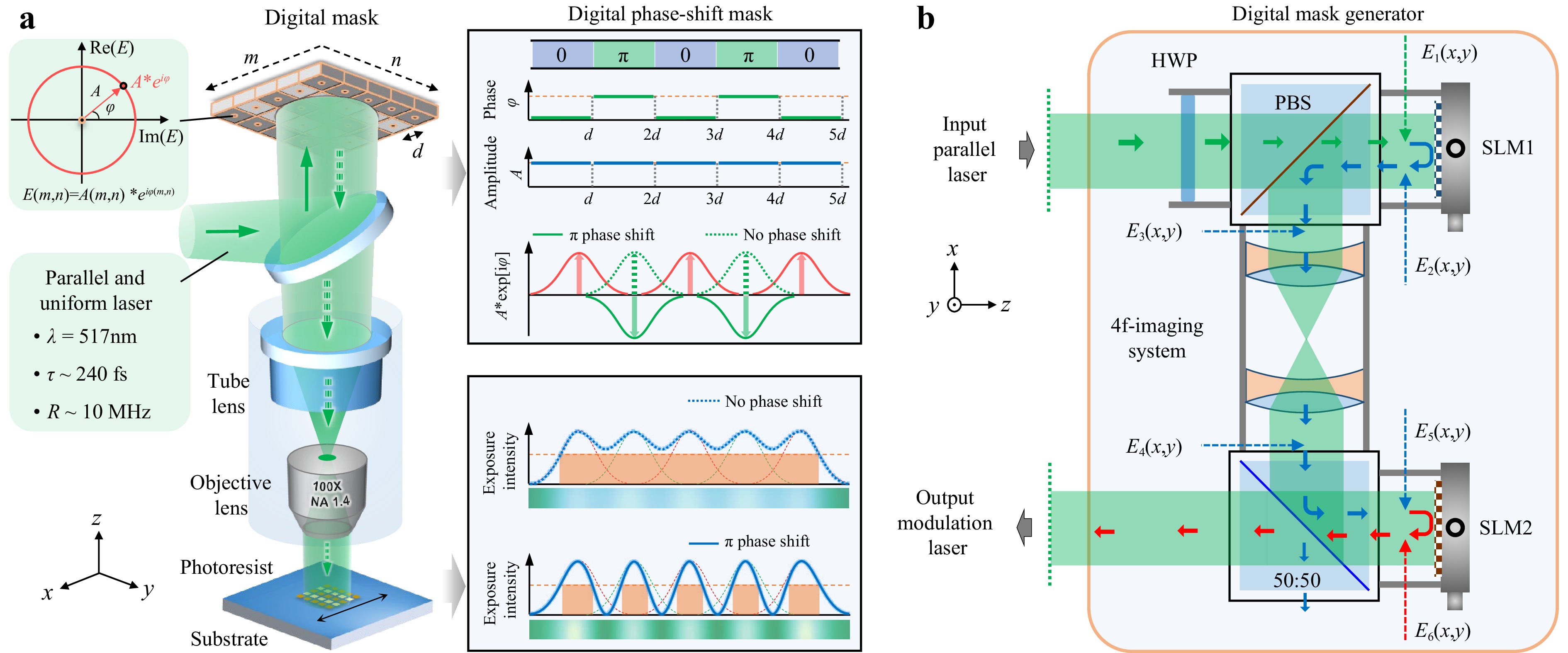
The diffraction limit poses a fundamental challenge to digital mask projection lithography (DMPL) in fabricating subwavelength-scale dense periodic patterns, limiting its application in advanced chip manufacturing. To address this, we present a DMPL platform with a resolution-enhancement strategy combining a digital phase-shifting mask with two-photon polymerisation. The method enables precise control of subwavelength structure distribution while preserving DMPL flexibility. Using alternating phase-shifting modulation through cascaded spatial light modulators under 517 nm femtosecond laser illumination, we achieve near-physical-limit resolution in a single exposure, producing line patterns with a critical linewidth of ~60 nm (0.16 λ/NA) and a single-exposure pitch resolution of ~235 nm (half pitch ~0.32 λ/NA). With a double-exposure strategy, the pitch is further reduced to ~158 nm (half pitch ~0.21 λ/NA), enabling robust sub-diffraction-limit patterning. This approach advances diffraction-limited patterning and offers new possibilities for manufacturing nanophotonic devices and next-generation microelectronic components.


Published
, Published online: 09 June 2026
, doi: 10.37188/lam.2026.076
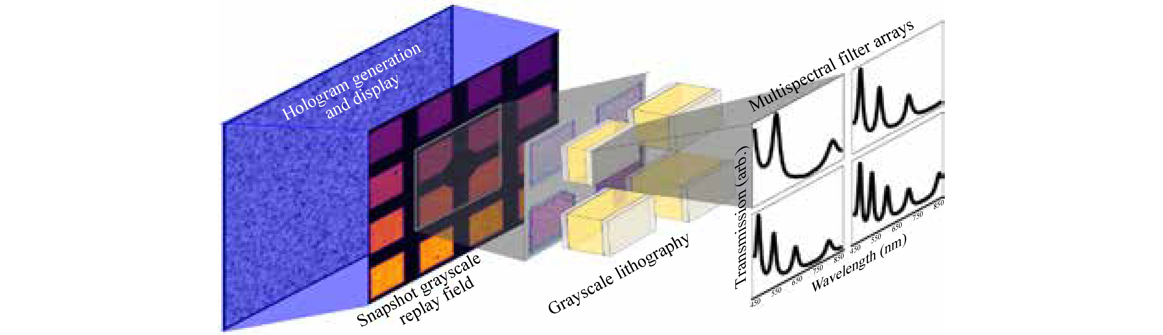
Multispectral filter arrays underpin compact spectral imaging but are typically fabricated through complex multistep photolithography. Herein, we demonstrate a single-step holographic grayscale lithography method that uses a spatial light modulator to directly write Fabry-Perot filter arrays. A phase-retrieval algorithm is used to compute holograms that project grayscale intensity patterns onto a photoresist, enabling cavity thicknesses ranging from 600 to 1,300 nm across a single exposure. In this study, transmission spectra were modelled using transfer-matrix simulations with Monte Carlo averaging to capture thickness variations, and experimental spectra were fitted via Tikhonov-regularized inversion. Good agreement was observed between the theory and experiment (R2 \begin{document}$\approx$\end{document}


Published
, Published online: 05 June 2026
, doi: 10.37188/lam.2026.020
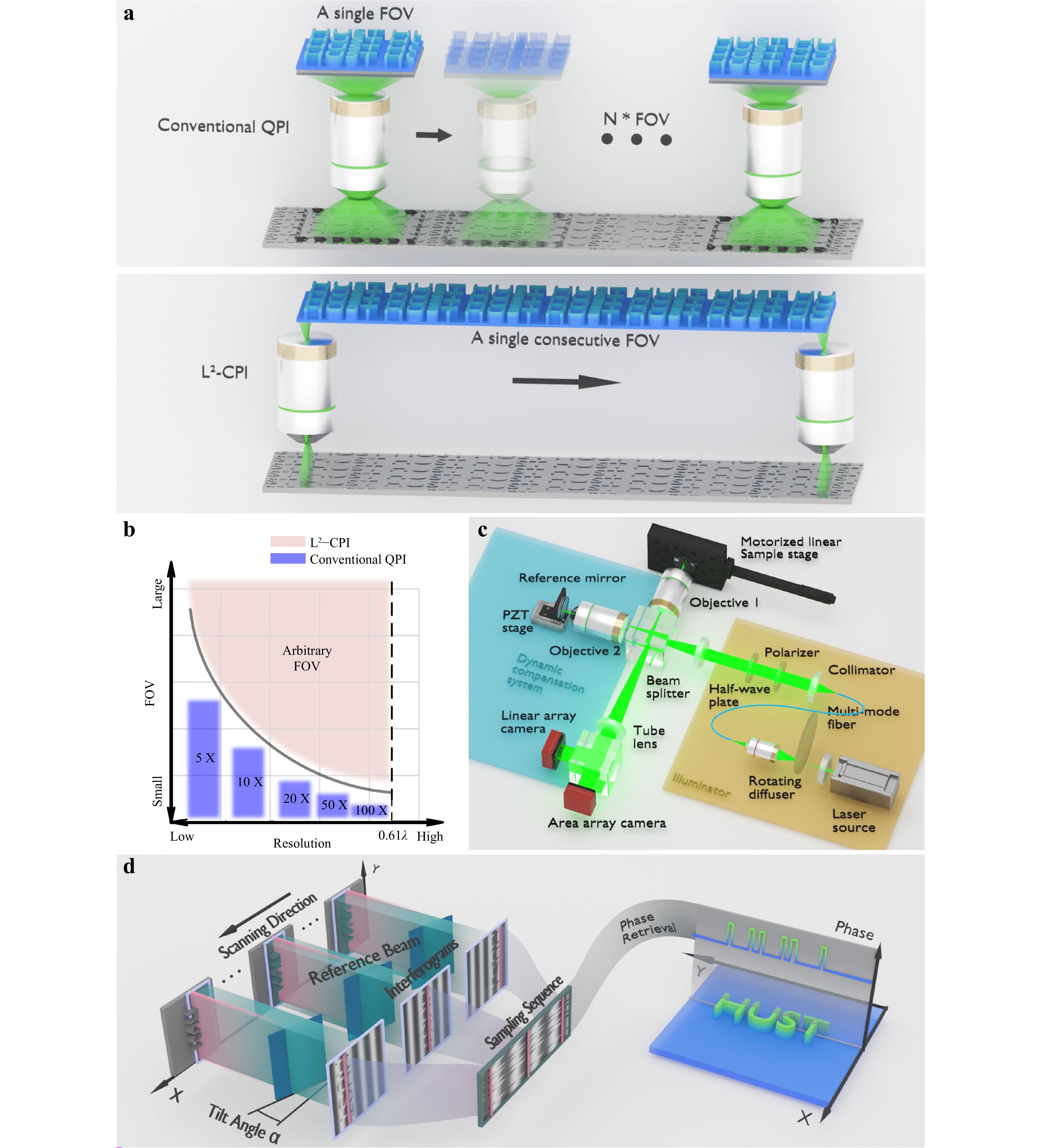
Optical phase imaging is a powerful tool widely used in bioimaging, material characterization, pathology, and nanomanufacturing. Yet, it faces a persistent challenge: the inherent contradiction between resolution and field of view (FOV) in conventional microscope-based systems. To address this limitation, we propose Lateral Line-Scan Computational Phase Imaging (L2-CPI), a novel computational phase imaging architecture that enables consecutive phase imaging of moving samples. Our experiments with both transparent and opaque samples demonstrate that L2-CPI achieves an equivalent FOV of D × L, where D is the camera sensor edge length and L is the motorized stage travel range. This implies that the equivalent FOV of L2-CPI in a single measurement can be arbitrarily large, provided the stage travel range L is arbitrarily long. Our work breaks the long-term contradiction between resolution and FOV, establishing a new paradigm for ultra-large-FOV phase imaging in dynamic mode without sacrificing optical resolution. This advancement holds significant potential for applications in bioimaging, material characterization, biosensing, nanometrology, and semiconductor inspection.


Published
, Published online: 03 June 2026
, doi: 10.37188/lam.2026.034
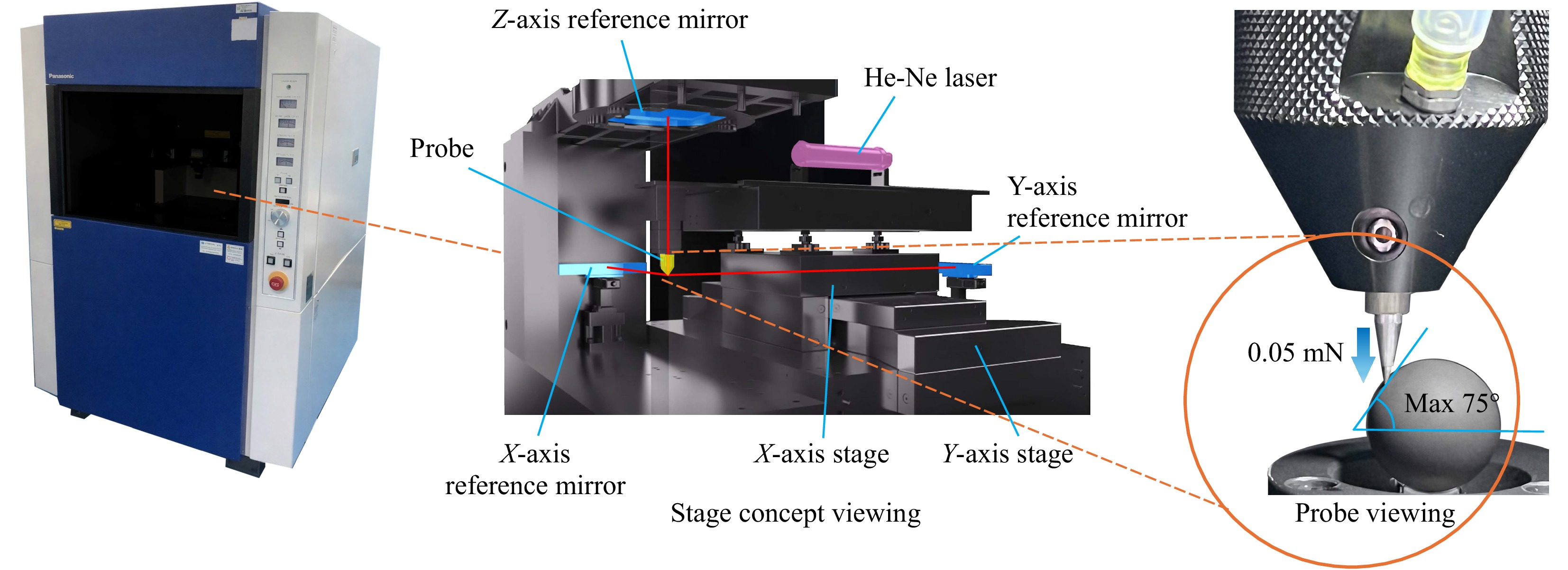
With the rapid growth of extended-reality (XR) devices, simultaneously achieving long optical path length and miniaturization has become a central challenge in optical system design. One promising approach is to employ optical designs that utilize multiple internal reflections in a prism to extend the path length within a compact volume. The prisms targeted in this study are polyhedral elements composed of three or more optical surfaces including freeform surfaces, in which two lateral faces are mutually parallel. A representative example is a triangular prism whose optical faces are replaced by freeform surfaces. Because such prisms contain multiple reflecting faces, their inter-surface positional relationships must be formed and maintained with high accuracy; consequently, metrology capable of precise evaluation of face-to-face position is indispensable for production. Since 2002, Panasonic has introduced to the market inter-surface misalignment evaluation of lens surfaces using the ultra-high-accuracy three-dimensional profilometer UA3P, contributing to higher-precision camera modules. Building on that platform, the present work develops a new measurement method that extends the UA3P system to prisms with multiple reflecting faces, enabling spatial registration to be evaluated with an accuracy of 0.2–0.3 µm. The developed system shows strong correlation with existing methods and validated repeatability, demonstrating its suitability for high-precision manufacturing and quality assurance of optical elements, including prisms for XR devices.


Published
, Published online: 26 May 2026
, doi: 10.37188/lam.2026.063
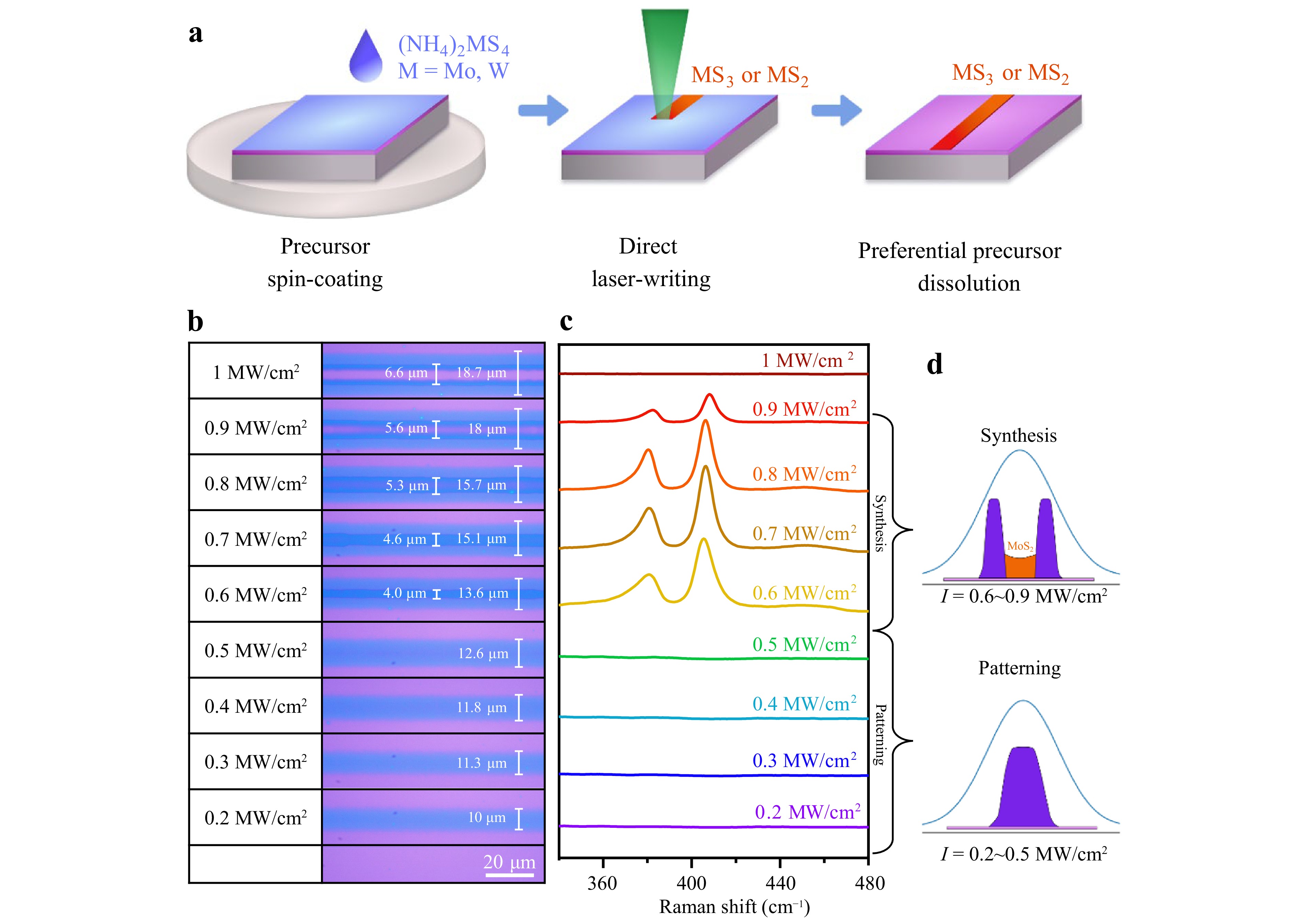
Transition metal dichalcogenides (TMDCs) are promising layered materials for nanophotonics because of their inherent optical anisotropy, large refractive indices, and optical non-linearity, which make them excellent candidates for integration into photonic components. However, current prototyping techniques used to fabricate functional photonic elements rely on post-processing of single-crystal flakes or chemical vapour deposition (CVD)-grown films via focused ion beam milling, which is a throughput-limited and time-consuming approach. Therefore, scalable and rapid patterning methods for TMDC-based photonic devices are required to boost their application in the field of photonic technologies. Herein, we present a laser lithography method that enables the direct production of ultrafine diffractive MoS2 and WS2 structures from their chemical precursors. Thin films of thiosalt precursors, spin-coated onto various substrates, can be patterned with high resolution when exposed to light in the visible and ultraviolet (UV) spectral regions in a photolithographic manner. This allows either the direct synthesis of TMDC structures or the production of micro/nanopatterns consisting of partially synthesised amorphous material from the initial precursor films, which can later be converted to the desired TMDC using a two-step process. Using interferometric lithography, we fabricated of MoS2 and WS2 diffraction gratings with periods as short as 150 nm and aspect ratios ~104 (length/width), as well as MoS2 Fresnel holograms on photonic substrates such as silica (SiO2) and lithium niobate (LiNbO3). An MoS2 grating coupler was fabricated and used to couple light onto a thin-film lithium niobate planar waveguide. The measured diffraction efficiencies of the laser-patterned multi-layer MoS2 gratings at visible wavelengths matched the corresponding values reported for exfoliated TMDC materials, highlighting the potential of this method for fabrication of 2D photonics.


 Email
Email RSS
RSS