
2026 Vol. 7, No. 1
Published. 2026, 7(1)
: 5-7
doi: 10.37188/lam.2026.015
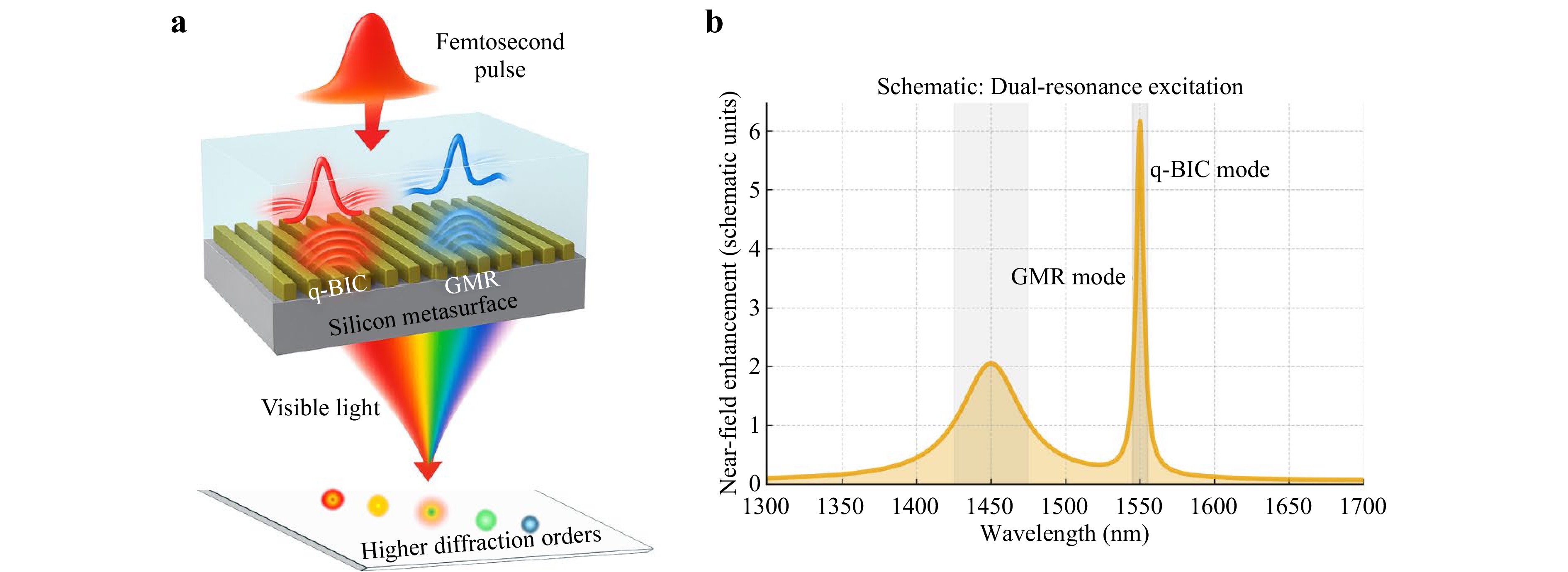
Nonlinear metasurfaces are transforming wavefront control at the nanoscale, offering compact platforms for efficient frequency conversion and all-optical processing. In a recent advance, Franceschini et al. demonstrated a powerful method to generate tunable visible light by exploiting nonlinear coupling between two distinct resonances in an amorphous-silicon metasurface, all driven by a single broadband femtosecond pulse.
Published. 2026, 7(1)
: 8-10
doi: 10.37188/lam.2026.023
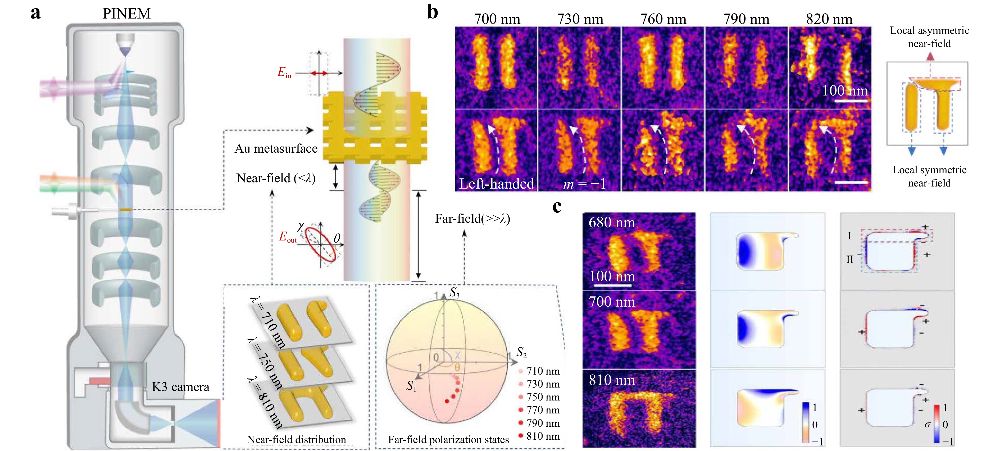
In chiral metasurfaces, experiments reveal that circular dichroism (CD) is fundamentally dictated by asymmetric near-fields that are locally generated within individual meta-atoms. This work quantitatively establishes a sequential causal chain in which the geometric asymmetry of a meta-atom drives the selective excitation of specific eigenmodes and the emergence of chiral near-fields, which are manifested as the far-field CD response. Through this clarified linkage between geometry, modal responses, and optical chirality, chiral metasurface design can advance toward geometry-driven mode at the meta-atom level.
Published. 2026, 7(1)
: 11-13
doi: 10.37188/lam.2026.019
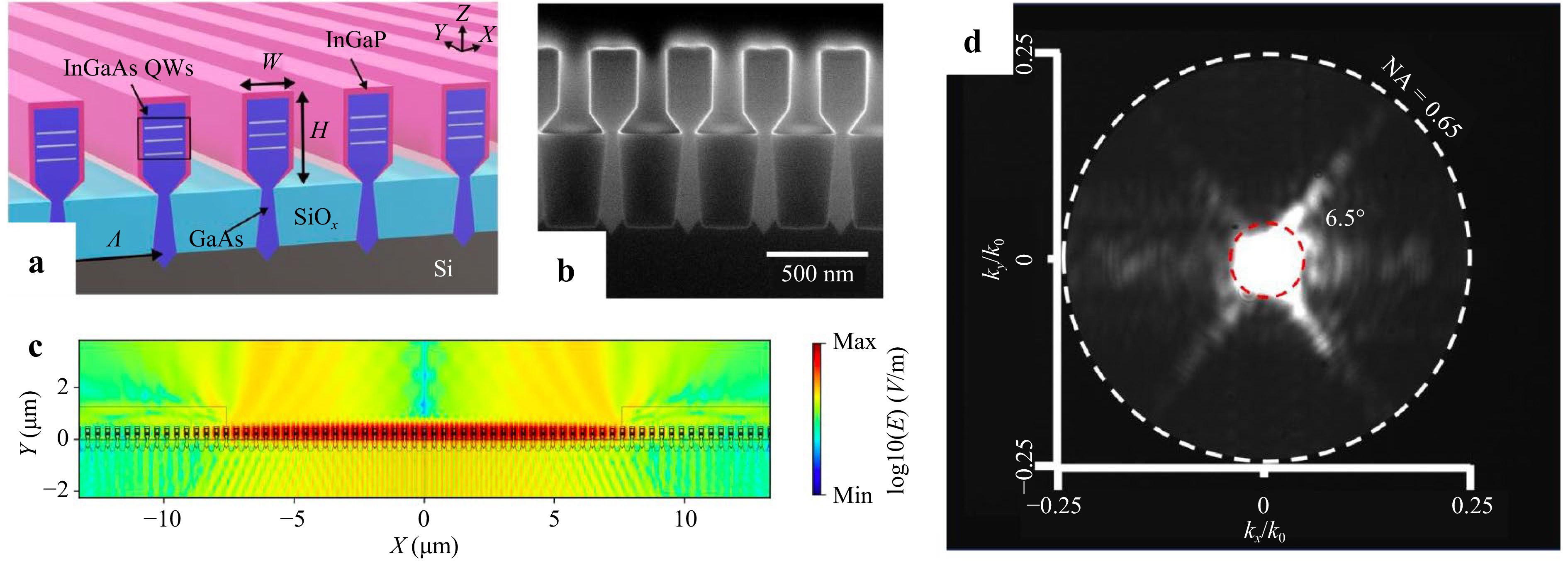
Directly growing III-V lasers on 300 mm silicon wafers is a crucial step for future photonic integrated circuits. While recent work has achieved electrically-pumped in-plane lasing, new research has shown that surface emission can be efficiency achieved by modifying the heteroepitaxy of InGaAs/GaAs nano-ridges to form a one-dimensional photonic crystal, opening a new direction for scale-up of high-density surface emitting lasers on silicon.
Published. 2026, 7(1)
: 14-16
doi: 10.37188/lam.2026.018
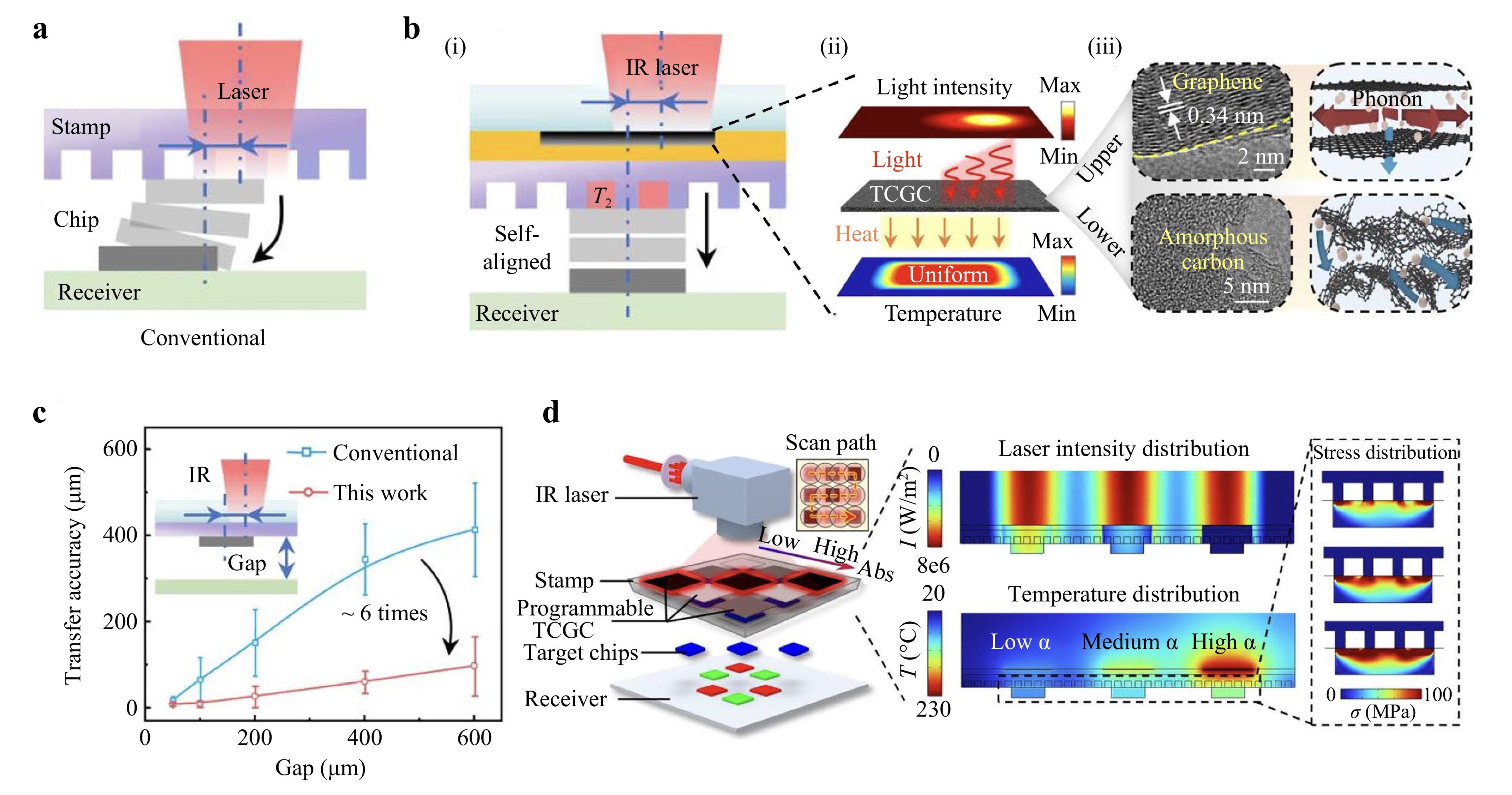
Gradient-graphene-enabled directional photothermal regulation is proposed and demonstrated to achieve uniform heat distribution in the laser-sensitive layer, thereby enhancing the accuracy of self-aligned laser transfer printing.
Published. 2026, 7(1)
: 17-18
doi: 10.37188/lam.2026.017
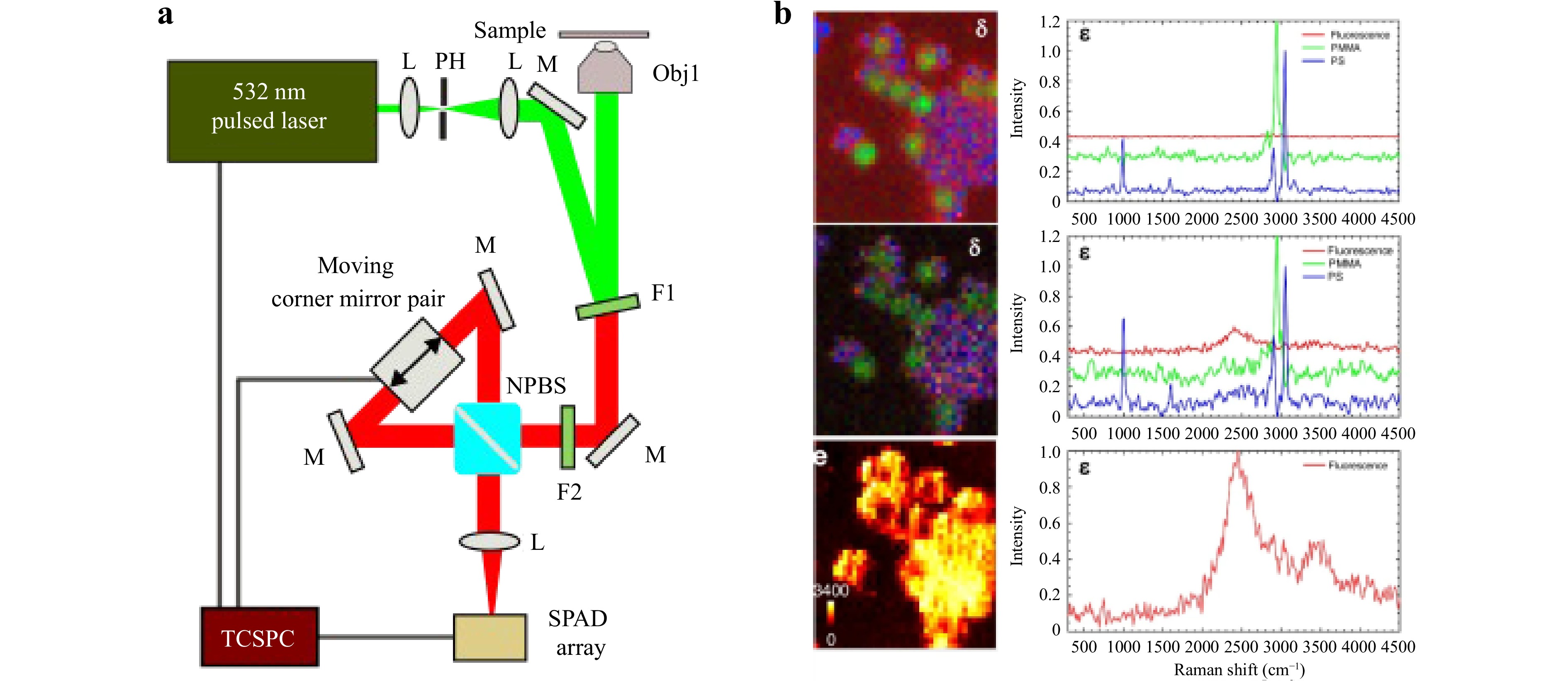
Fourier-transform time-gated Raman imaging is proposed and demonstrated. By developing a detection arm utilizing a SPAD array and a high performing interferometer, the system can achieve both high temporal and spectral resolution and strong separation between Raman and fluorescence signals.
Published. 2026, 7(1)
: 19-20
doi: 10.37188/lam.2026.016
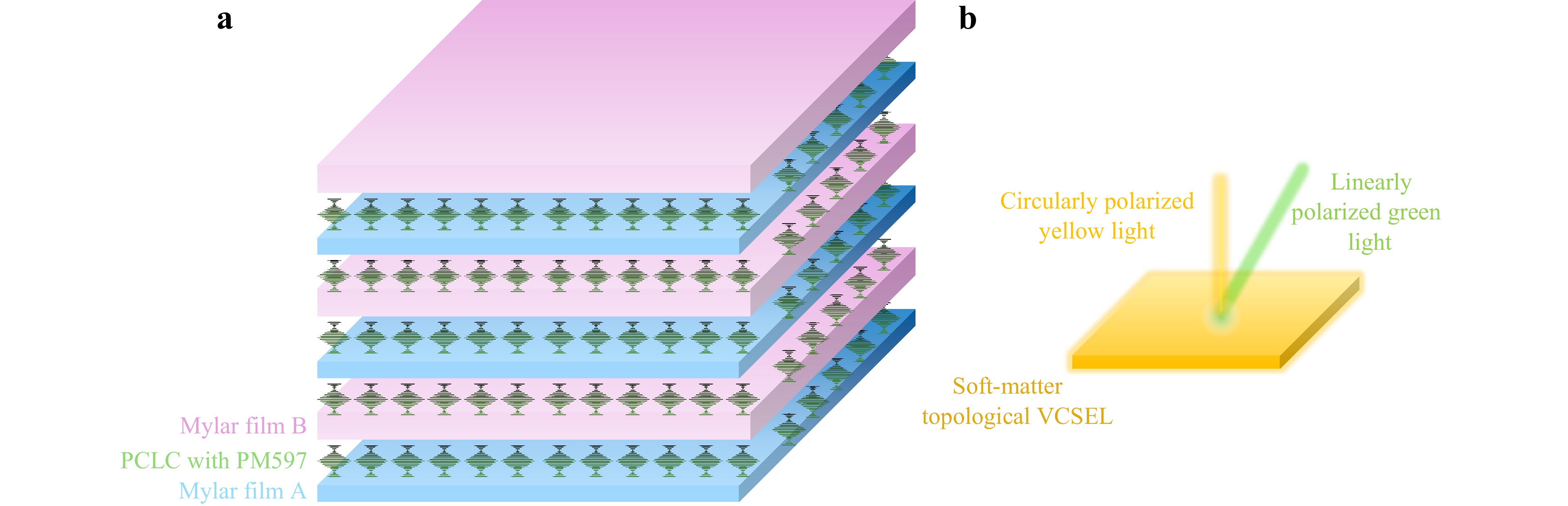
A new soft-matter vertical-cavity surface-emitting laser (VCSEL) based on stacked Mylar films and polymerized cholesteric liquid crystal films holds great potential for fabricating flexible lasers, which is sought after in many emerging applications.
Published. 2026, 7(1)
: 21-24
doi: 10.37188/lam.2026.014
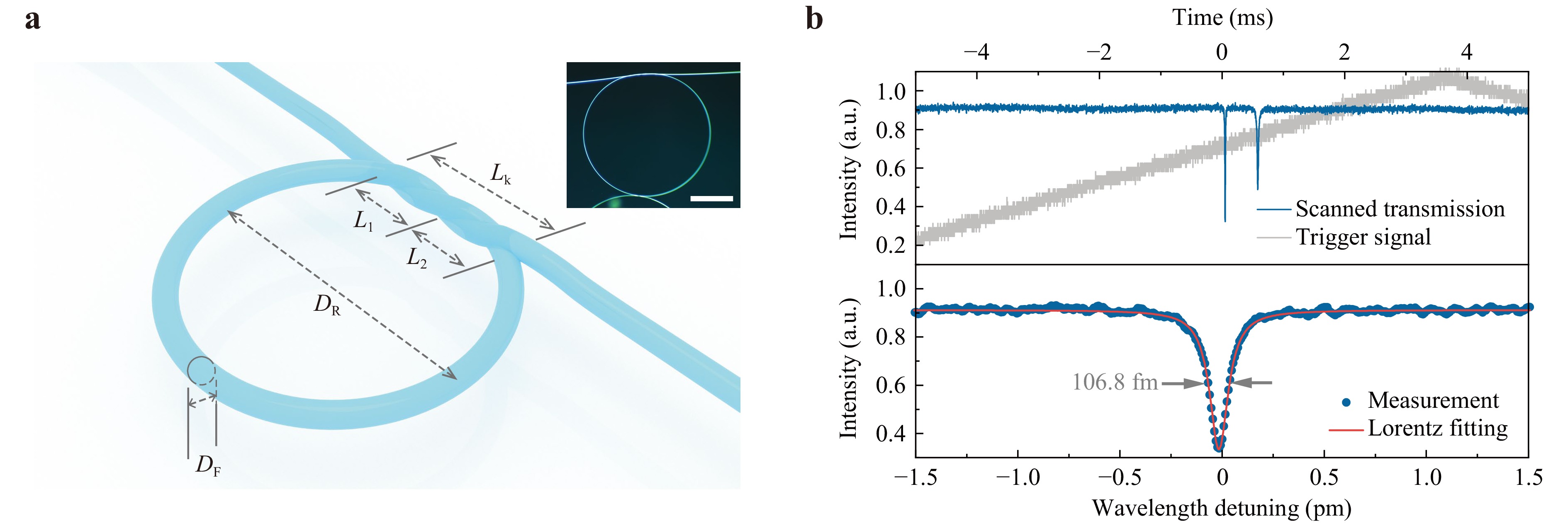
Zhou et al. achieved a record-breaking quality factor (Q-factor) of 3.9×10⁷ in microfibre knot resonators (MKRs) through optimised environmental control and coupling tuning, enabling stable single-frequency lasing and establishing a foundation for advanced photonic applications.
Published. 2026, 7(1)
: 25-27
doi: 10.37188/lam.2026.012
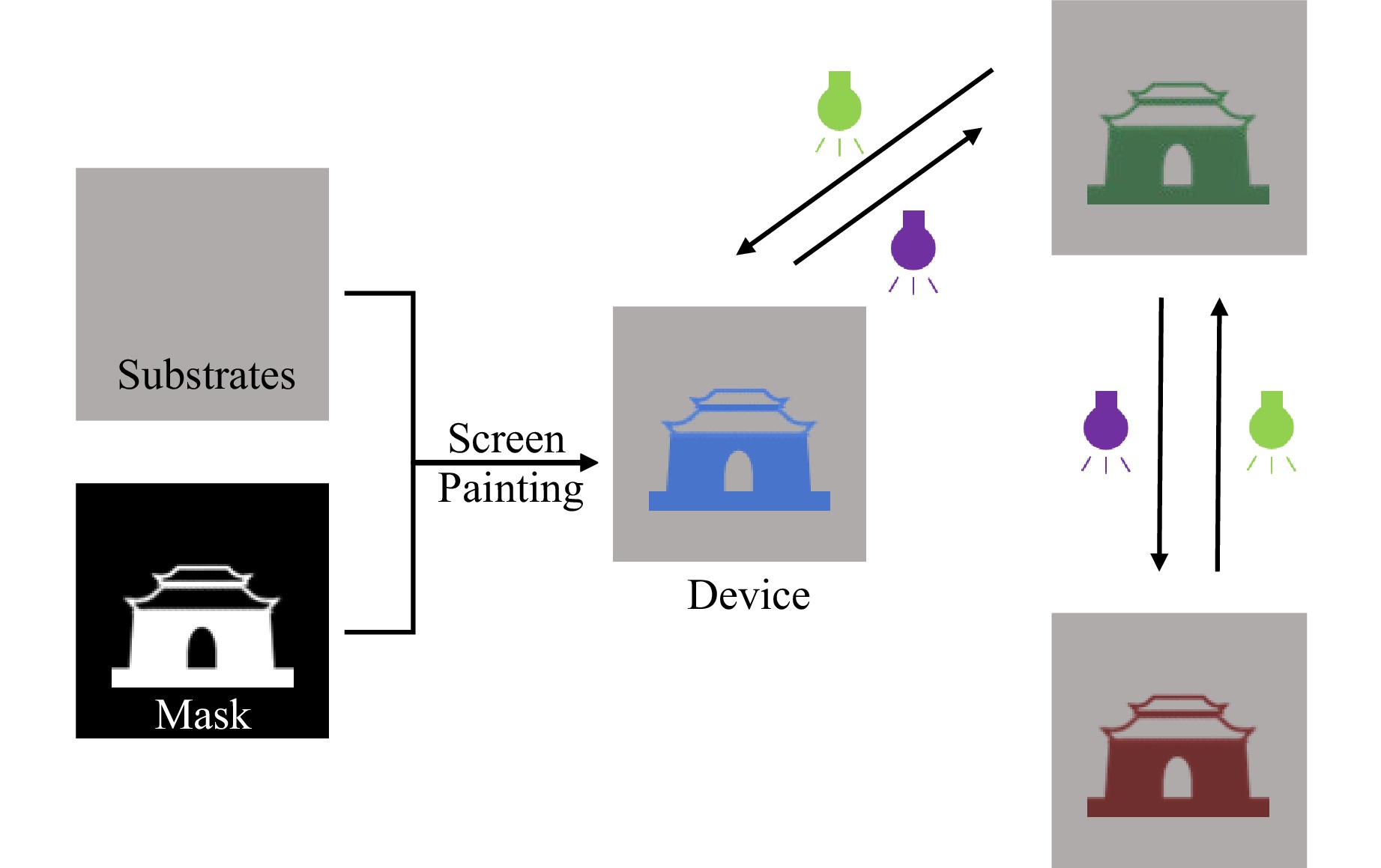
Patterned photonic crystals that exhibit structural colours attract considerable attention owing to their exceptional color saturation and variability. A unique paintable helical photonic architecture featuring both multi-stability and dynamic light-actuation is proposed. The method shows great potential for applications in anti-counterfeiting, information encryption, and smart windows.

Published. 2026, 7(1)
: 28-30
doi: 10.37188/lam.2026.011
A polarization-sensitive neuromorphic vision sensor based on black arsenic-phosphorus, an anisotropic 2D material, can seamlessly integrate perception, memory, and computation. This device features flexible synaptic plasticity, enabling a hybrid neural network to achieve high accuracy in image tasks and demonstrating high-fidelity polarization-resolved imaging. This is a significant step toward compact and brain-inspired optoelectronic systems.

Published. 2026, 7(1)
: 31-32
doi: 10.37188/lam.2026.010
Multidimensional light-field control is opening new frontiers in photonics. Recent breakthroughs in metasurface design and the integration of Dammann optimisation with spin-decoupled phase modulation enable the simultaneous manipulation of phase, amplitude, polarisation, and orbital angular momentum to project information into three-dimensional space. This paradigm shift towards full-parameter control in stereoscopic volumes is promising for revolutionising applications from high-capacity optical communications to secure encryption and parallel computing, marking a significant advancement in integrated photonic systems.
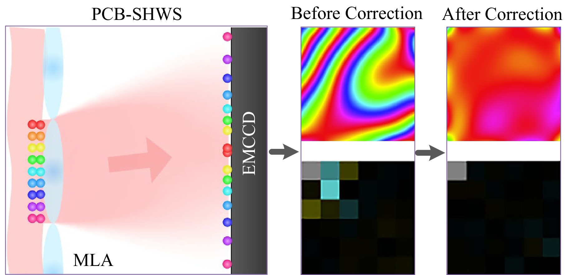
Published. 2026, 6(1)
: 33-34
doi: 10.37188/lam.2026.005
Position-correlated biphoton Shack-Hartmann wavefront sensing is proposed and experimentally demonstrated. Based on this approach, the biphoton correlation propagating through phase turbulence can be measured and corrected, thus enabling adaptive quantum imaging against phase disturbances with only a single-shot measurement.
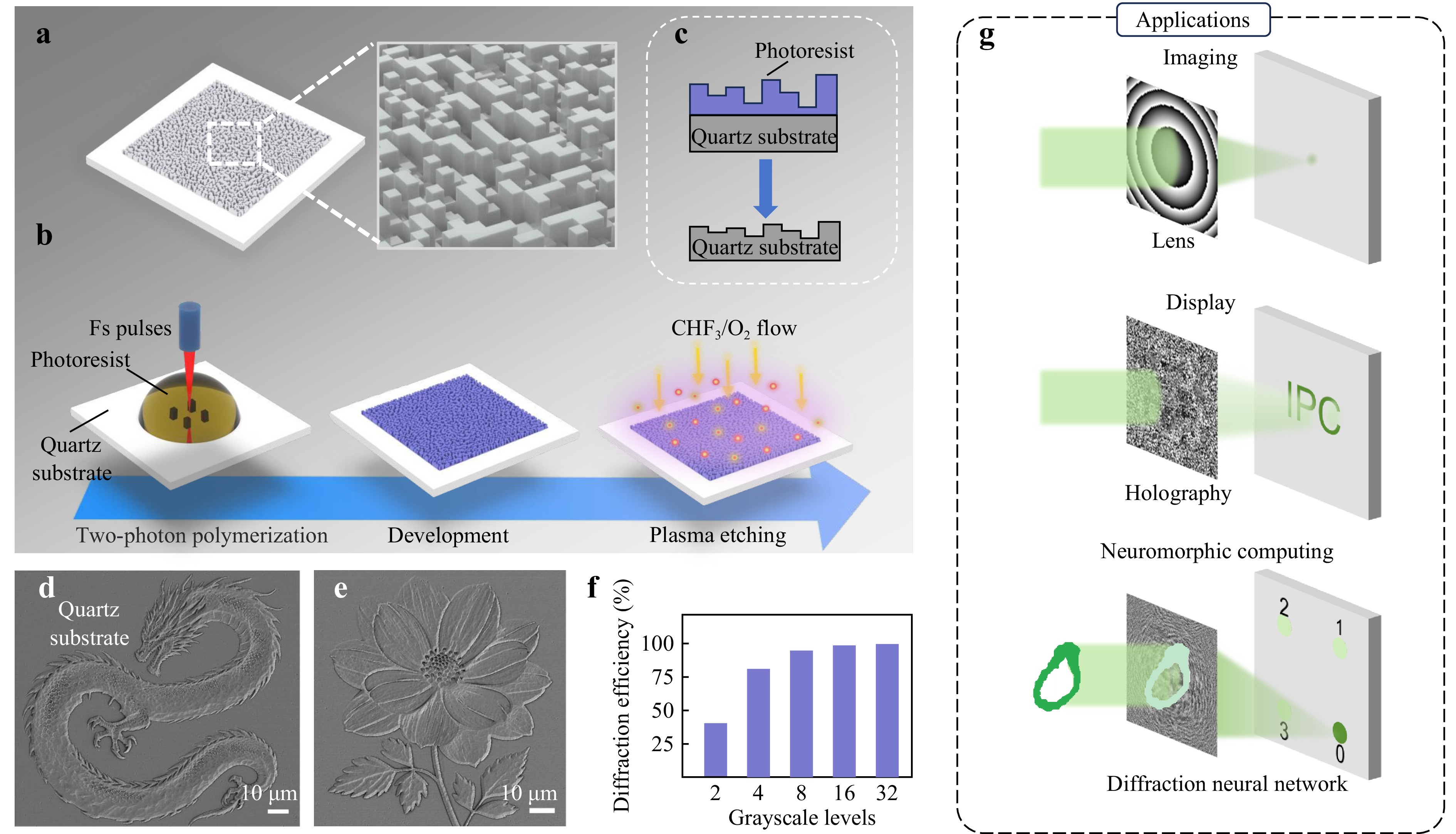
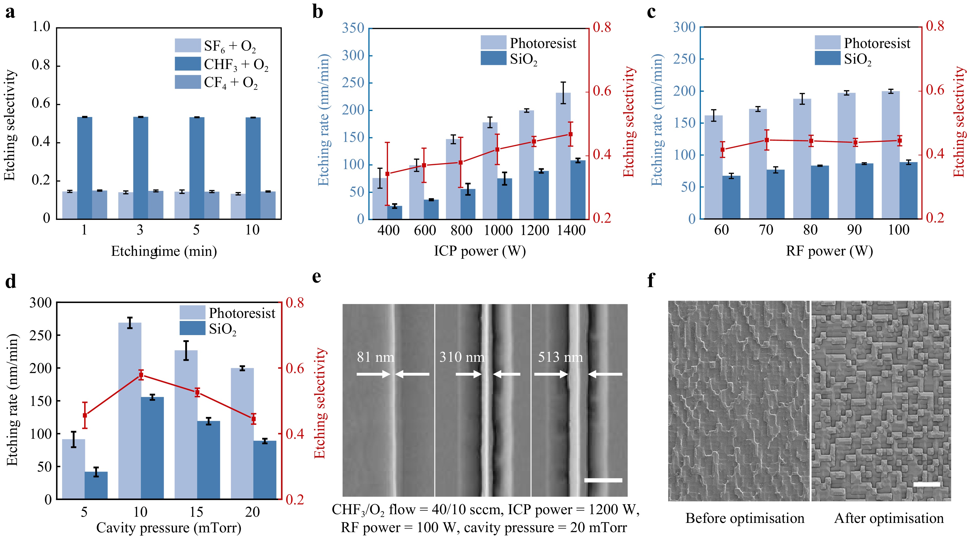
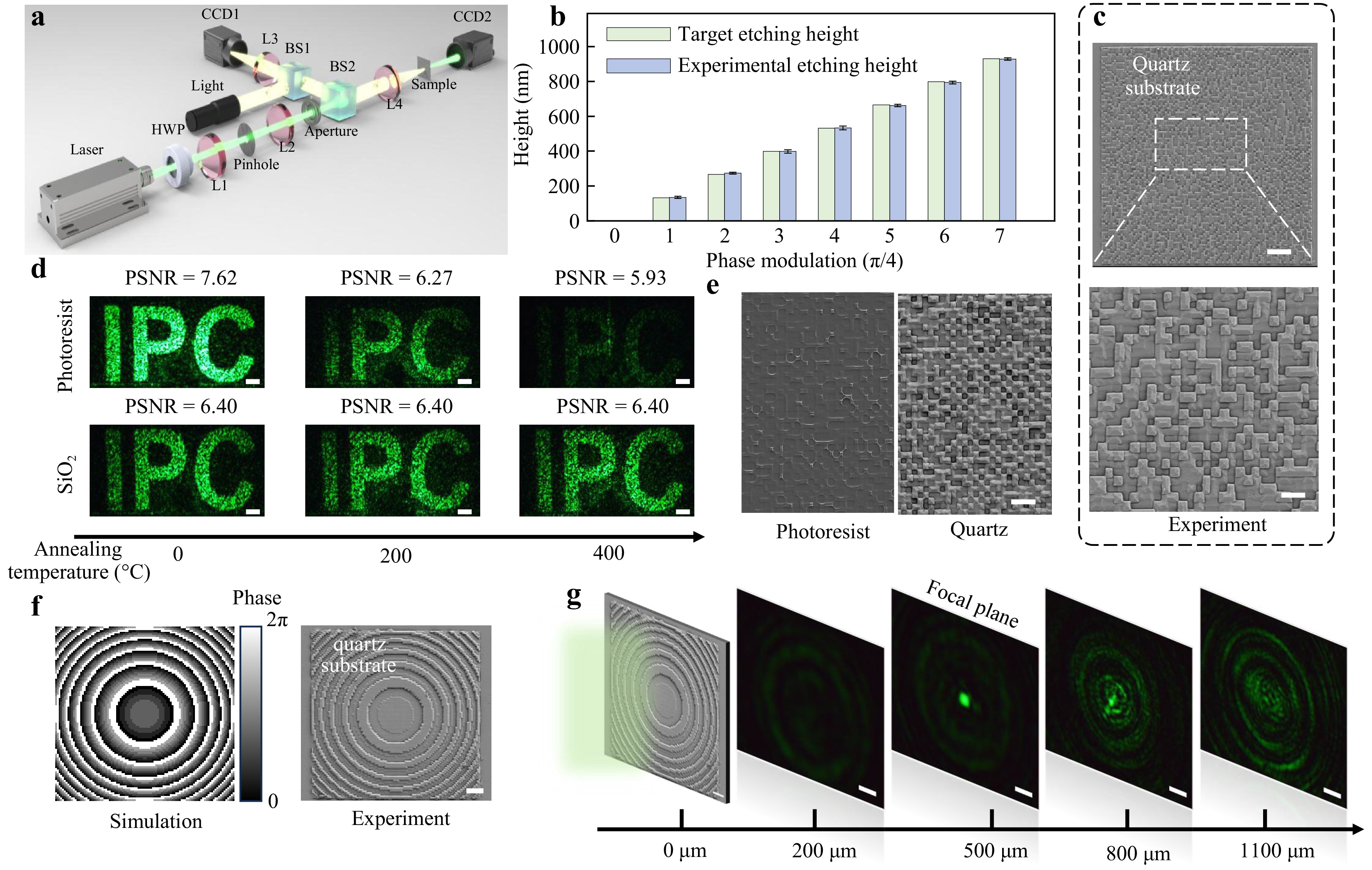
Published. 2026, 7(1)
: 35-44
doi: 10.37188/lam.2026.031
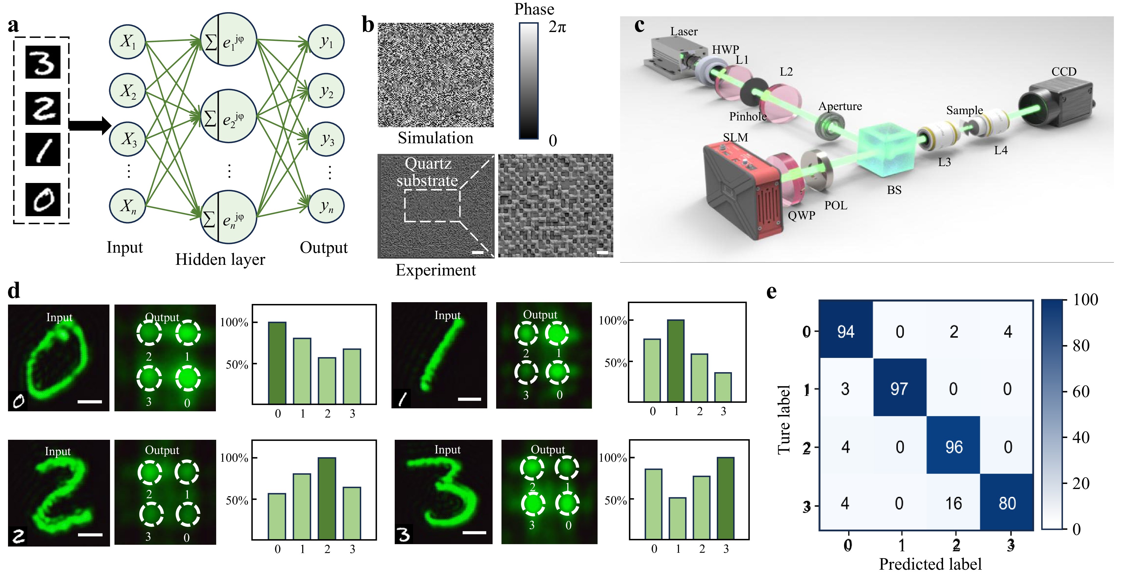
To overcome the resolution and stability limitations of conventional grayscale lithography, we present a laser-nanoprinting-assisted technique for multilevel nanoscale phase encoding on a quartz substrate. The proposed approach combines femtosecond laser-based grayscale mask fabrication with multiparameter dry etching optimisation to achieve precise phase modulation with subwavelength resolution approximately 81 nm) and pixel sizes as small as 1 μm2. Up to eight discrete phase levels are supported, enabling efficient diffraction control and device-level functionality. Using this method, various integrated diffractive devices, including lenses, holograms, and diffractive neural networks (DNNs), were realised on quartz substrates. The fabricated structures exhibit high pattern fidelity, mechanical and chemical robustness, and compatibility with standard photonic integration platforms. Notably, a single-layer quartz-based DNN achieved a classification accuracy of 91.75% across four classes of handwritten digits. This nanoprinting-enabled strategy provides a scalable and stable pathway for fabricating compact, multifunctional, and high-resolution diffractive photonic devices.
Published. 2026, 7(1)
: 45-59
doi: 10.37188/lam.2026.009
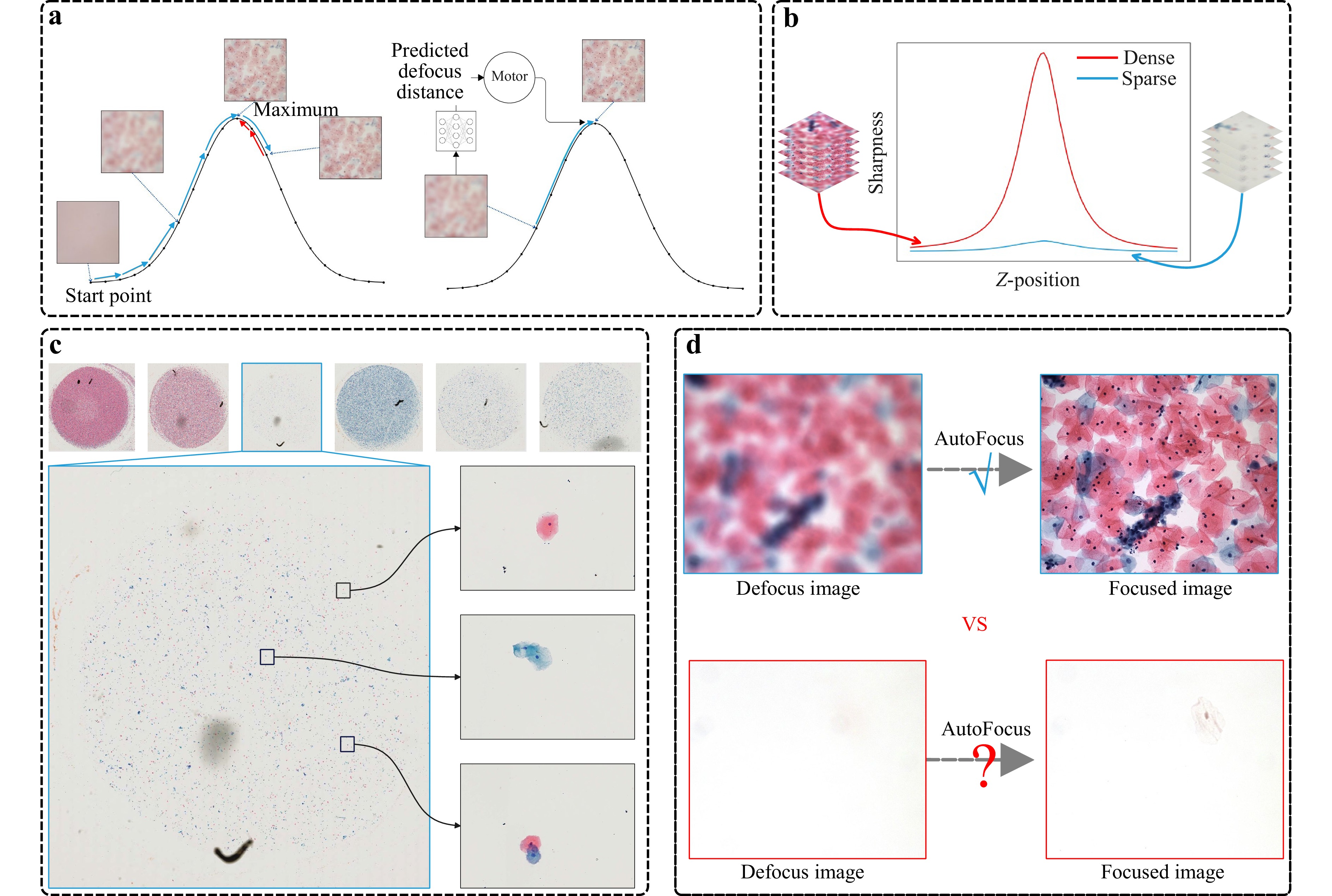
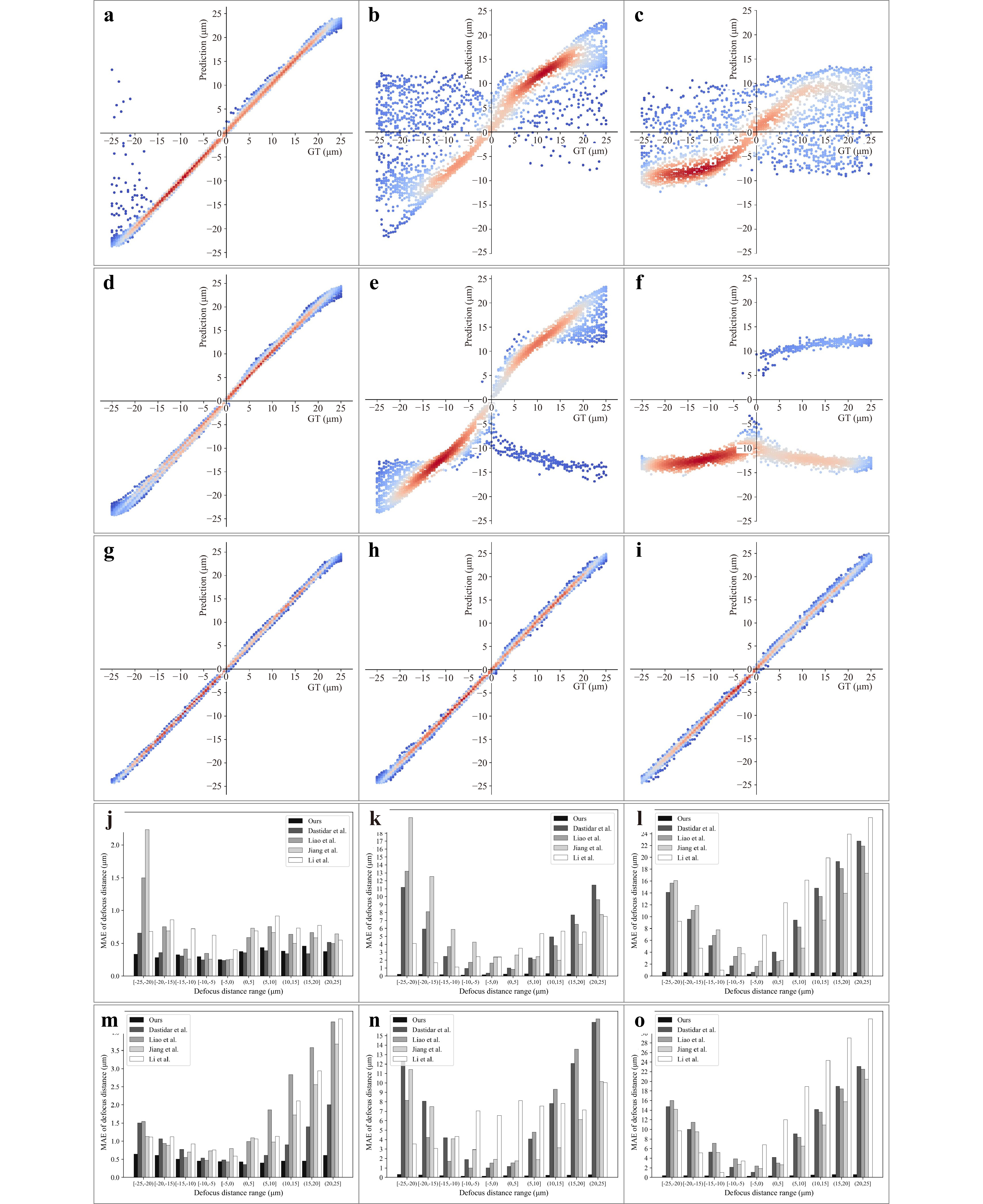
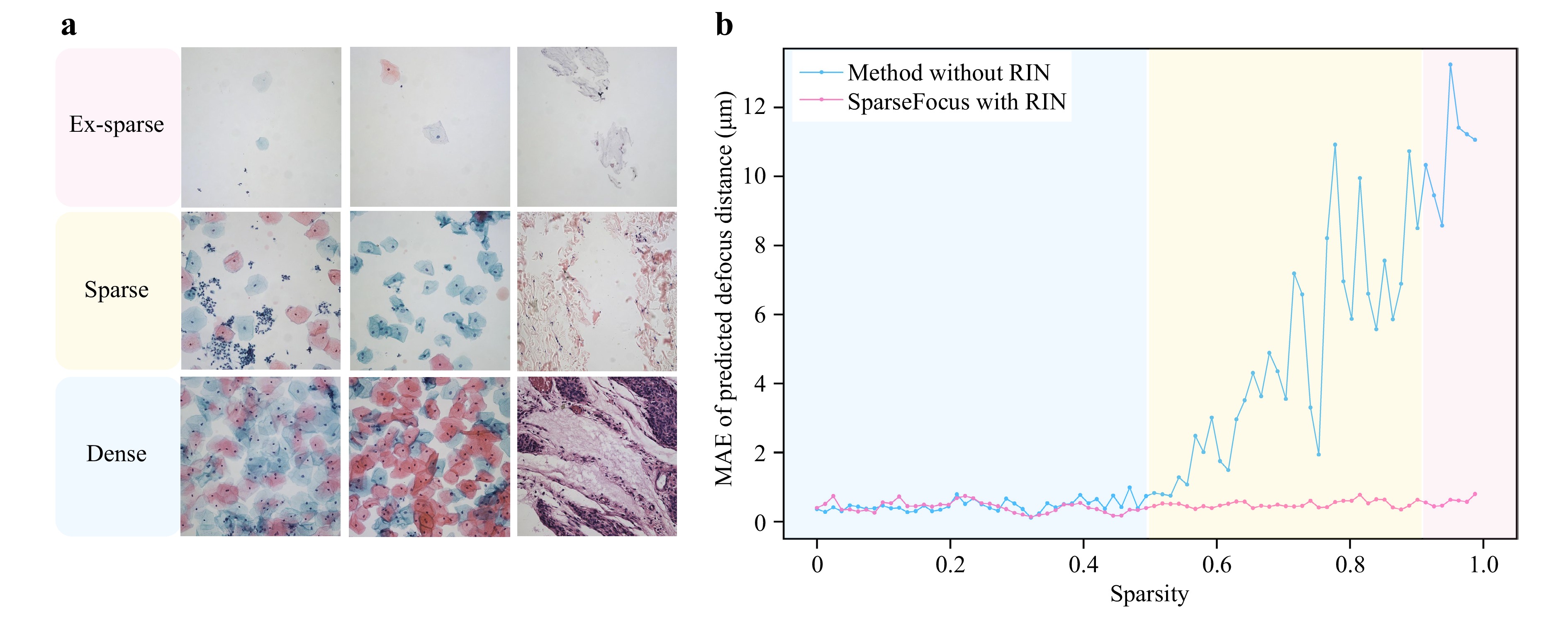
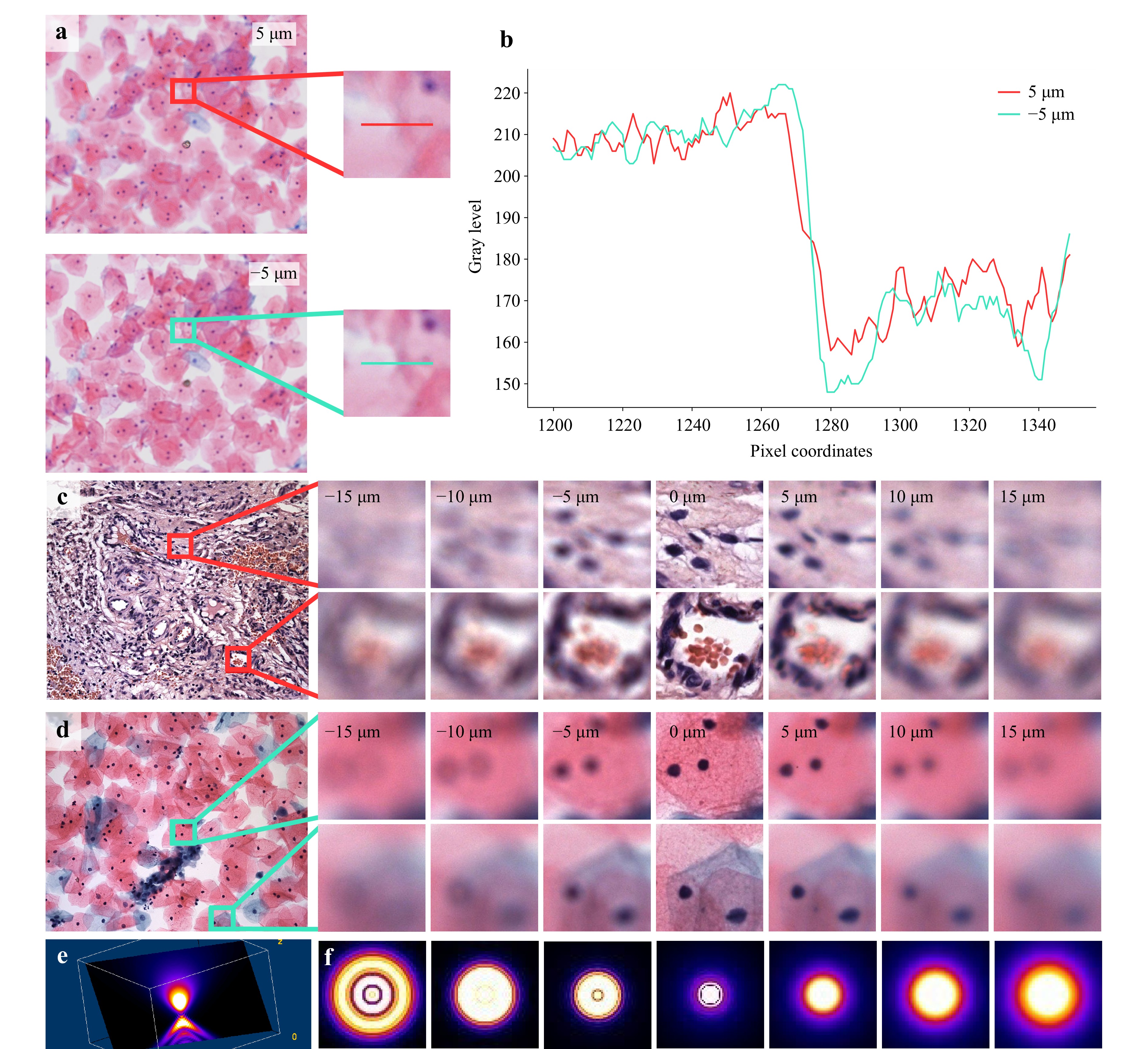
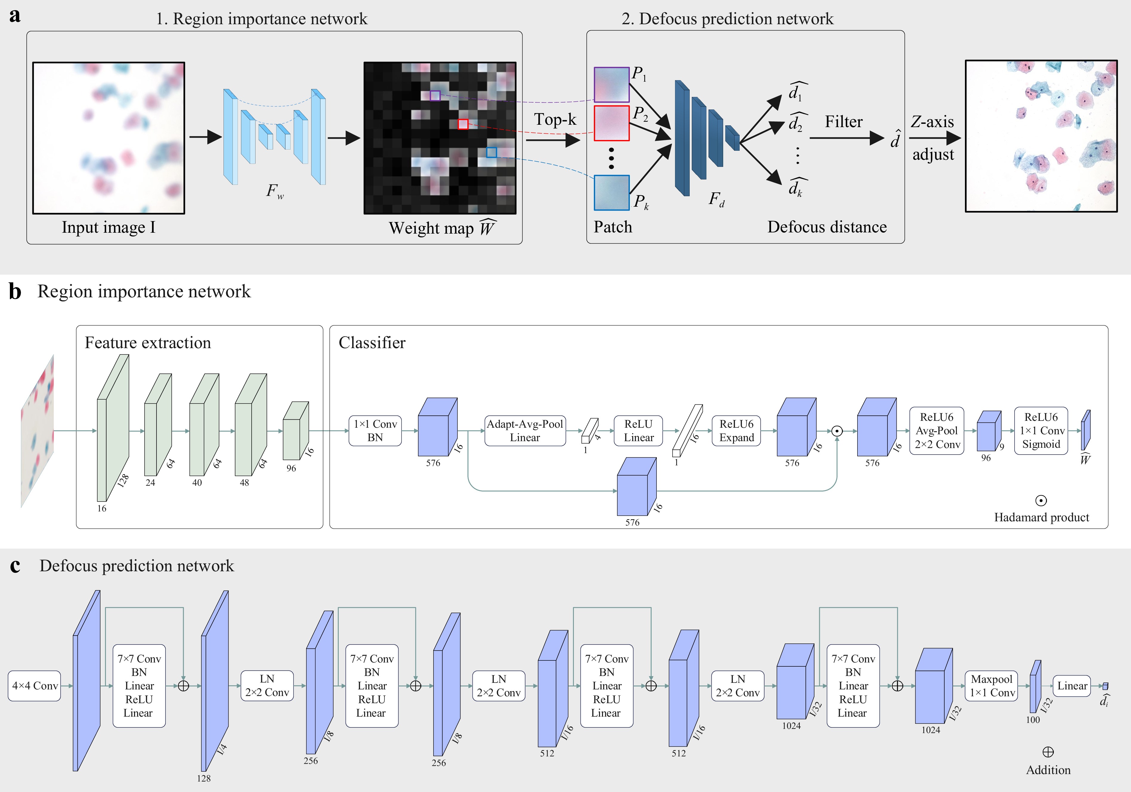
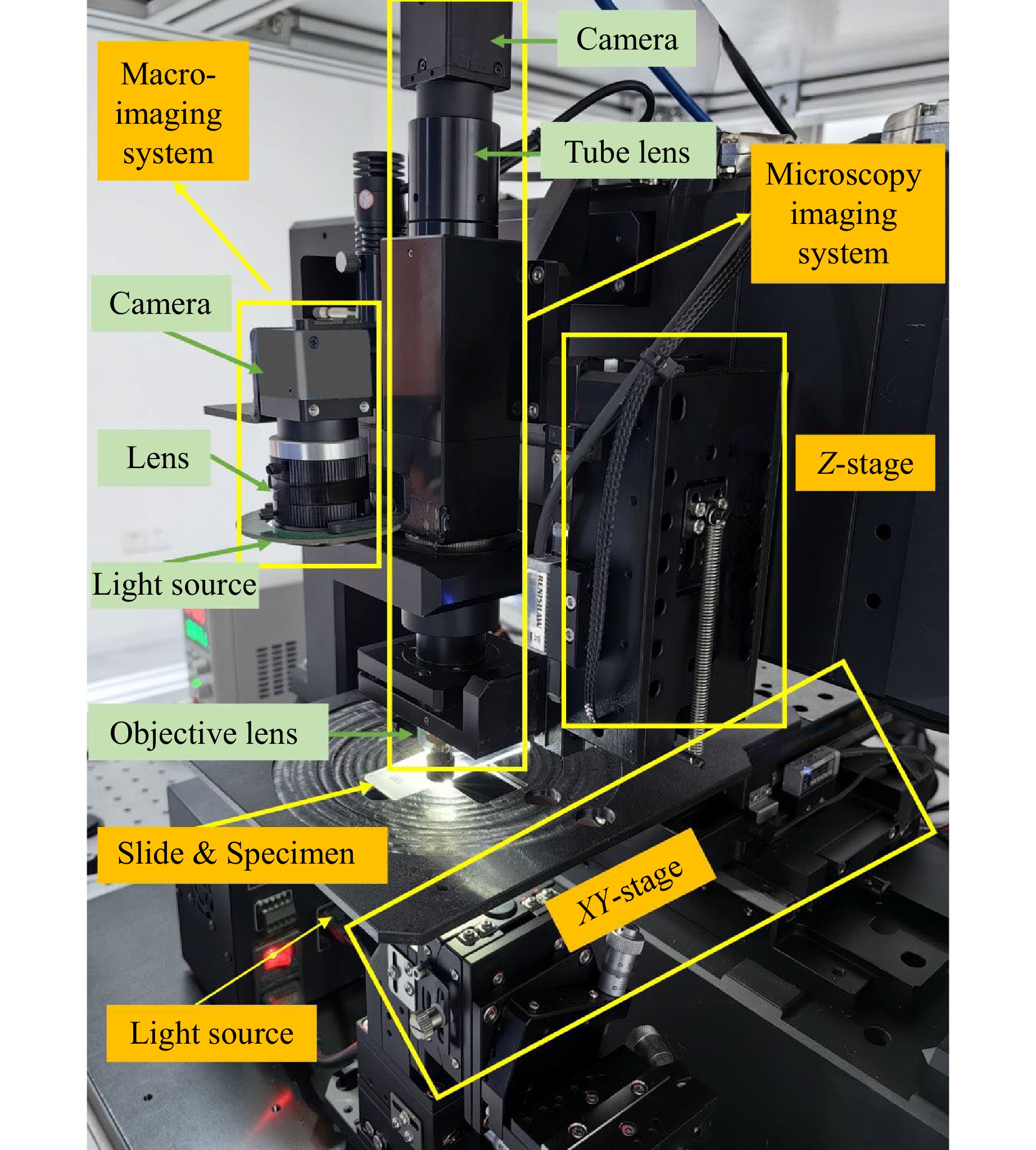
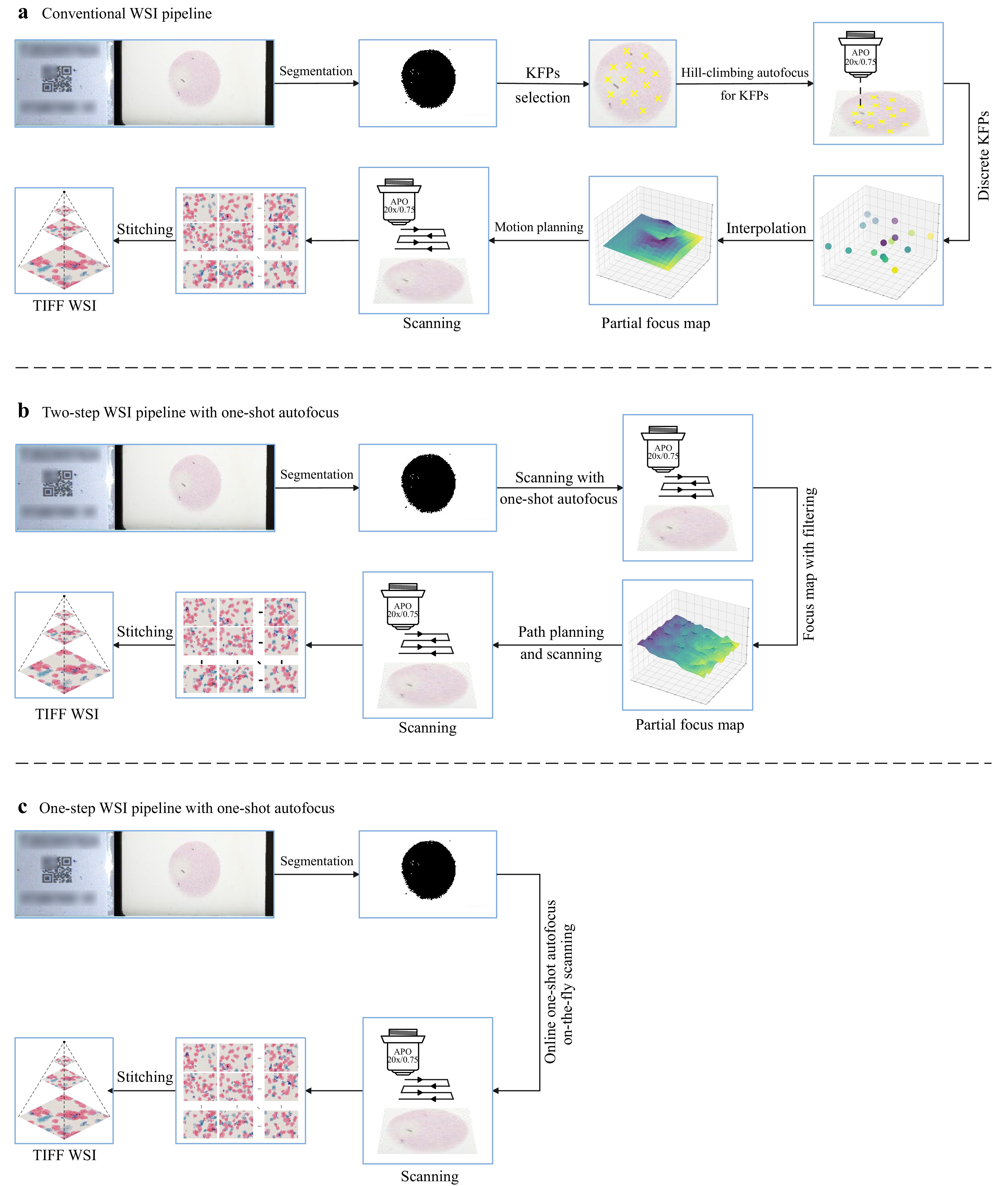
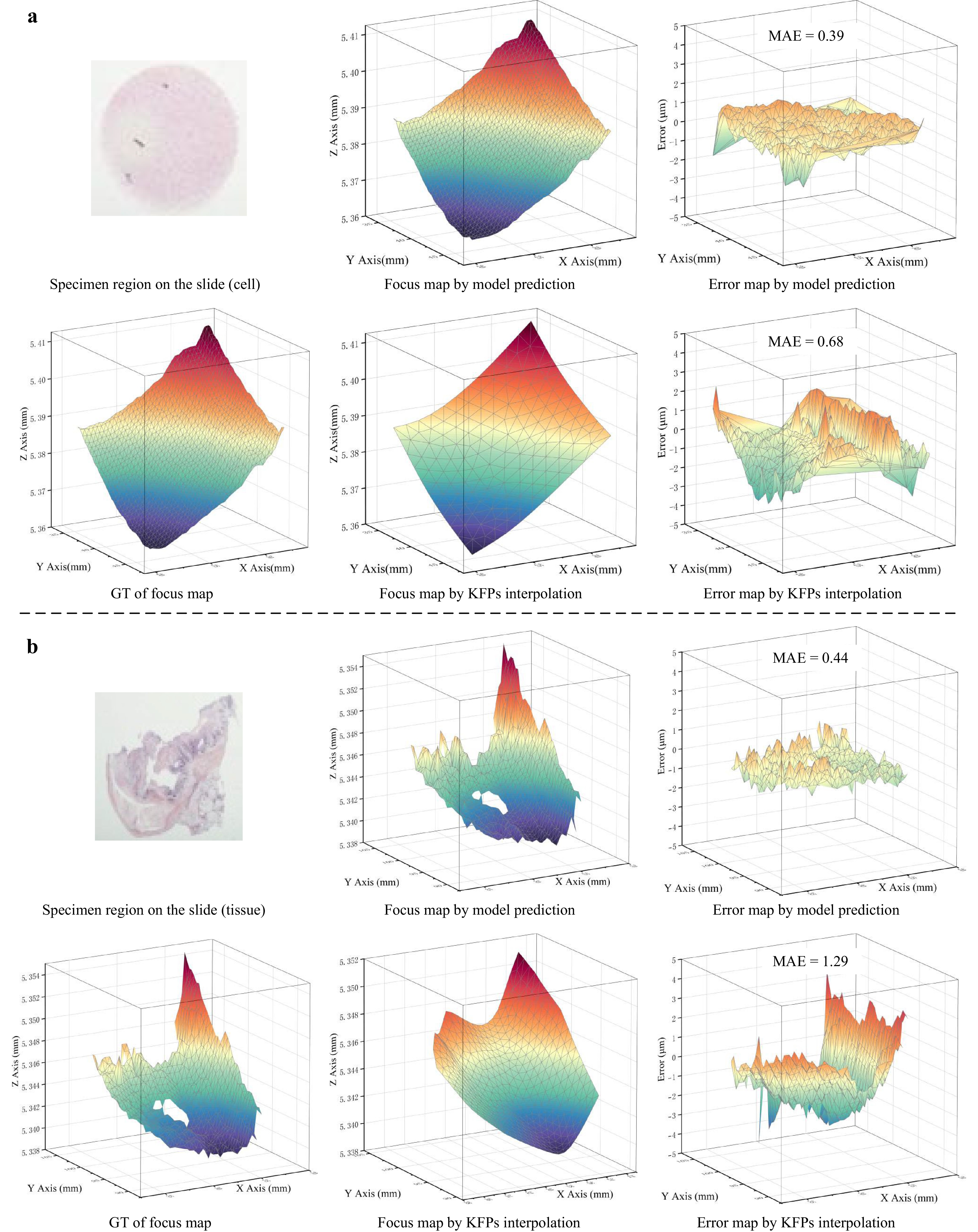
Autofocus is essential for high-throughput real-time scanning in microscopic imaging. Traditional methods rely on complex hardware or iterative hill-climbing algorithms. Recent learning-based approaches exhibited remarkable efficacy in one-shot settings, circumventing the need for hardware modifications or iterative mechanical lens adjustments. However, in this study, we highlight a significant challenge wherein the richness of the image content can significantly affect autofocus performance. When the image content is sparse, previous autofocus methods, whether traditional hill-climbing or learning-based, tend to fail. To address this limitation, we propose a content-importance-based solution, termed "SparseFocus", featuring a novel two-stage pipeline. The first stage assesses the importance of the regions within the image, whereas the second stage calculates the defocus distance from the selected important regions. This approach can handle autofocus issues across all levels of content sparsity (dense, sparse, or extremely sparse). To validate our approach and benefit the research community, we acquire a large-scale dataset comprising millions of labelled, defocused images encompassing dense, sparse, and extremely sparse scenarios. The experimental results demonstrate that SparseFocus surpasses existing methods, effectively handling all levels of content sparsity. Moreover, we develop an advanced one-shot autofocus-enhanced whole-slide imaging system (osa-WSI) based on SparseFocus, coupled with an efficient image-stitching protocol for large-scale imaging and online motion path planning. The system demonstrates strong performance in real-world applications. All codes and datasets will be released upon publication.
Published. 2026, 7(1)
: 60-68
doi: 10.37188/lam.2026.029
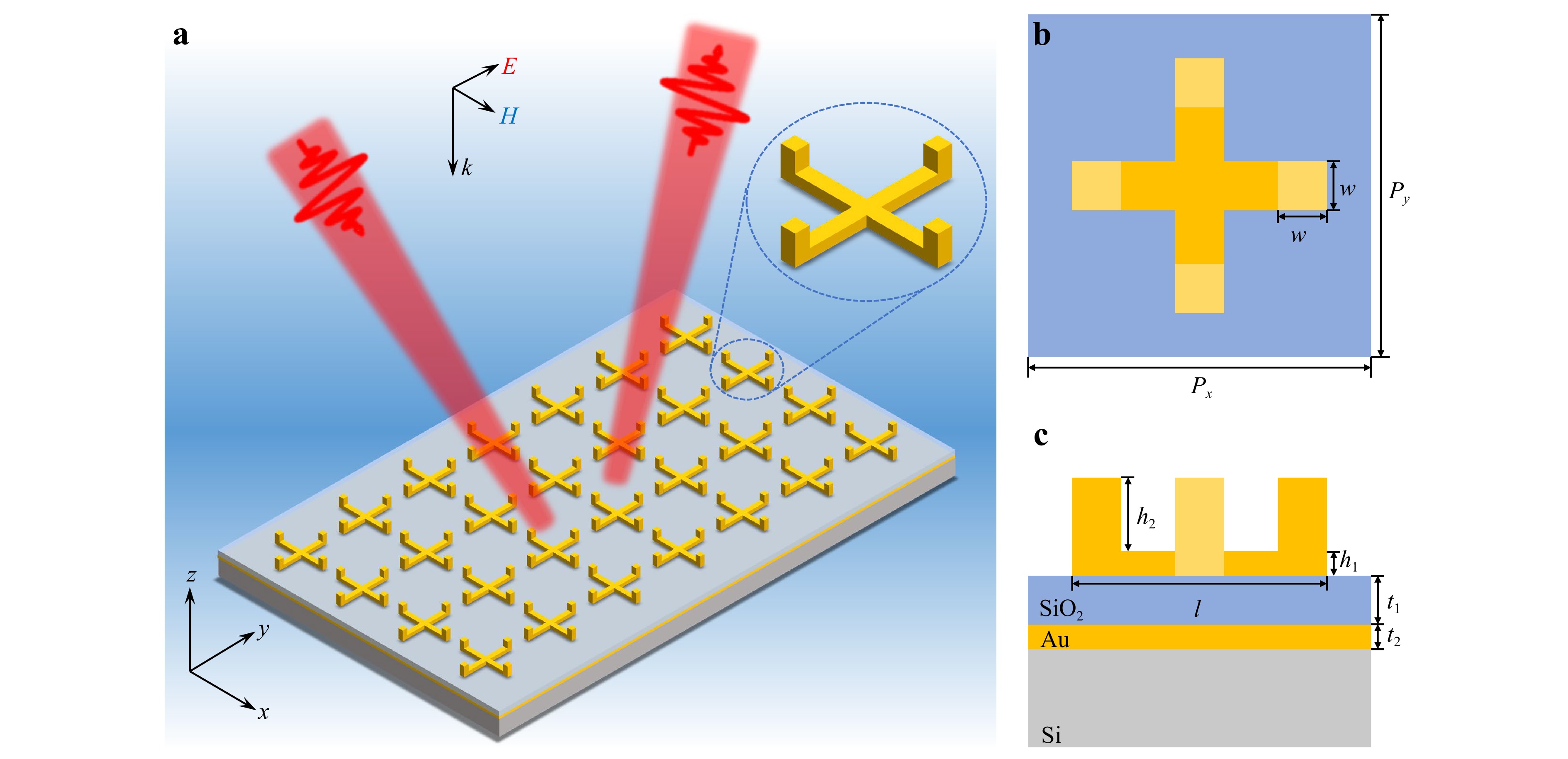
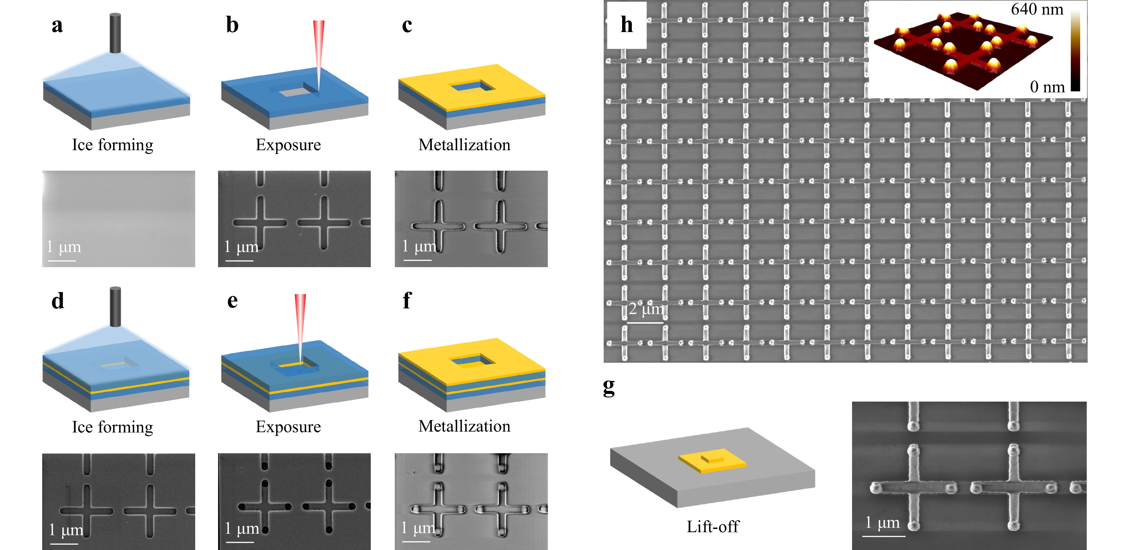
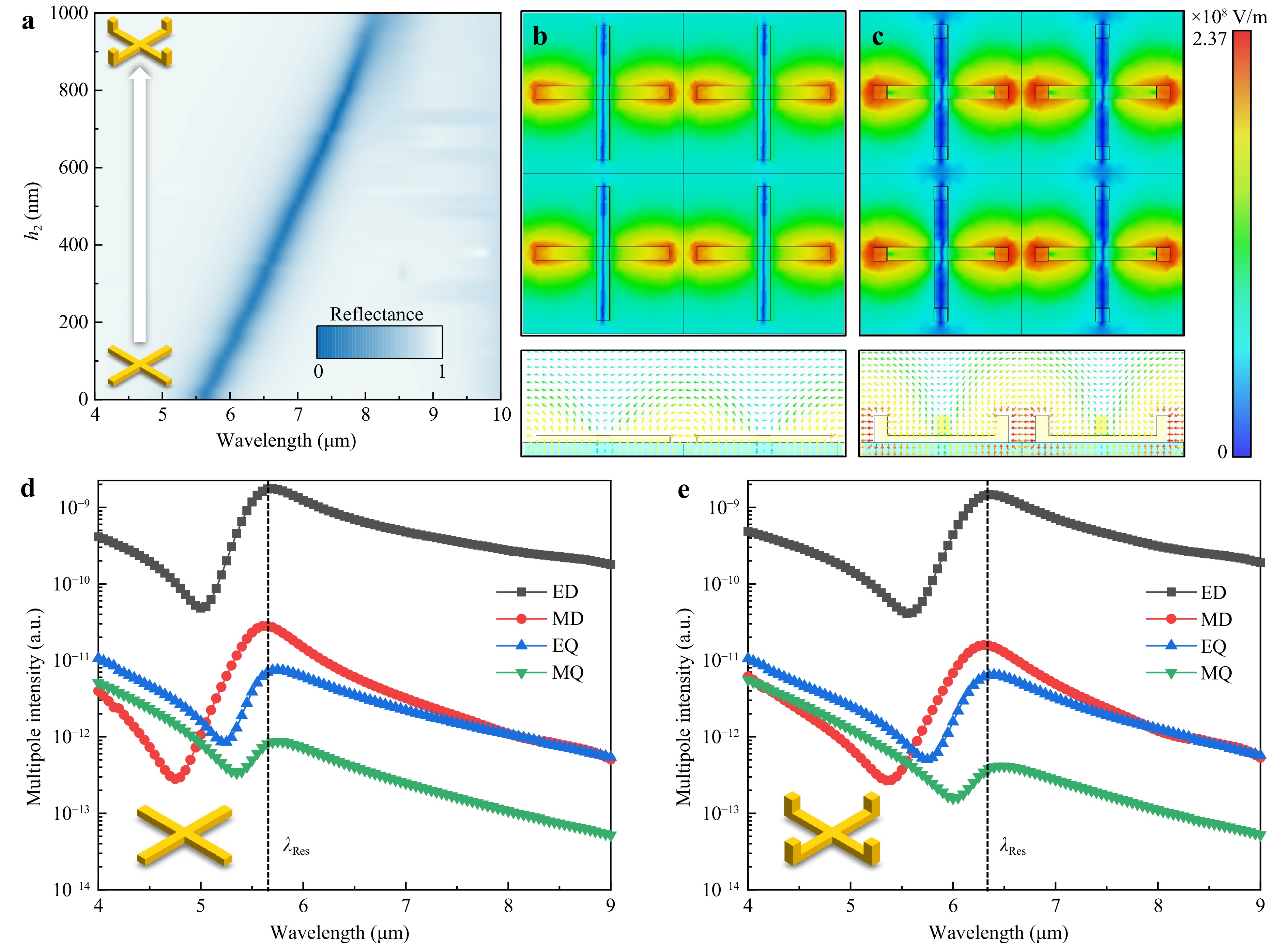
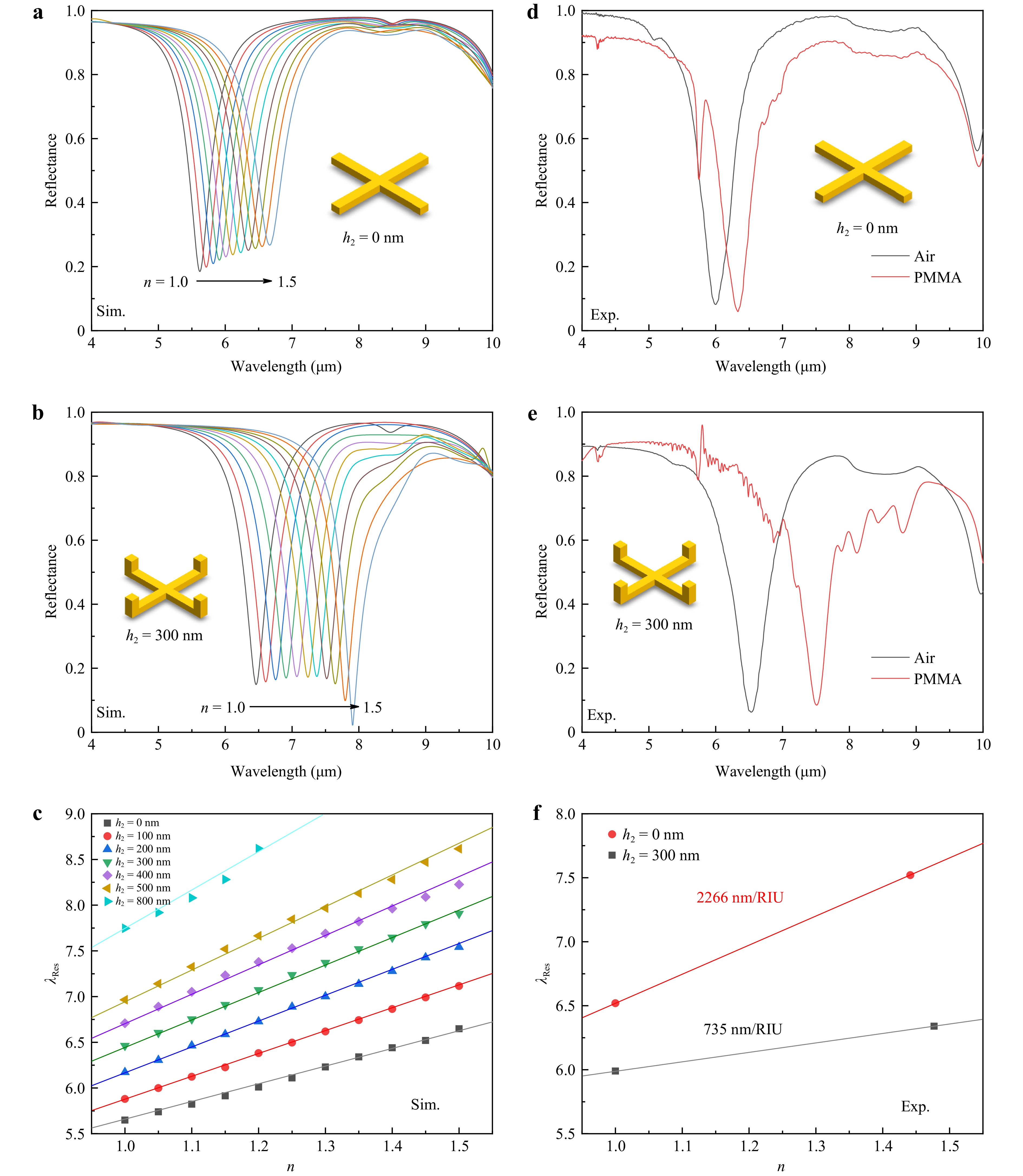
Mid-infrared (MIR) refractive index (RI) sensing holds significant potential for applications in chemical detection, environmental monitoring, and biomedical diagnostics due to the strong molecular vibrational fingerprints in this spectral range. However, conventional metasurface-based sensors face challenges in fabrication complexity, toxic solvents, and performance optimization. Here, we introduce ice-lithographed 2.5-dimensional (2.5D) plasmonic metasurfaces featuring vertically asymmetric gold cross-pillar resonators to overcome these challenges. The solvent-free ice lithography enables in situ scanning electron microscopy (SEM) alignment with high precision, residue-free surfaces, and multilayer stacking in a single vacuum process. Simulations reveal that vertically graded pillars (height 0–800 nm) linearly redshift resonance wavelengths while concentrating electric fields at analyte-binding sites, boosting experimentally measured sensitivity from 735 nanometers per refractive index unit (nm/RIU) to 2 266 nm/RIU. This work demonstrates a three-dimensional (3D) architectural strategy for enhancing sensing performance, while simultaneously unveiling the potential of ice lithography in fabricating low-toxicity and flexible 2.5D sensing devices.
Published. 2026, 7(1)
: 69-86
doi: 10.37188/lam.2026.002
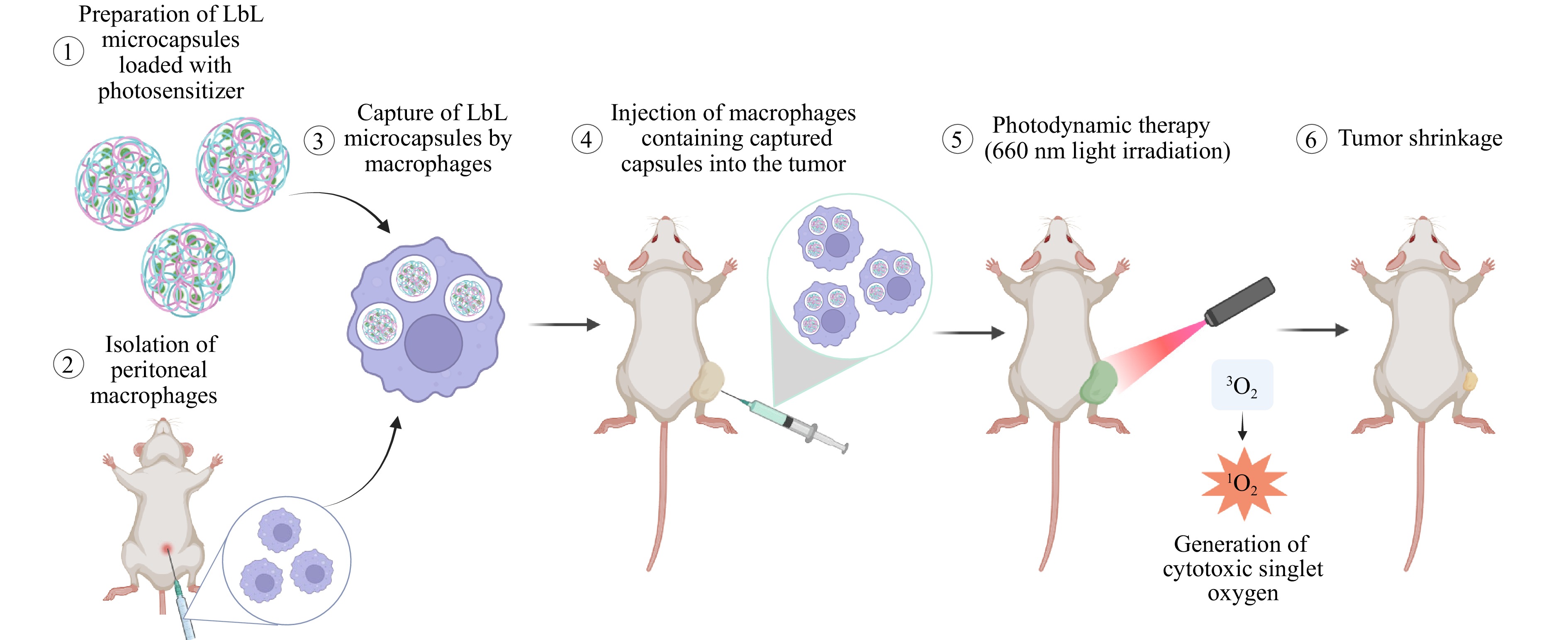
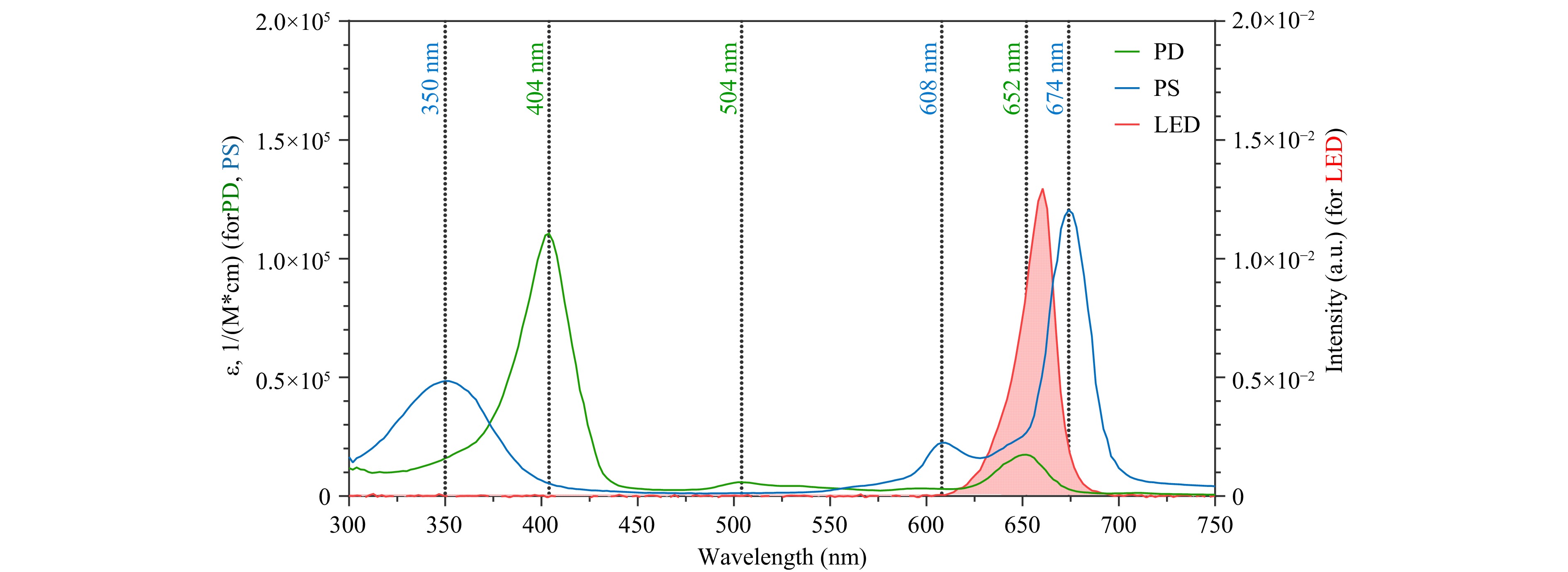
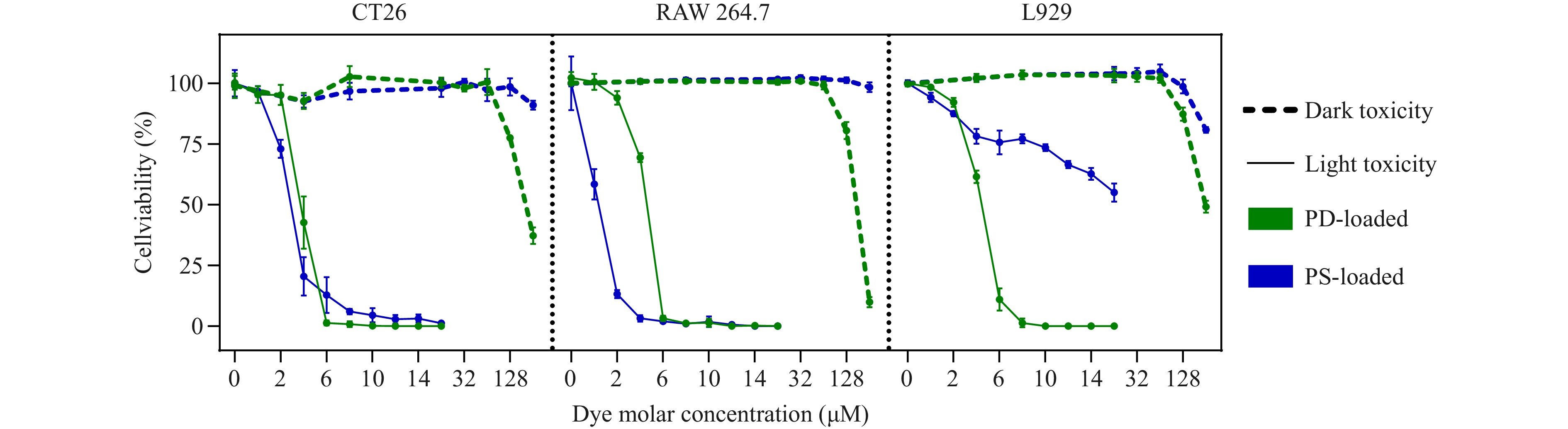
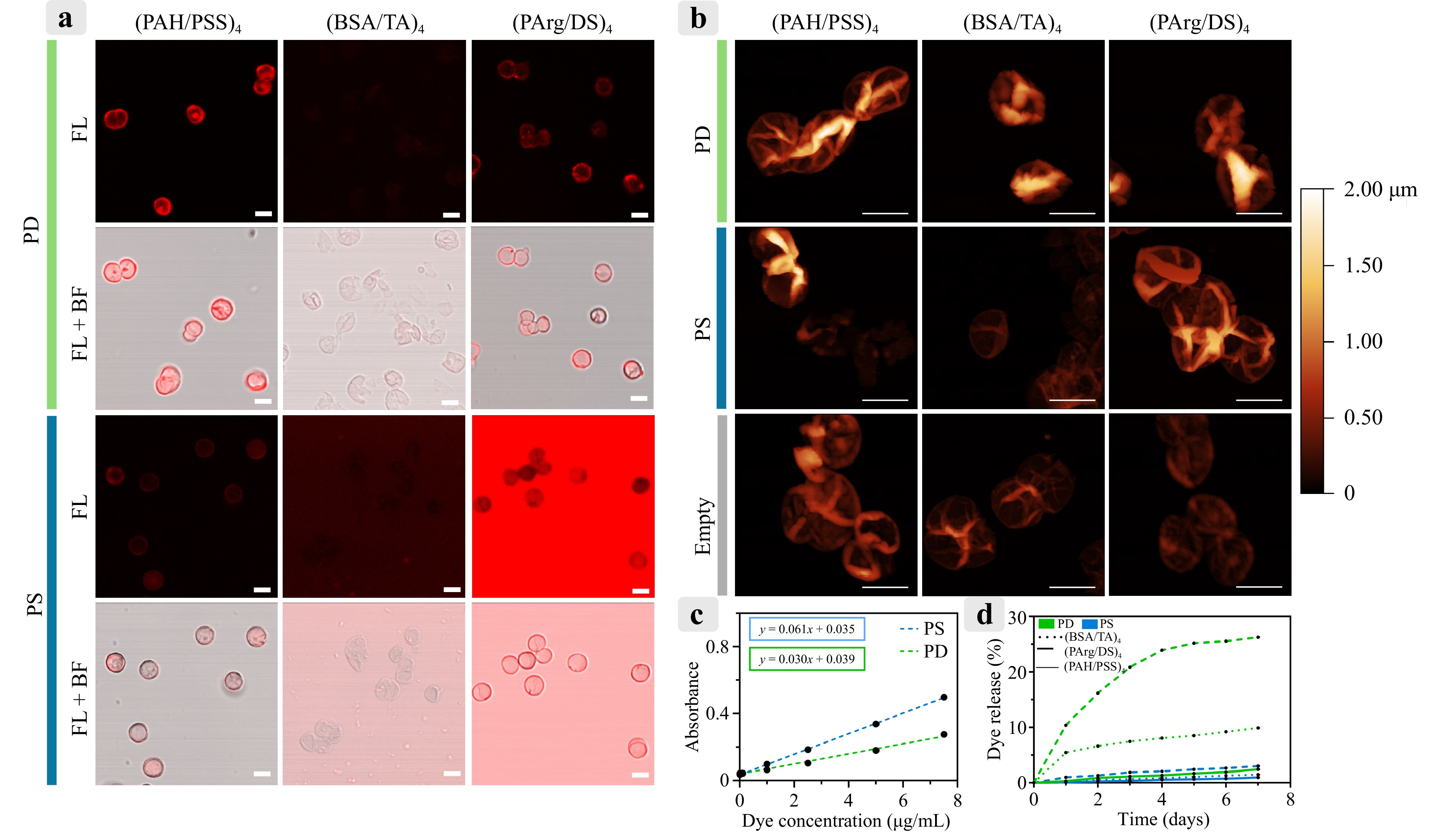
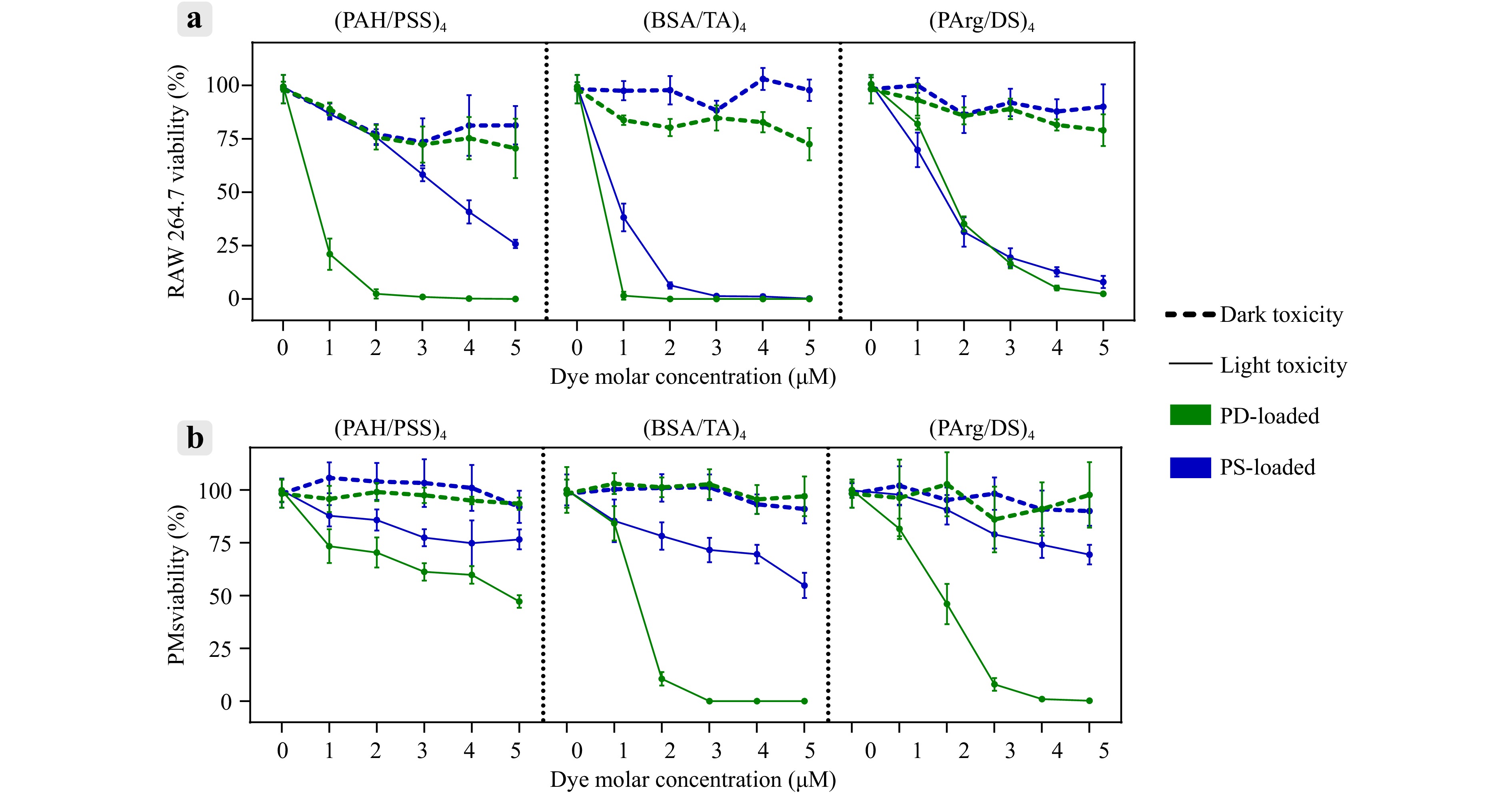
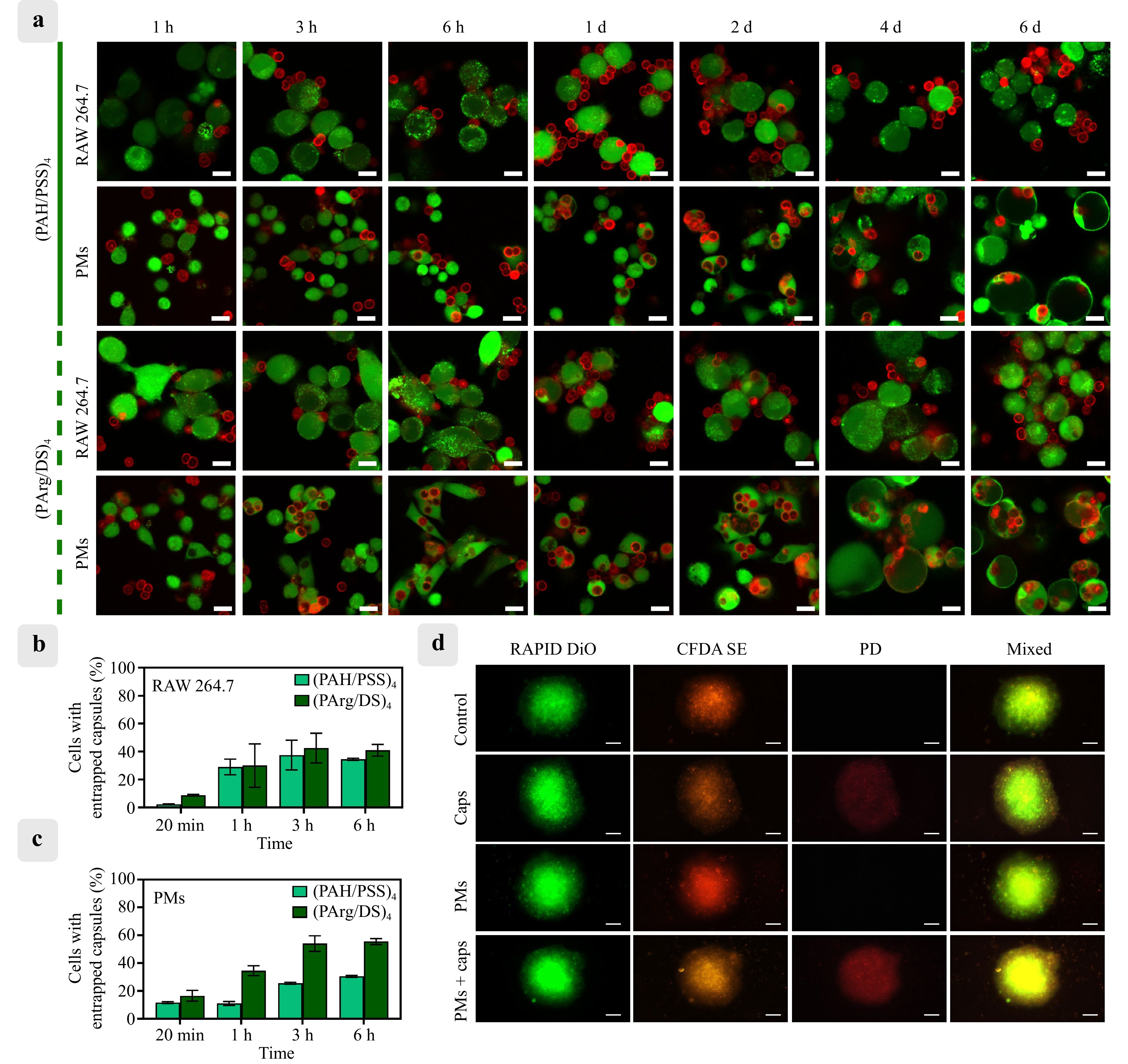
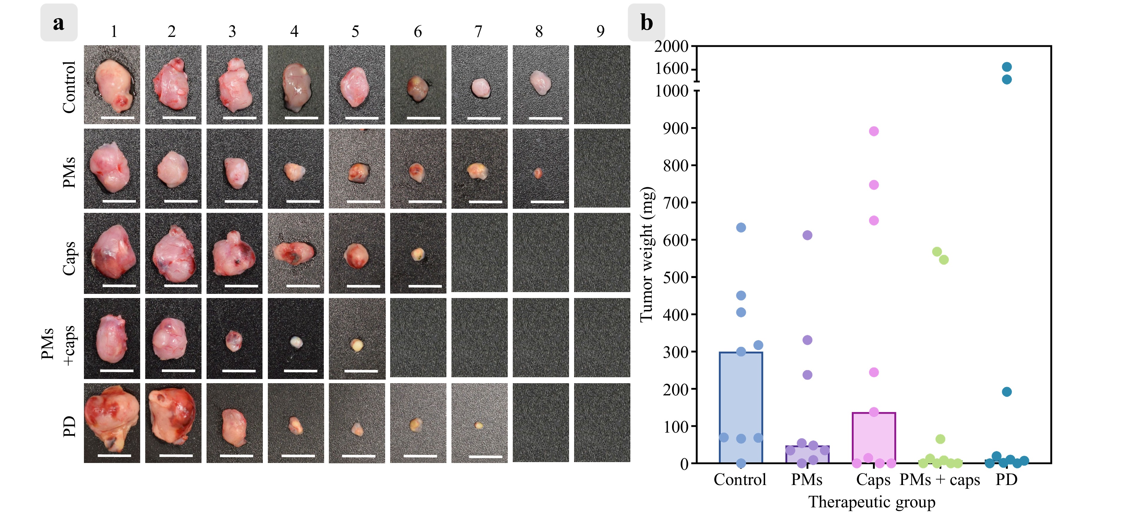
Photodynamic therapy (PDT) is a promising strategy for treating solid tumours due to its spatially controlled, light-triggered cytotoxicity. Although recent advances in optical technologies have improved light delivery, PDT efficacy remains limited by insufficient drug accumulation in tumours, largely due to the complexity of the tumour microenvironment. To address this challenge, a macrophage-mediated delivery platform was developed using layer-by-layer (LbL) microcapsules loaded with second-generation photosensitizers: photoditazine (PD) and aluminum tetrasulfophthalocyanine chloride (PS). Both photosensitizers exhibited low dark toxicity and high phototoxicity, enabling their safe transport by carrier cells. The photosensitizers were efficiently encapsulated into LbL microcapsules (6.2 ± 0.5 μm) with different shell compositions. Significant differences were observed between macrophage types: RAW 264.7 macrophages predominantly retained capsules on the cell surface, whereas primary peritoneal macrophages (PMs) internalised capsules within 3 h and retained them for up to 6 d without degradation. Among the tested formulations, polyarginine/dextran sulfate ((PArg/DS)4) capsules loaded with PD demonstrated the highest uptake efficiency and supported macrophage migration into tumour spheroids. In vivo experiments using a CT-26 colon cancer model confirmed the therapeutic potential of this platform, while highlighting the need for further optimisation for large tumours. This study provides new insights into cell-mediated delivery systems and underscores their potential to enhance PDT outcomes beyond current limitations.

Published. 2026, 7(1)
: 87-100
doi: 10.37188/lam.2026.008
Additive manufacturing of glass with submicron resolution remains challenging due to the intrinsic hardness, brittleness, and weak light absorption of most glasses. Here, we demonstrate the laser-induced forward transfer (LIFT) of substoichiometric solid-state silicon oxide (SiOx, x < 2) films for precise glass-on-glass printing. Using single-pulse 248 nm UV excimer laser irradiation and a custom-designed compression system, we achieve submicron donor−receiver gaps, enabling clean and crack-free transfer onto transparent substrates such as fused silica and borosilicate glass (BK7). In particular, the direct printing of SiOx onto fused silica substrates presents considerable challenges due to their high surface hardness and sensitivity to thermal stress. These factors often lead to poor adhesion and fragmentation of the transferred layers in conventional LIFT setups. We overcome these issues by implementing near-zero gap conditions and optimizing the laser fluence relative to the film thickness, enabling stable, residue-free transfer of SiOx onto fused silica. Systematic analysis reveals a strong dependence of transfer quality on both layer thickness and laser fluence, identifying a critical minimum thickness (~200 nm) and a narrow optimum fluence window. Furthermore, we use this approach to fabricate high-quality binary phase masks (BPMs) directly on glass, which exhibit well-defined π phase shifts and efficient diffraction under HeNe laser illumination. Post-deposition thermal oxidation transforms the transferred SiOx into fully transparent SiO2, making the structures suitable for UV optical applications. The resulting components demonstrate excellent mechanical robustness and resistance to standard cleaning procedures. This work establishes a solid-state pathway for fabricating functional glass-based micro-optical elements via LIFT.


Published. 2026, 7(1)
: 101-110
doi: 10.37188/lam.2026.007
Nanobubbles are typical nanodefects commonly existing in two-dimensional (2D) van der Waals materials such as transition metal dichalcogenides, especially after their transfer from growth substrate to target substrates. These nanobubbles, though tiny, may significantly alter the local electric, optoelectronic, thermal, or mechanical properties of 2D materials and therefore are rather detrimental to the constructed devices. However, there is no post-processing method so far that can effectively eliminate nanobubbles in 2D materials after their fabrication and transfer, which has been a major obstacle in the development of 2D material based devices. Here, we propose a principle, called laser optothermal nanobomb (LOTB), that can effectively flatten nanobubbles in 2D materials through a dynamic process of optothermally induced phase transition and stress-pulling effect in nanobubbles. Operation of LOTB on monolayer molybdenum disulfide (1L-MoS2) films shows that the surface roughness can be reduced by more than 70% on a time scale of ~50 ms, without damage to the intrinsic property of 1L-MoS2 as validated by micro-nano photoluminescence and Raman spectroscopy. Moreover, a dual-beam cascaded LOTB and a multi-shot LOTB strategies are proposed to increase the flattened area and processing effect, showing the potential of LOTB for fast nanodefect repairing in the mass production of van der Waals materials and devices.


Published. 2026, 7(1)
: 111-127
doi: 10.37188/lam.2026.003
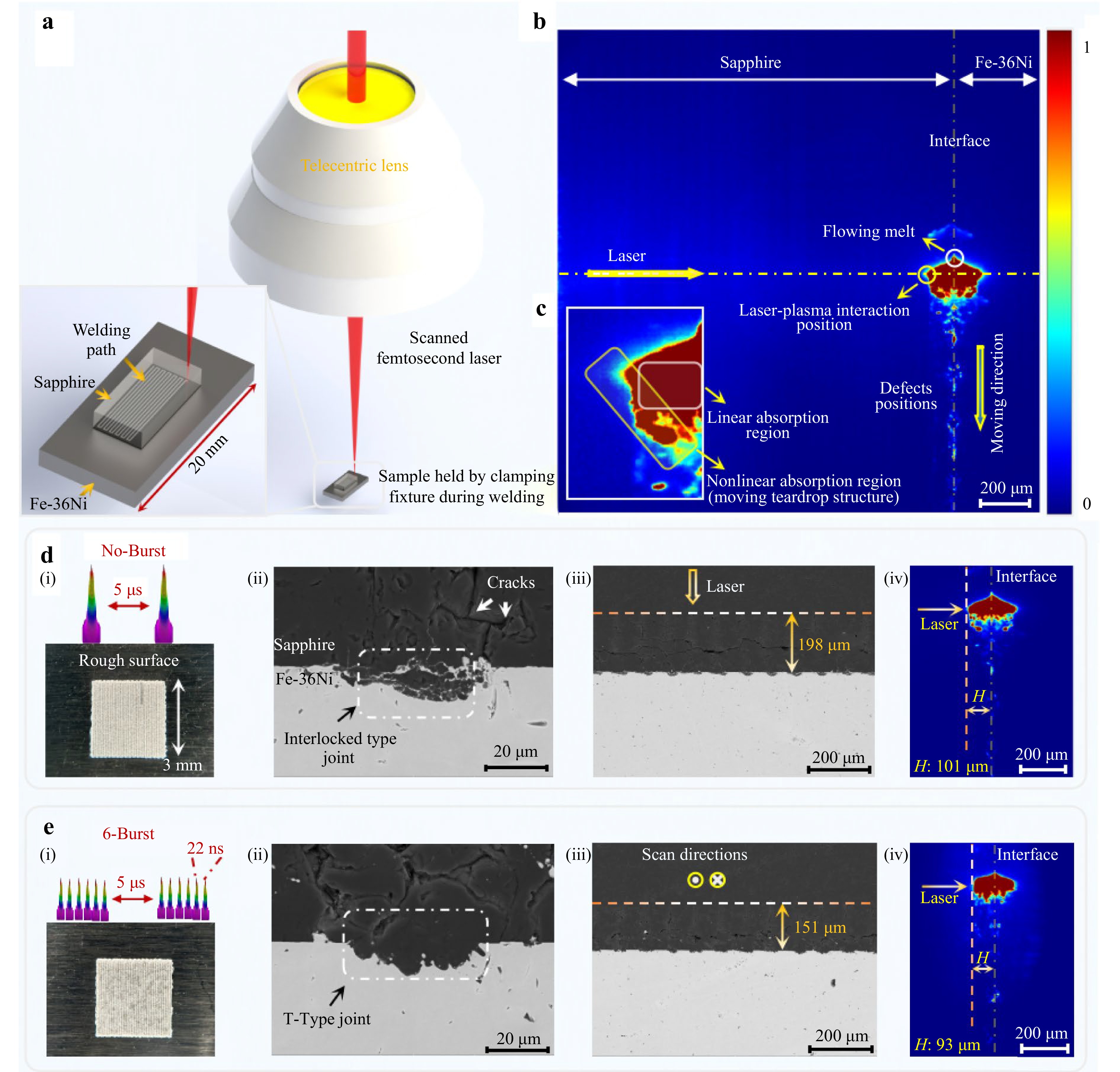
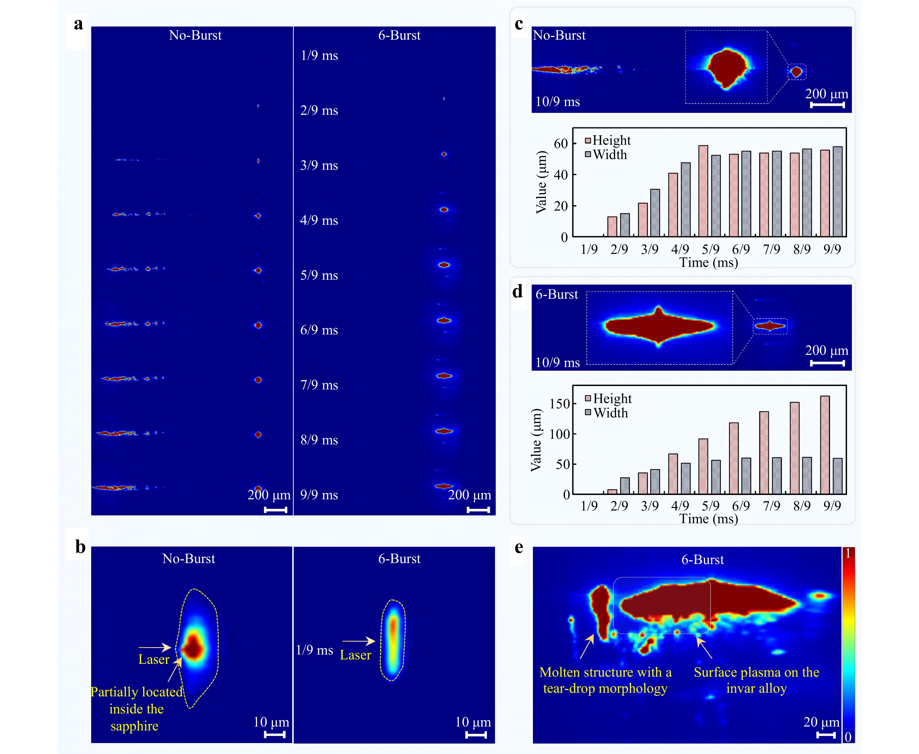
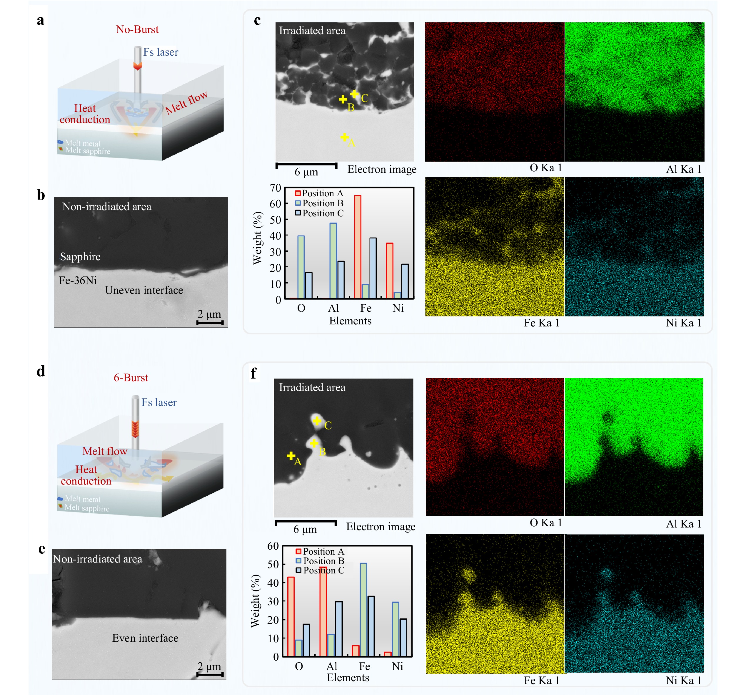
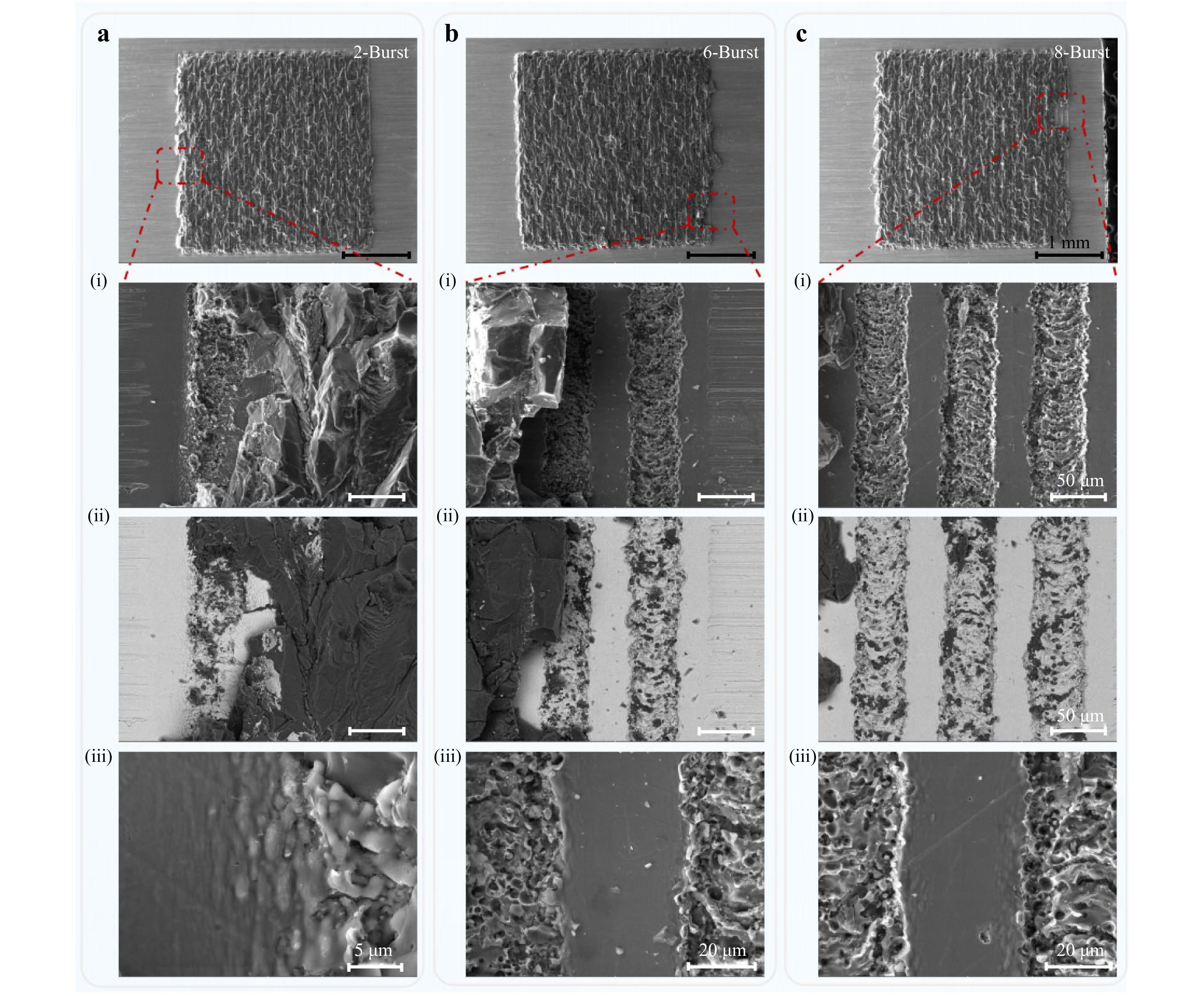
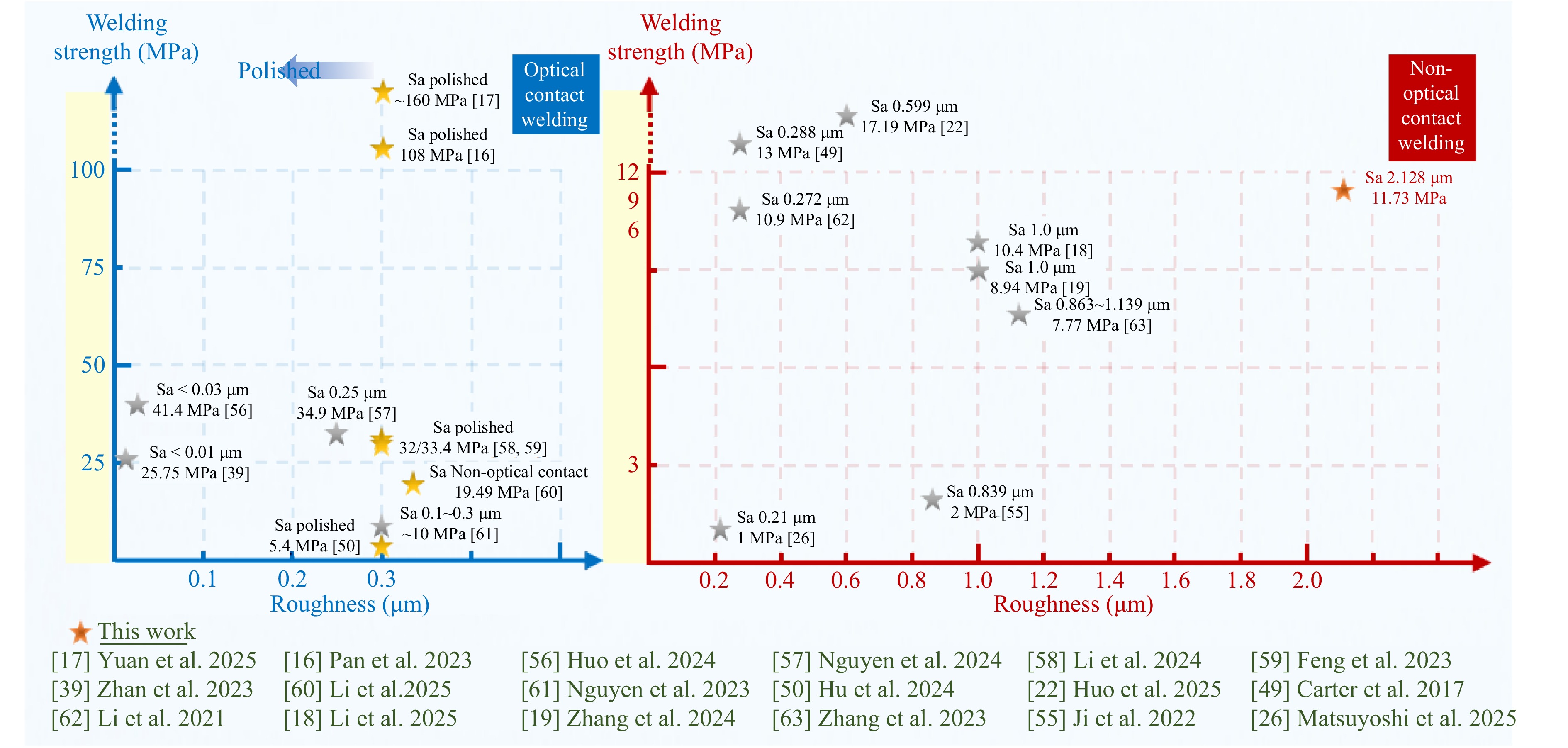
The efficient and robust joining of transparent metal-dissimilar materials remains a significant challenge in high-performance system integration. A primary barrier is the inherently rough surfaces of metals, which hinder reliable bonding with transparent materials, largely due to the limited understanding of the underlying welding mechanisms. In this study, we demonstrate ultrafast laser joining between sapphire and metal substrates with surface roughness (Sa) up to 2 μm, achieving a maximum shear strength of 11.73 MPa. High-speed imaging techniques were employed to conduct the first systematic investigation of coupled absorption dynamics at heterogeneous interfaces. The plasma ejection observed during welding indicated that the molten metal actively confined the interfacial region, transforming the initial free space into a confined space. This transition facilitates the formation of an optical contact condition, significantly improving the joint strength. To further explore the potential of pulse shaping in controlling interfacial behaviour, the effects of temporal shaping (Burst mode) on laser energy deposition, joint strength, and interfacial morphology were examined. Consistent joint quality was achieved across a range of burst parameters, with shear strengths ranging from 9 to 13 MPa. Fractographic analysis indicated that the fracture was predominantly governed by the internal stress within the sapphire, thereby limiting further improvements in joint strength. The revelation of the ultrafast laser welding mechanism for non-optical contact dissimilar materials, along with the exploration of temporal shaping for enhancing welding performance, offers theoretical insights and technical guidance for the development of high-performance heterogeneous material joining.

Published. 2026, 7(1)
: 128-158
doi: 10.37188/lam.2026.035
The relentless pursuit of higher resolution and sensitivity in astronomical observation drives the advancement of telescope mirror manufacturing. This review systematically charts the technological evolution from material innovation to the deterministic control of full-spatial-frequency errors. We analyze the progression of substrate materials—including silicon carbide, beryllium alloys, and advanced glass-ceramics—focusing on their critical thermomechanical properties for extreme environments. The core manufacturing chain is thoroughly examined: ultra-precision diamond turning for initial form generation, grinding processes exploiting brittle-to-ductile transitions, and advanced polishing techniques like magnetorheological finishing and ion beam figuring that achieve nanometer-level accuracy. A central theme is the paradigm shift towards segmented mirrors, which necessitates solving system-level challenges in edge control, co-phasing, and high-consistency batch production. The integration of field-assisted machining and intelligent systems, such as digital twins and robotics, is highlighted as a key enabler for next-generation manufacturing. While significant progress is evident, core challenges persist in stable sub-nanometer finishing, subsurface damage mitigation, and long-term performance under operational extremes. Future development hinges on deeper material-process co-design, fully integrated metrology-manufacturing loops, and sustainable production frameworks. This synthesis provides a comprehensive technical foundation for developing the extreme optical systems required for future discoveries in astrophysics.


Published. 2026, 7(1)
: 159-202
doi: 10.37188/lam.2026.001
Precision aspherical lenses are in high demand for a wide range of industrial and consumer products. While plastic lenses have gained popularity for low cost and flexibility, glass remains the superior material for high-end optics for its exceptional optical properties. Glass molding is a modern manufacturing technique that offers both high precision and affordability. This review, aimed at both academic and industrial communities, provides a brief history of this technology followed by a detailed discussion of the fundamental physics and modeling involved in the molding process. The review also includes a brief discussion of optical design and forming equipment but focuses on the molding process. In addition to conventional methods, we also cover special molding techniques like rapid heating and wafer-level glass molding, as well as the molding of chalcogenide glass lenses. By examining key developments in material modeling, mold fabrication, heat transfer and process optimization, this review aims to support ongoing advancements for next-generation precision optical manufacturing processes.


 Email
Email RSS
RSS