

2026 Vol. 7, No. 3

Published. 2026, 7(3)
: 611-613
doi: 10.37188/lam.2026.085
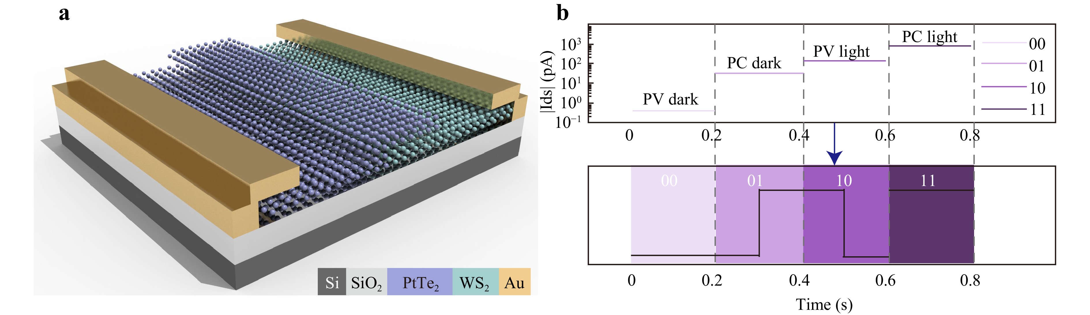
A bias-switchable van der Waals phototransistor demonstrates reconfigurable transitions between photovoltaic and photoconductive modes, generating four current states within a single device. This multi-state functionality advances on-chip optical logic and image encryption. It offers a promising route towards secure, low-power, and highly integrated photonic communication systems.
Published. 2026, 7(3)
: 614-616
doi: 10.37188/lam.2026.119
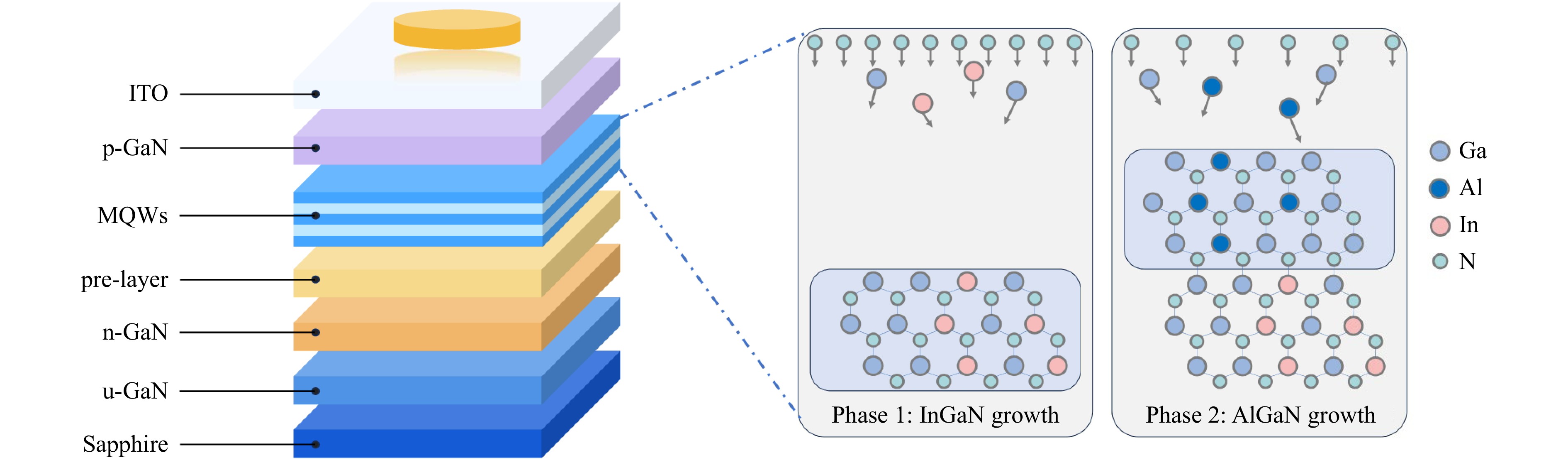
InGaN/AlGaN digital-alloy barriers have enabled weak-polarisation-field III-nitride light-emitting diodes (LEDs) on industrially compatible polar c-plane substrates. By optimising ammonia-flow-modulated pulse growth, this strategy improves digital-alloy interface quality, reduces the polarisation electric field to 0.5 MV/cm, and delivers blue LEDs with a peak external quantum efficiency of 15%. The resulting lateral carrier confinement mitigates sidewall-related efficiency loss, thus offering a practical pathway towards high-performance micro-LEDs.
Microcavity-enhanced optoelectronic fiber photoacoustic spectroscopy for ppb-level trace gas sensing
Published. 2026, 7(3)
: 617-627
doi: 10.37188/lam.2026.028
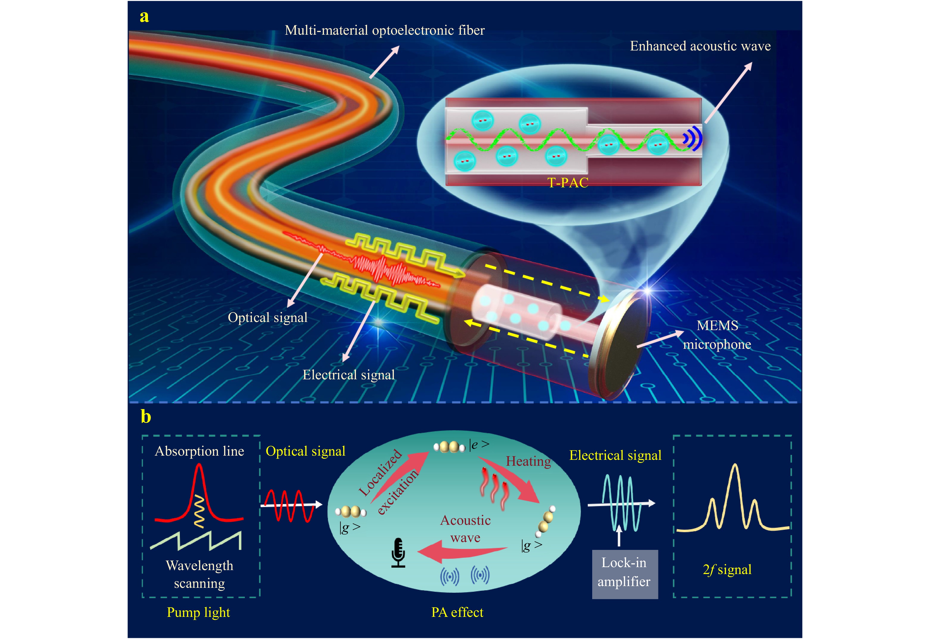
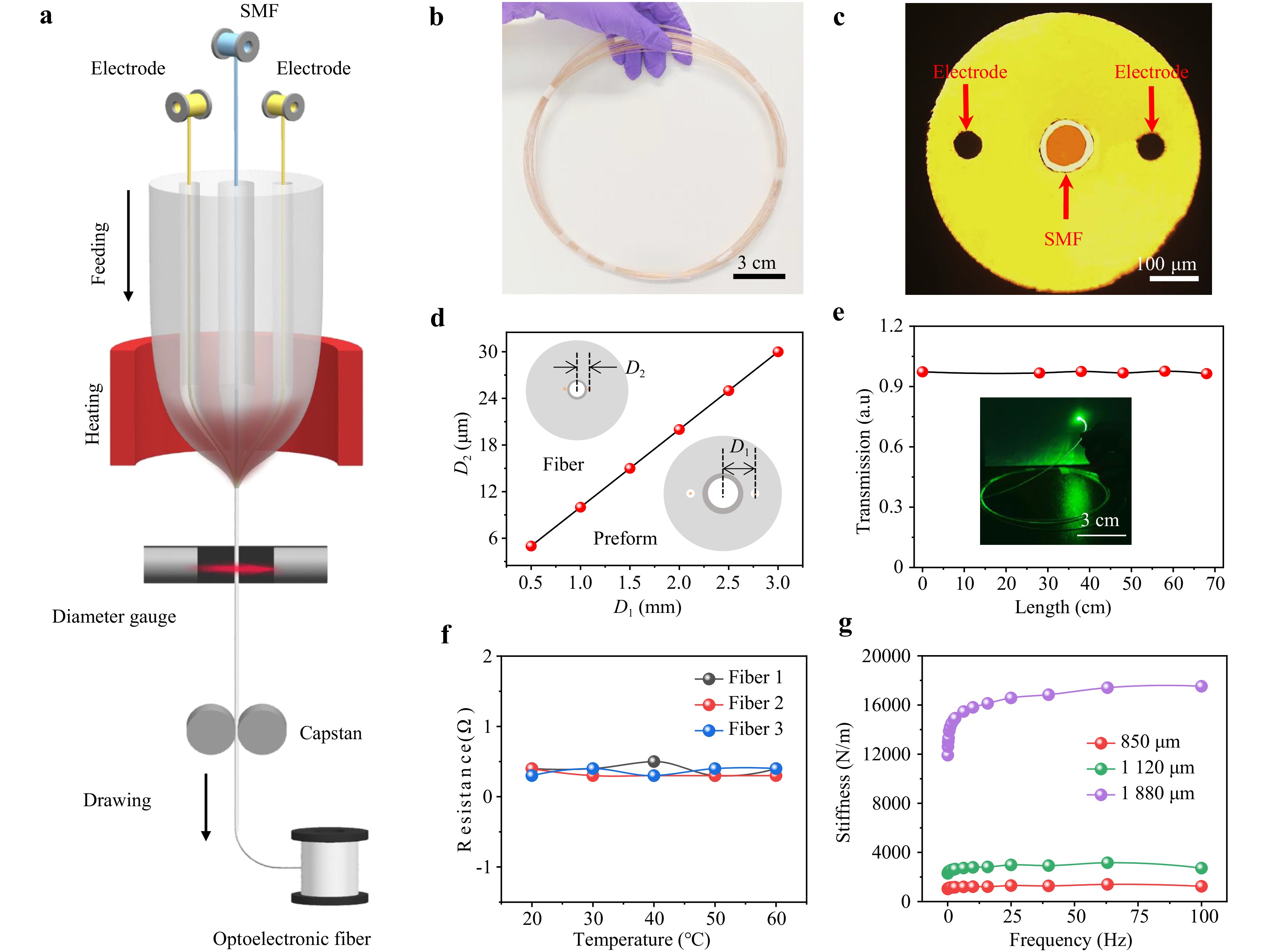
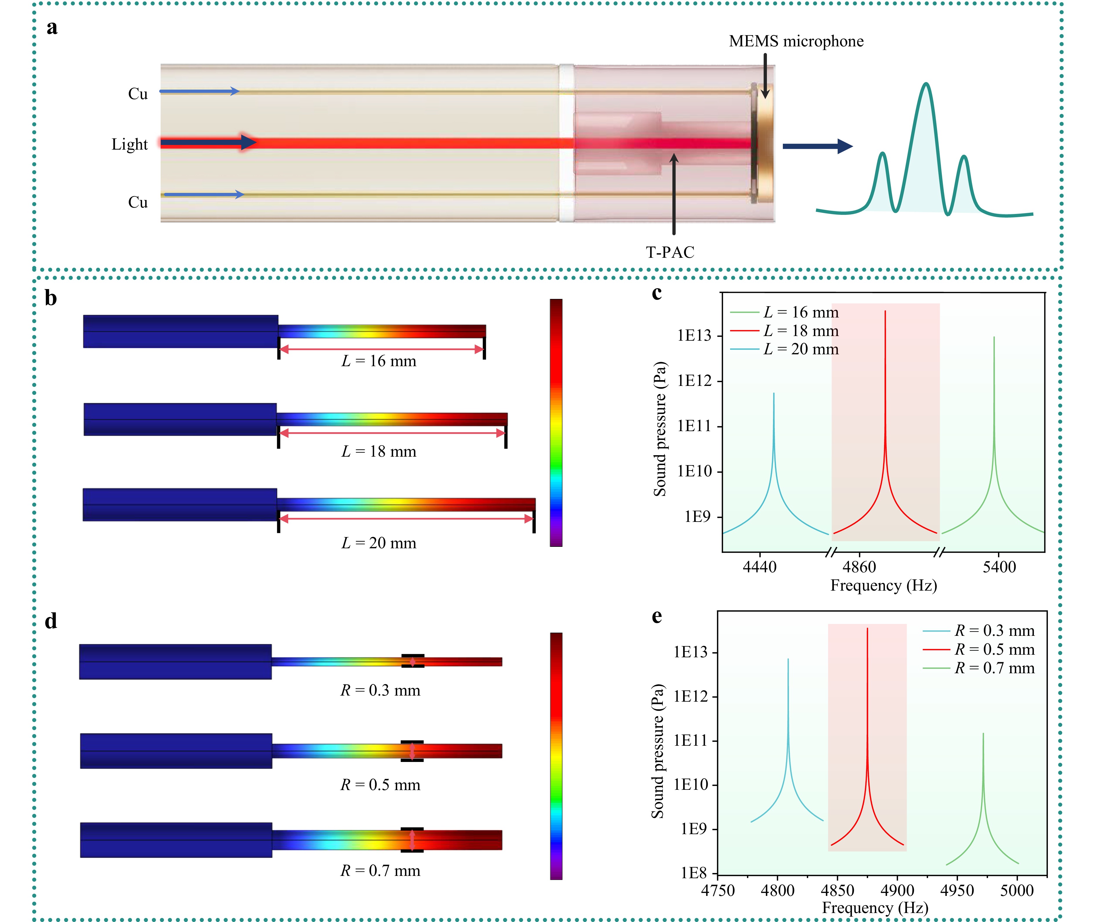
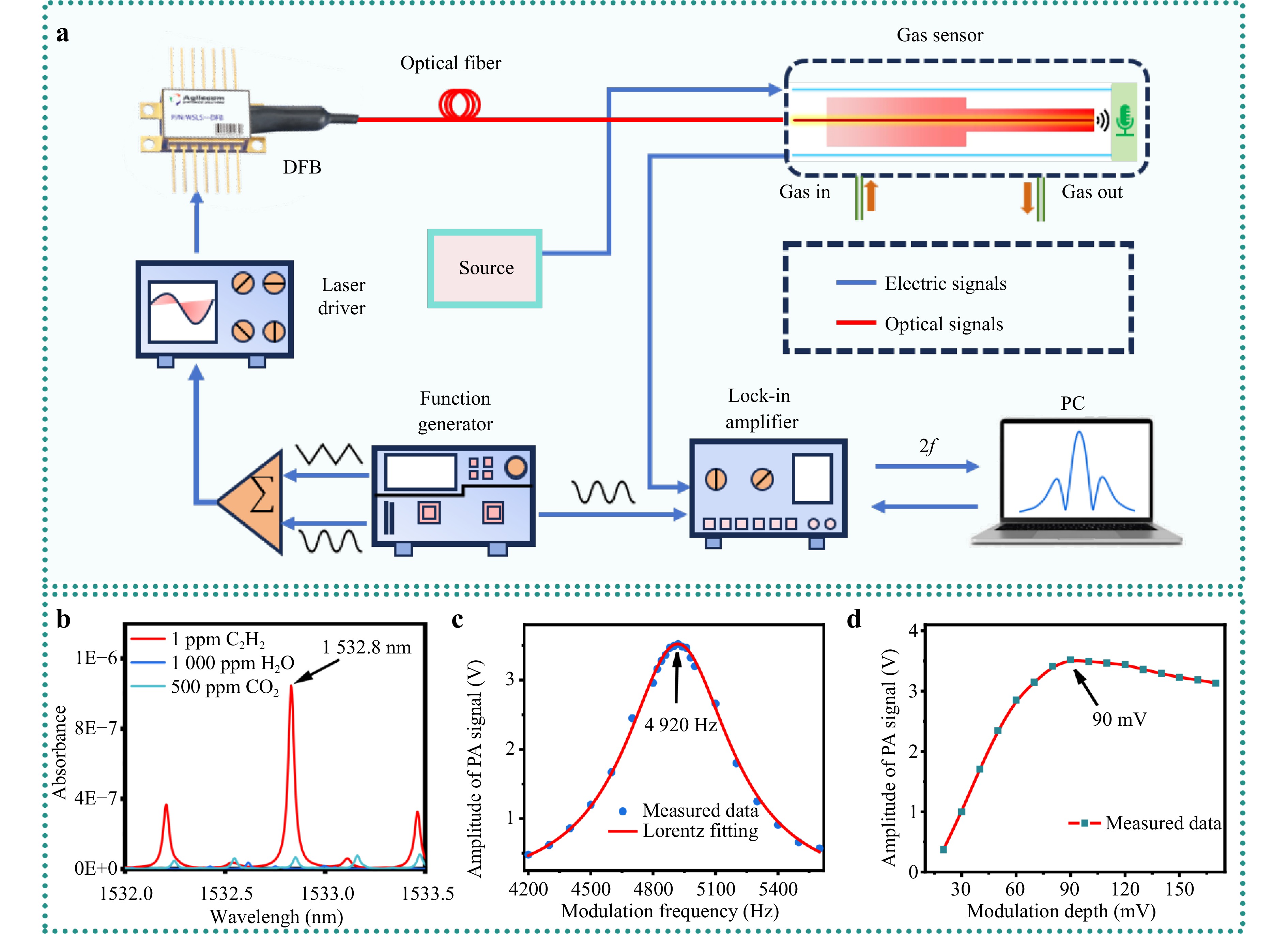
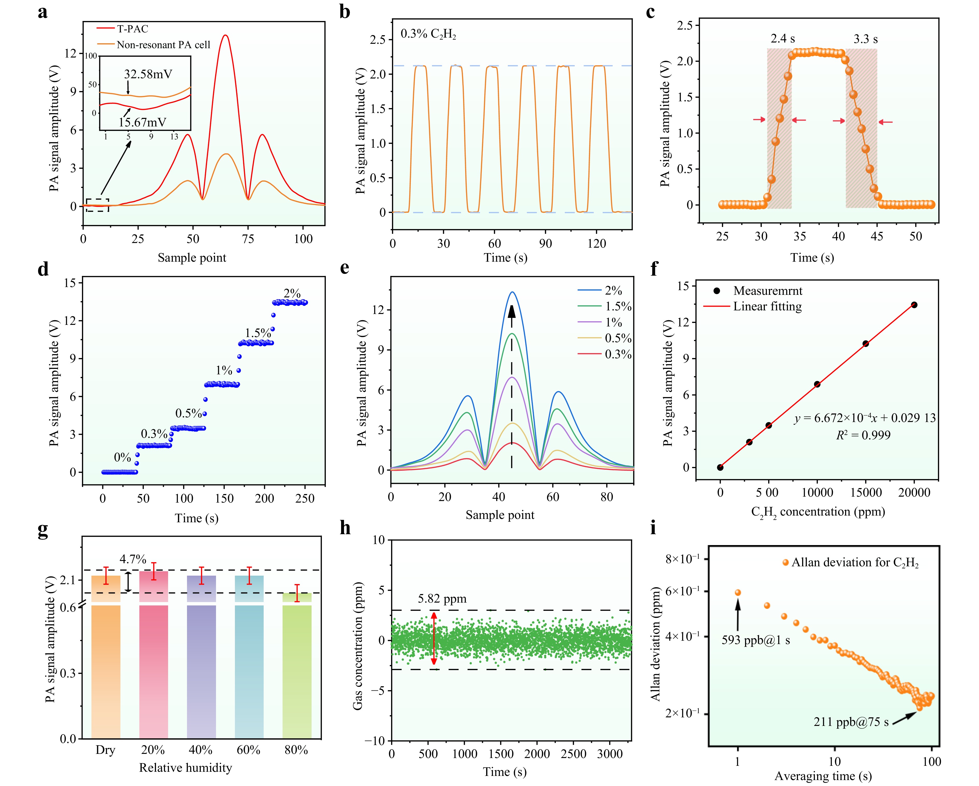
Photoacoustic spectroscopy is a highly sensitive analytical technique for trace chemical detection in gaseous and liquid phases. Conventional systems relying on free-space optics face limitations in light-matter interaction efficiency and electronic integration. To address this, we developed a miniaturized, ultrasensitive photoacoustic spectroscopy gas sensor by integrating a thermally drawn multi-material optoelectronic fiber, a T-type resonant photoacoustic cell, and a MEMS microphone at the fiber tip. This system enables amplified light-gas interactions and simultaneous electrical signal acquisition, achieving ppb-level detection within seconds using sub-microliter sample volumes (0.02 mL). By leveraging mass-producible optoelectronic fibers and MEMS technology, this work establishes a new class of optical sensors featuring compact size, ultrahigh sensitivity, environmental robustness, and scalable multiplexed detection capabilities for harsh environments.
Published. 2026, 7(3)
: 628-637
doi: 10.37188/lam.2026.079
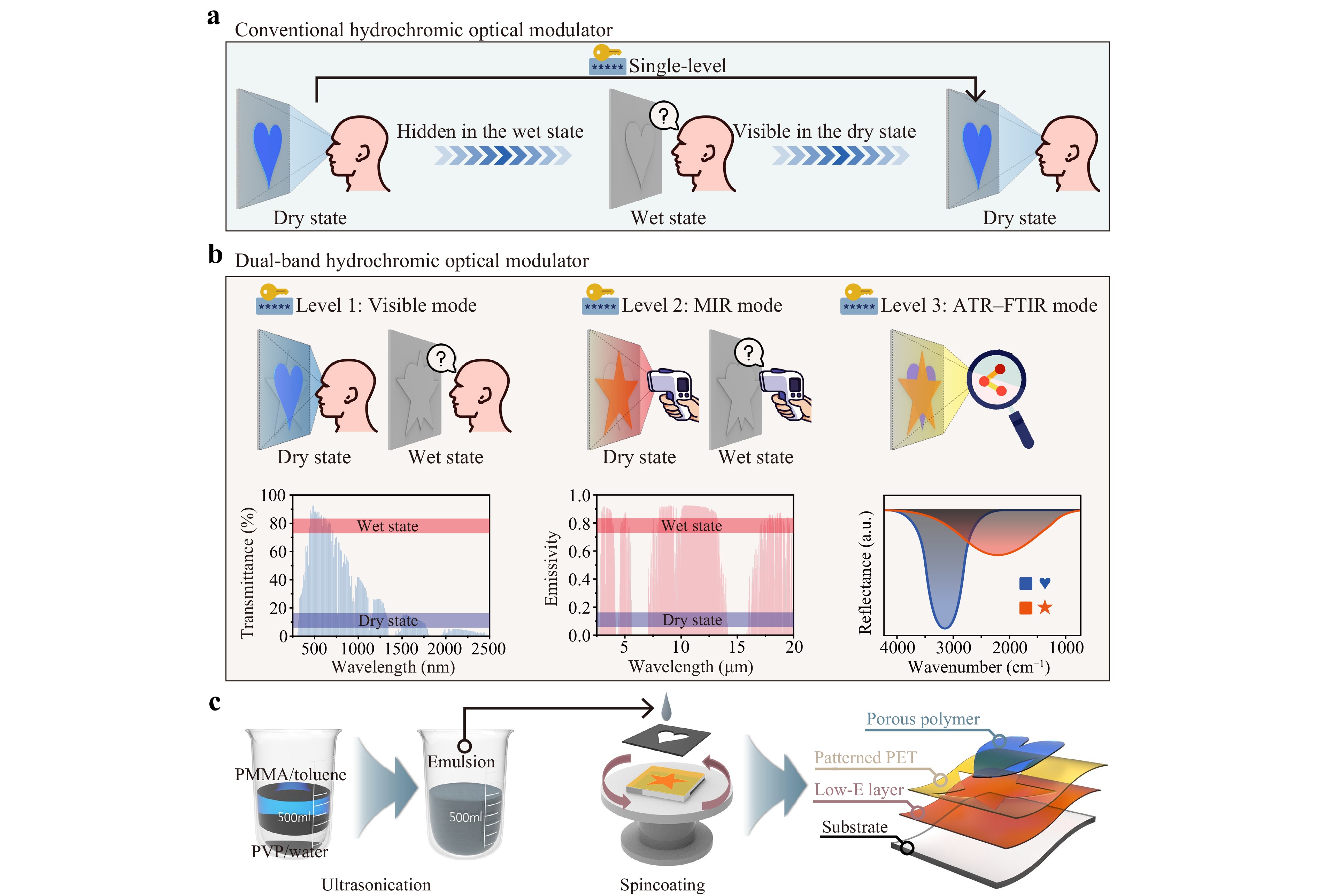
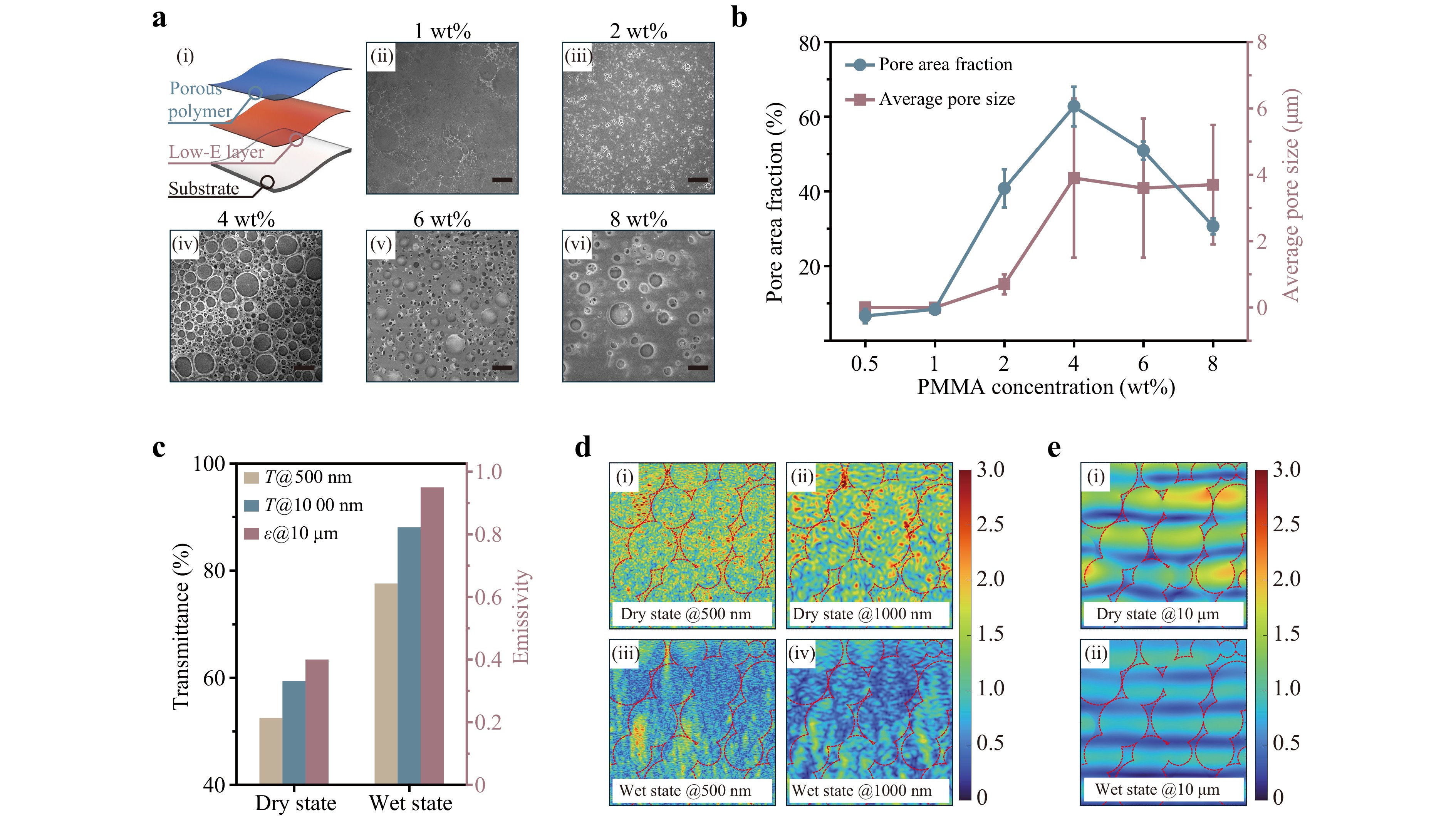
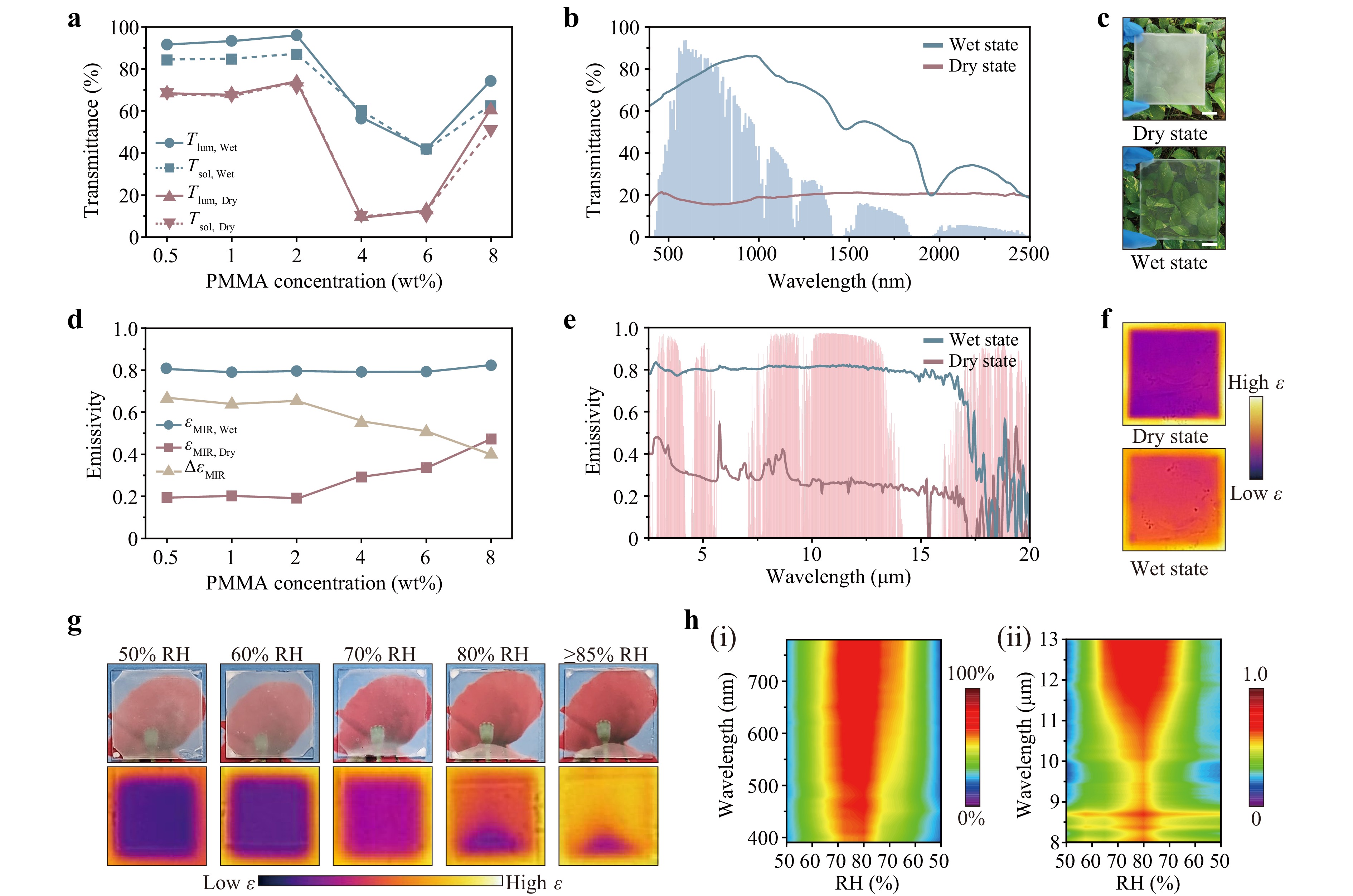
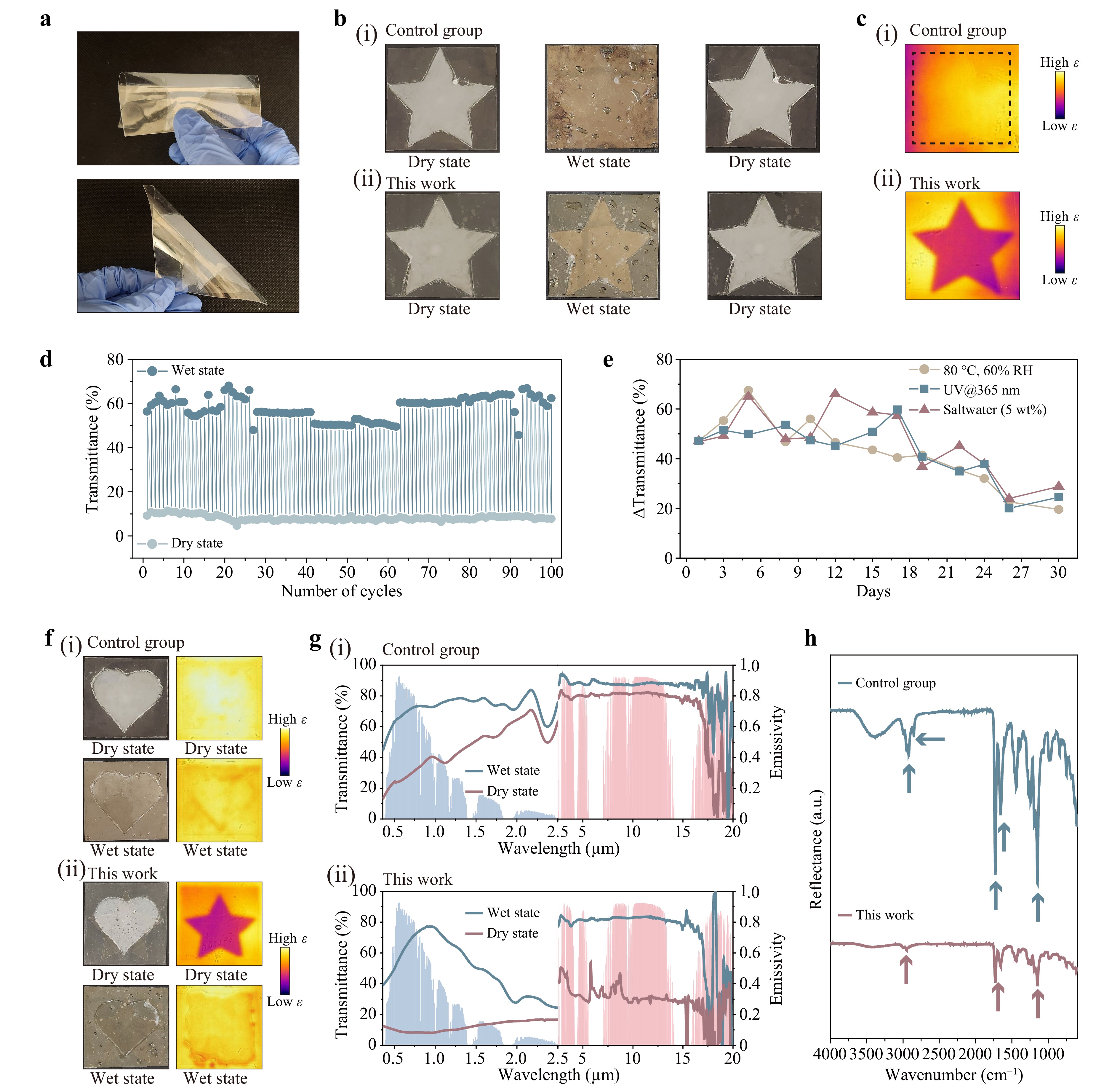
With the rise in digital threats and product counterfeiting, the development of advanced anticounterfeiting and encryption systems has become increasingly critical. Hydrochromic smart materials with dynamically tunable optical responses have emerged as a promising approach for next-generation anticounterfeiting applications. However, the vast majority of reported hydrochromic designs are based on single-band (visible) modulation, rendering them inherently vulnerable to decryption and replication. Herein, we address this challenge through the design of a controlled pore-structured hydrochromic dual-band anticounterfeiting platform, which enables multi-level information encoding across visible, mid-infrared, and attenuated total reflection Fourier-transform infrared modes, thereby enhancing authentication reliability. The platform is fabricated via a scalable and industrially compatible emulsion process and exhibits dry–wet dual-band optical modulation superior to that of the state-of-the-art, achieving up to ~47.2% luminance transmittance modulation and ~0.55 mid-infrared emissivity modulation. Moreover, it demonstrates excellent environmental durability, maintaining stable optical performance after repeated dry–wet cycles and under harsh operating conditions, including high temperature, ultraviolet irradiation, and saltwater exposure, thereby ensuring long-term operational stability. The uniquely engineered hydrochromic dual-band anticounterfeiting platform offers a promising strategy for dynamically tuning optical responses across multiple wavelength regimes, with broad potential applications beyond advanced anticounterfeiting.
Published. 2026, 7(3)
: 638-647
doi: 10.37188/lam.2026.059
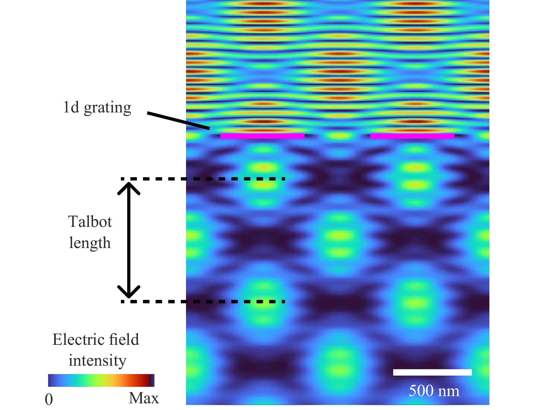
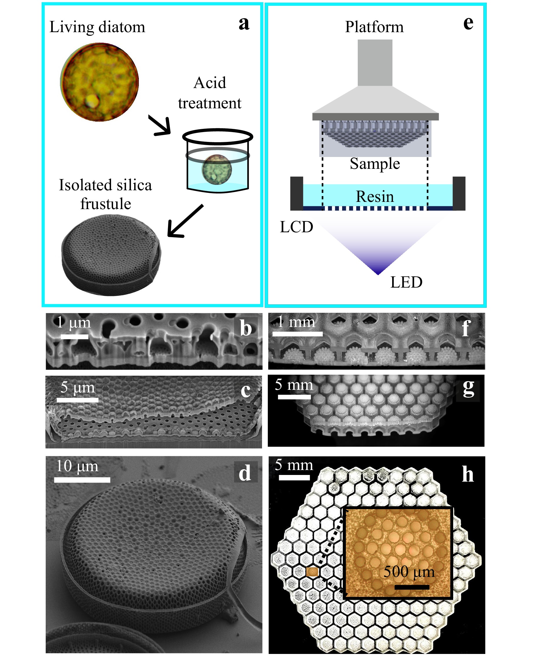
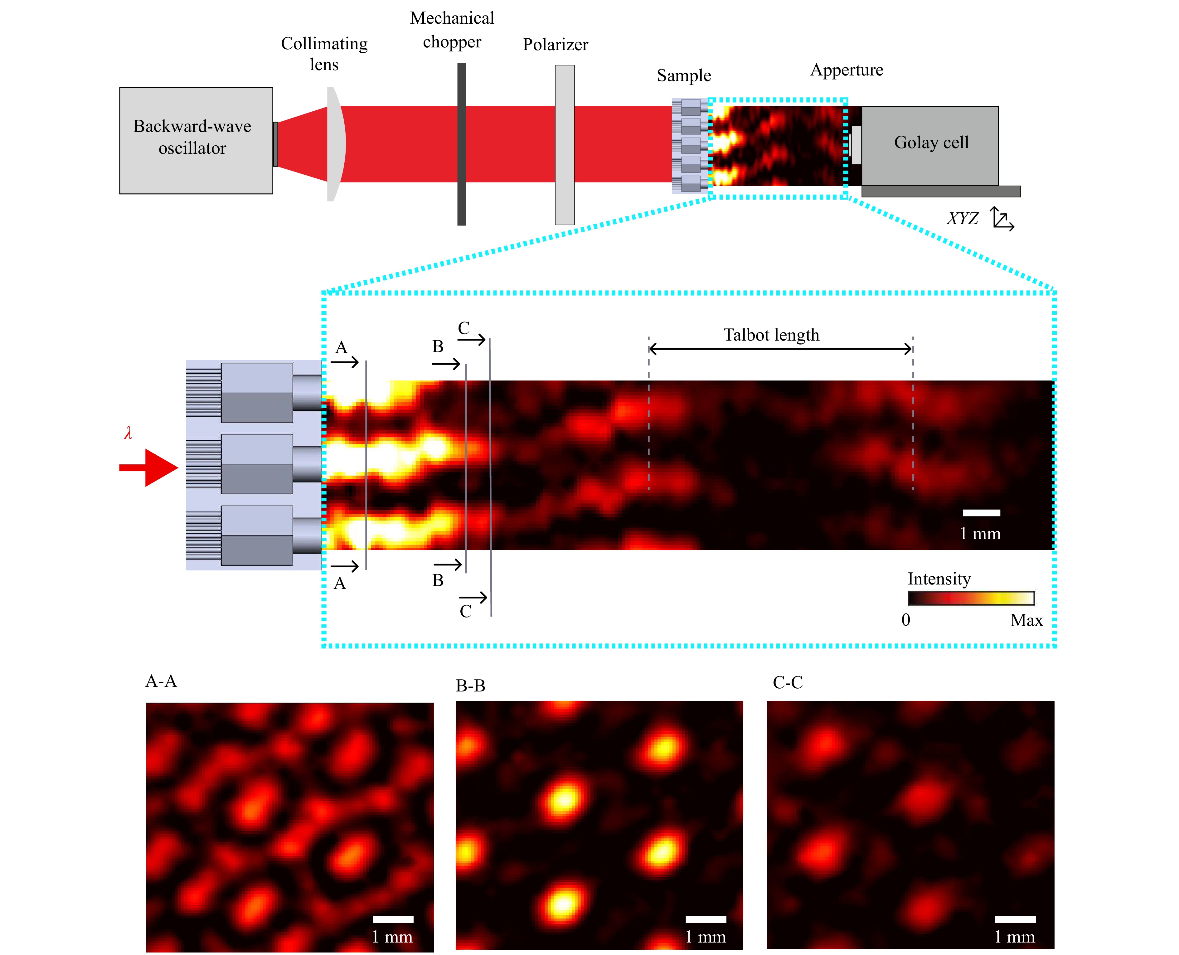
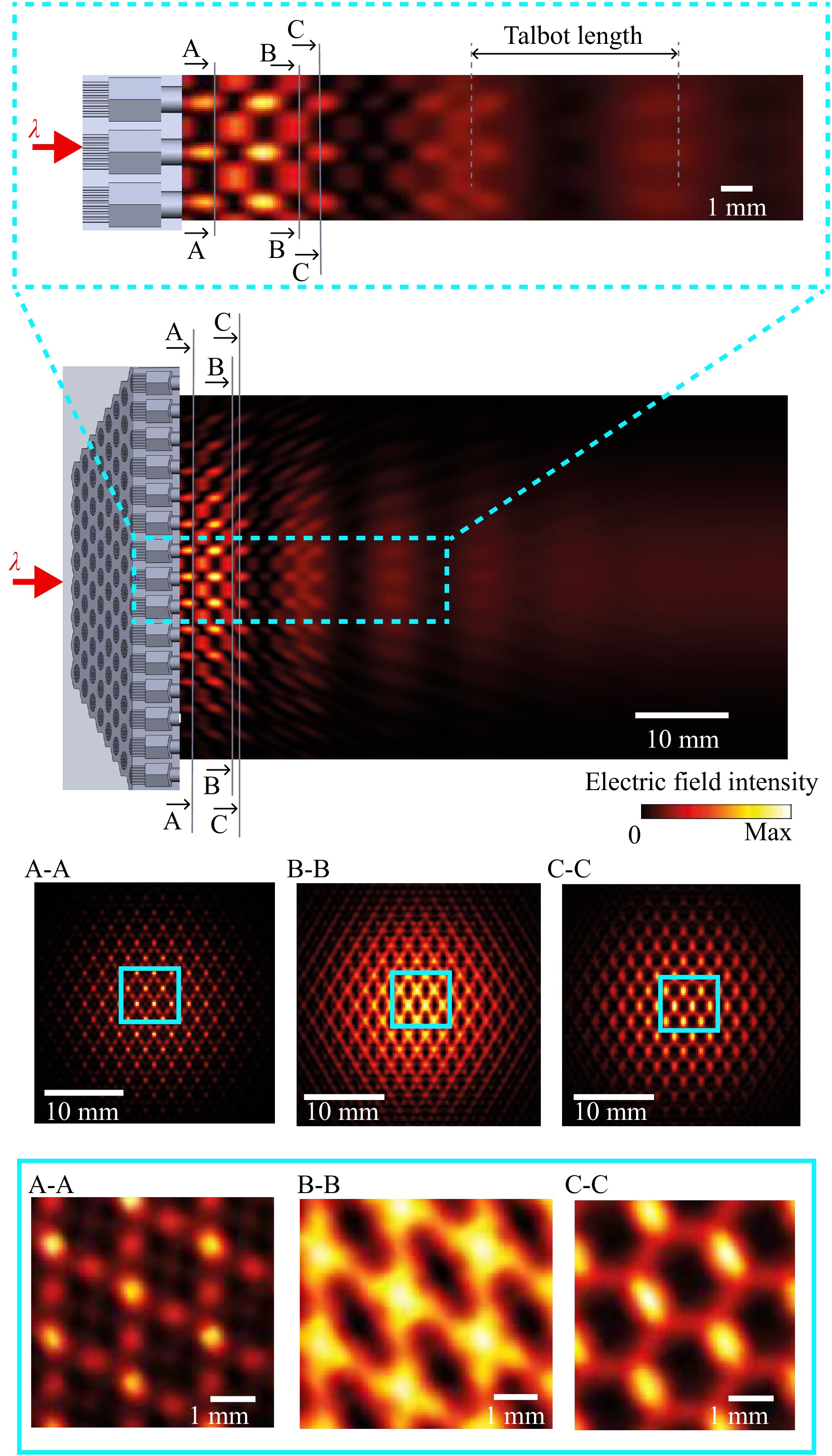
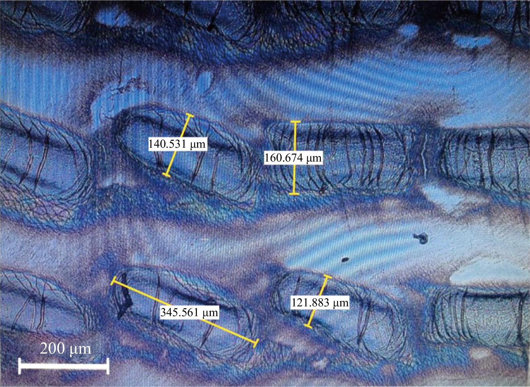
Diatoms are single-celled microalgae with highly ordered nano- and microstructured silicon dioxide shells (silica frustules), which function as natural photonic crystals for efficient light management. One of the predicted optical phenomena in diatom frustules is near-field Talbot interference, which provides localised focusing of incident radiation within a cell. In this work, we employed geometric scaling in the terahertz (THz) regime, where the Talbot distance increases to millimetres, allowing direct visualisation of the longitudinal self-imaging process. Scaled-up biomimetic models of diatom frustules were produced using liquid crystal display (LCD) 3D printing, and optical characterisation was performed at a wavelength of λ = 911 µm. The size of the holes in the structure ranged from 100 µm to 1 mm, corresponding to approximately a 2,000-fold geometric scale-up relative to natural diatom features. At a distance of 4.6 mm from the structure, the intensity at the focal points was half that of the original beam. The experimental results are consistent with numerical simulations carried out using the Fourier modal method. This work demonstrates a bioinspired approach to low-dimensional diffractive photonic structures with controllable optical properties by translating diatom-inspired nanophotonic concepts into manufacturable polymers. The designs obtained provide a scalable route to fabricating THz components that can function as flat focusing optics, tunable resonant filters, and wavefront modulators when integrated into devices. Compatibility with additive manufacturing enables large-scale, cost-effective production by allowing the combination of natural photonic architectures with modern fabrication techniques, thereby supporting applications in photonic systems, light harvesting, and smart sensing.
Published. 2026, 7(3)
: 648-659
doi: 10.37188/lam.2026.054
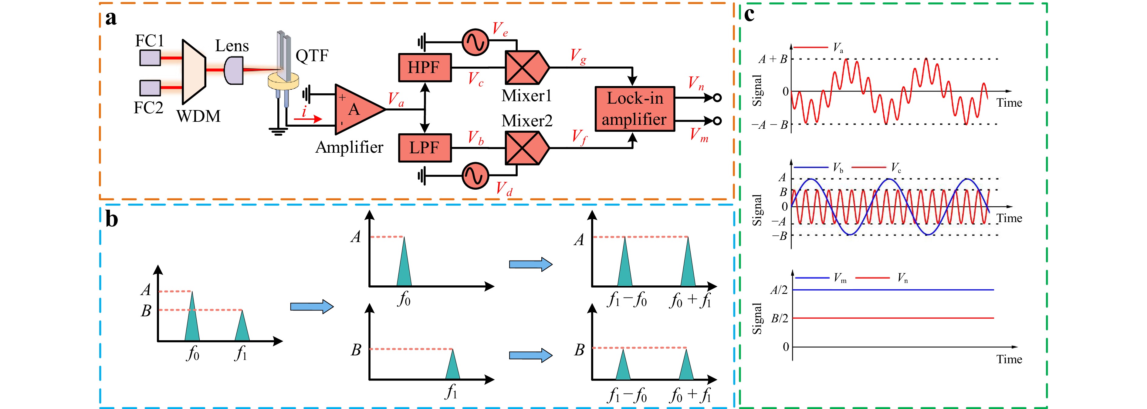
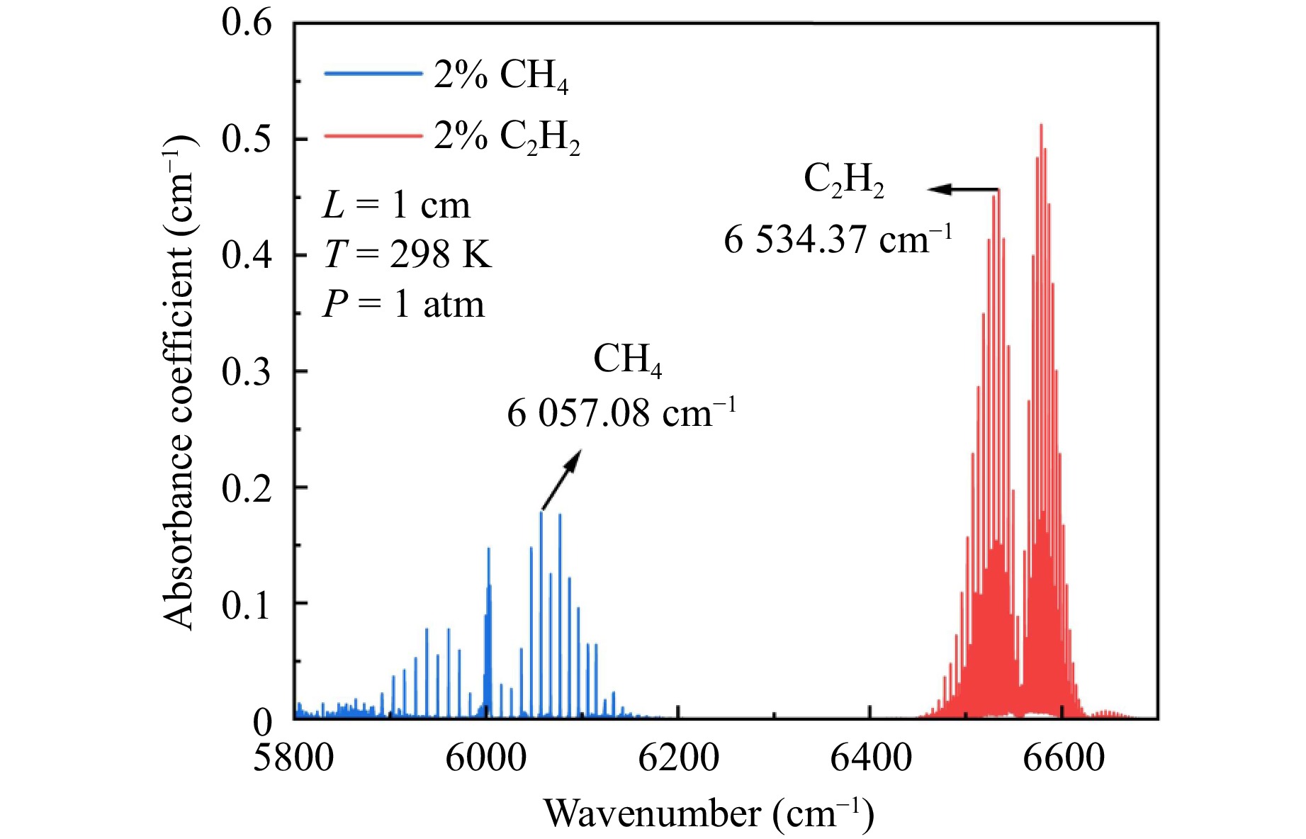
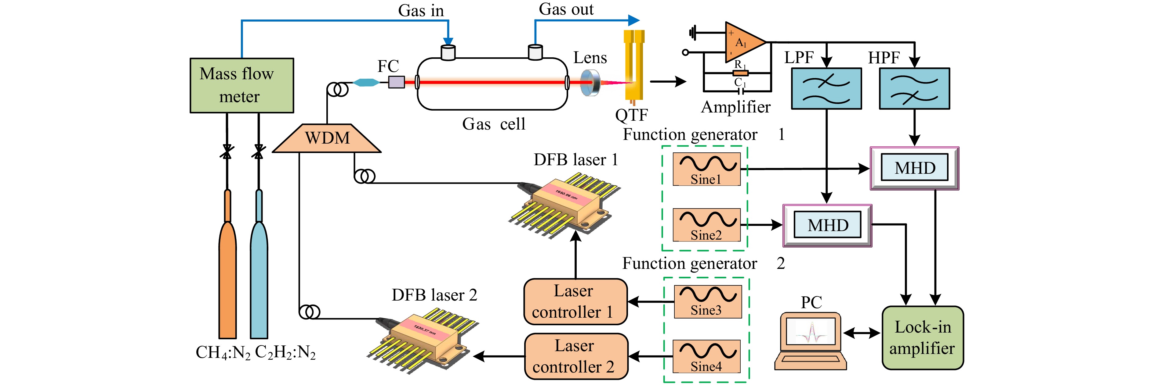
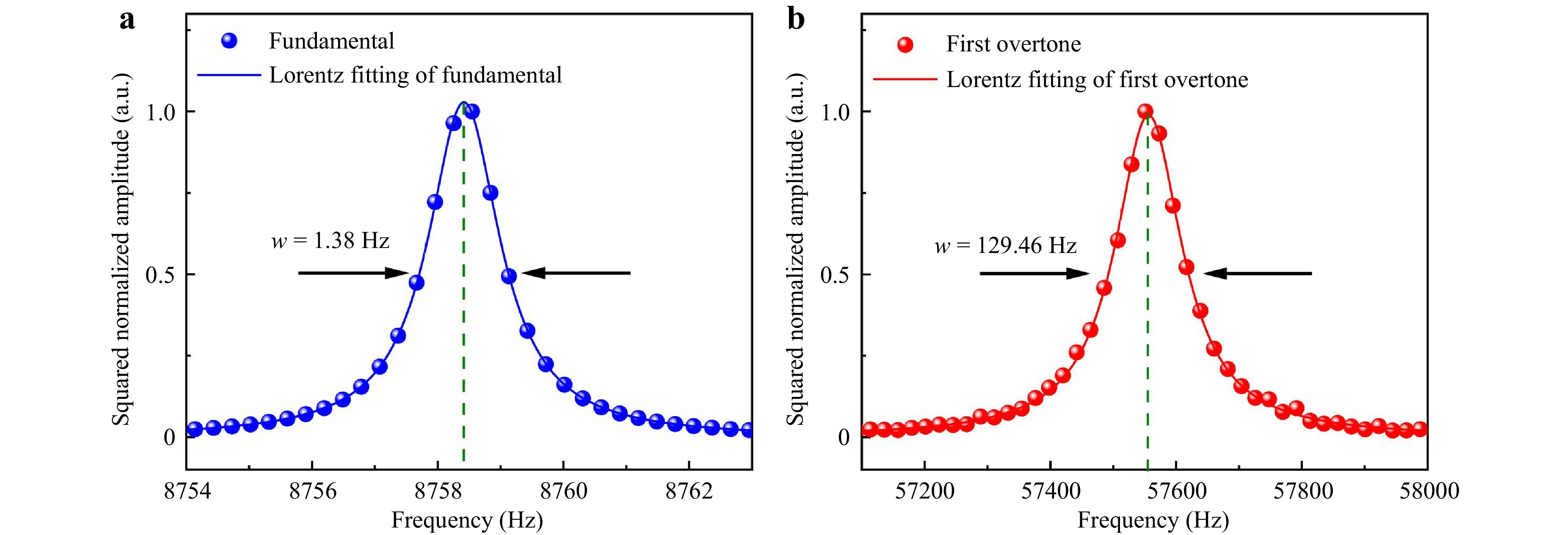
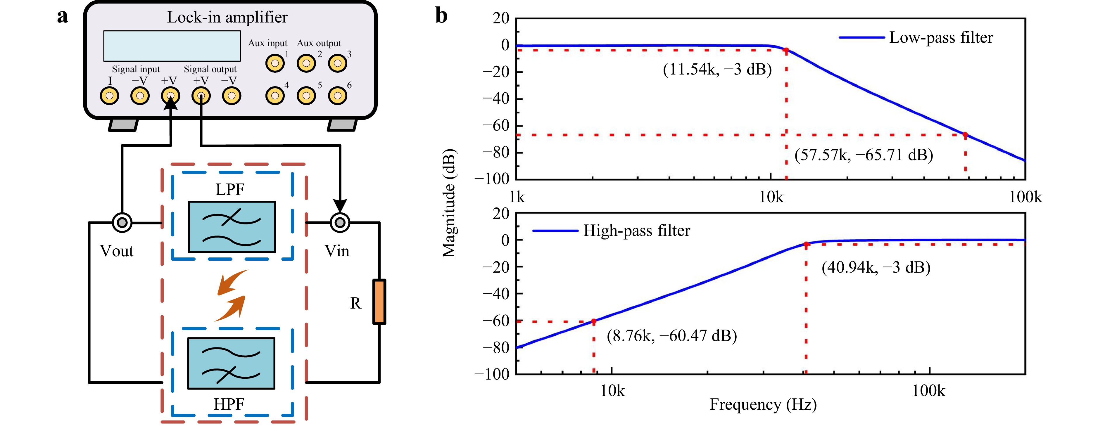
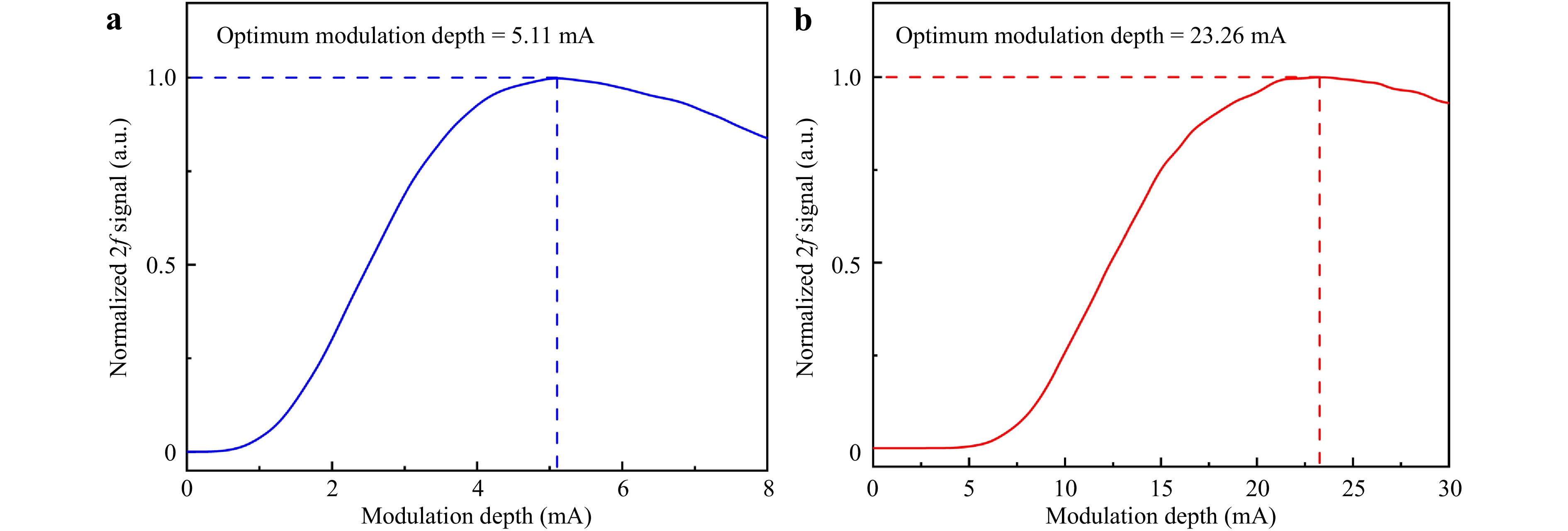
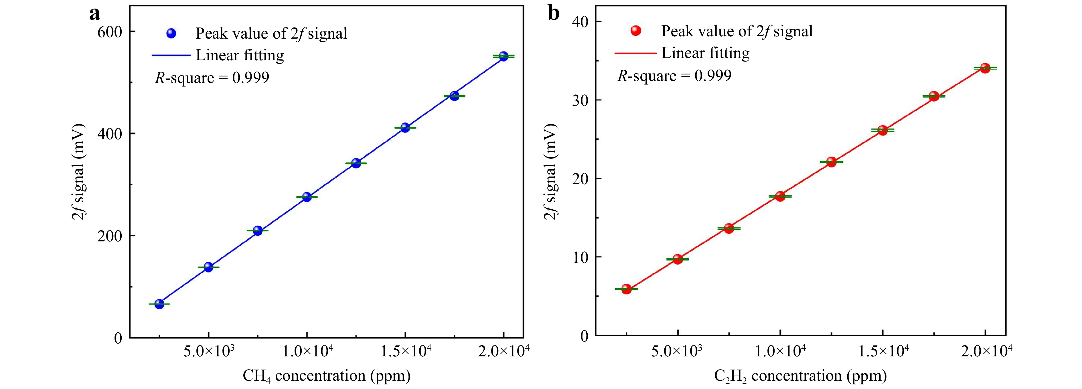
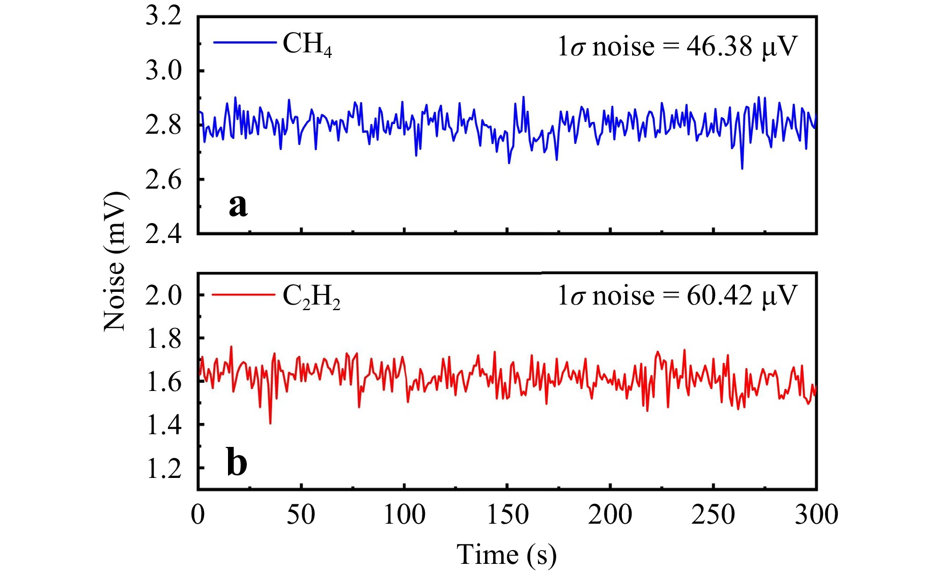
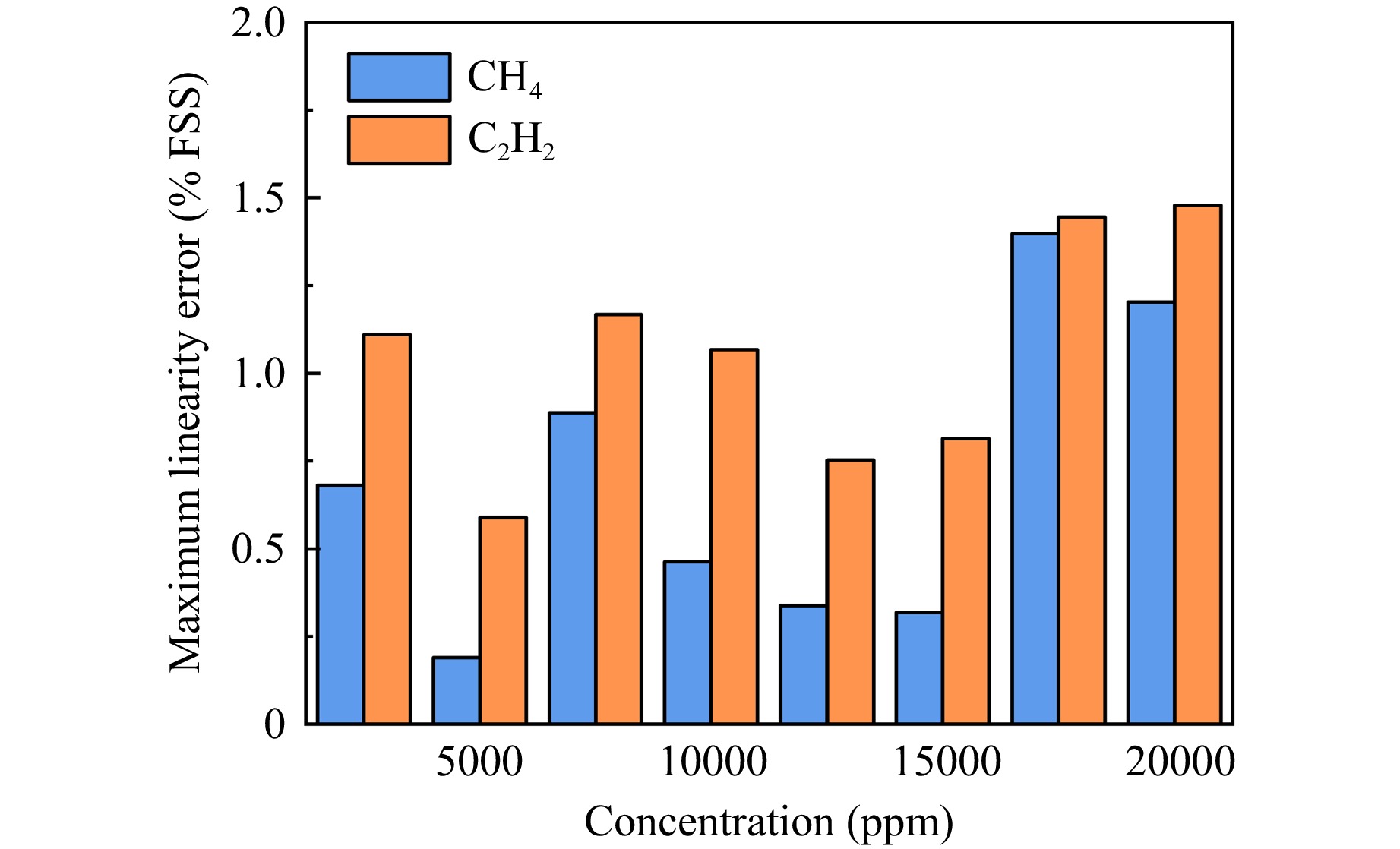
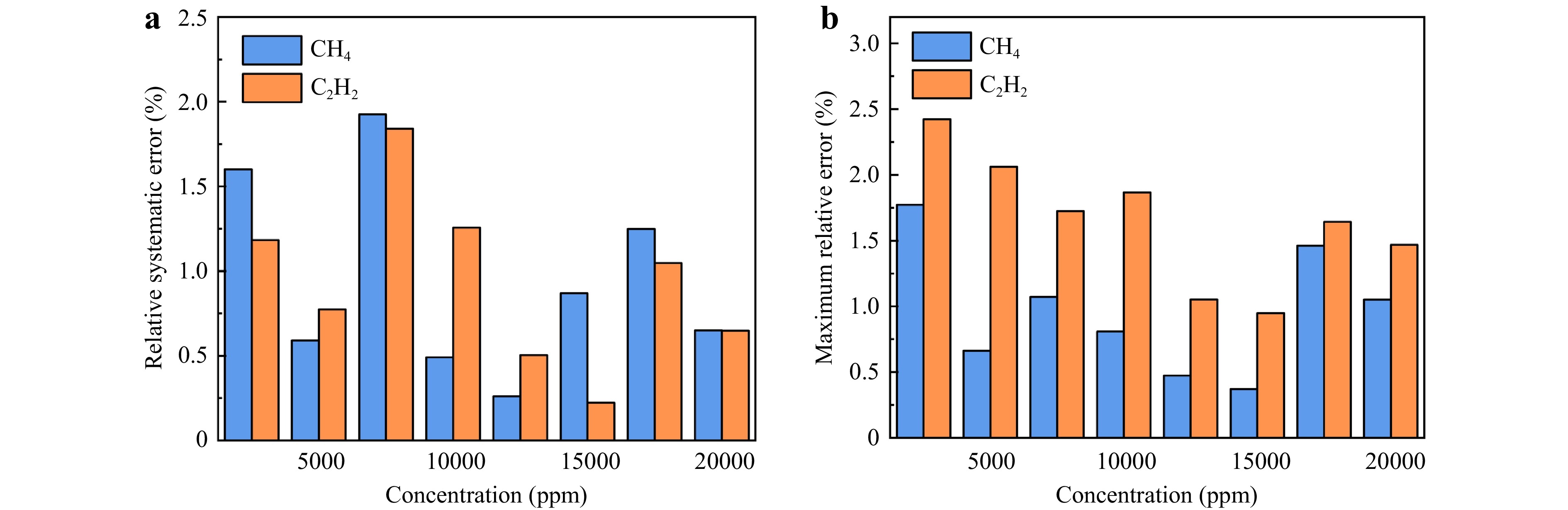
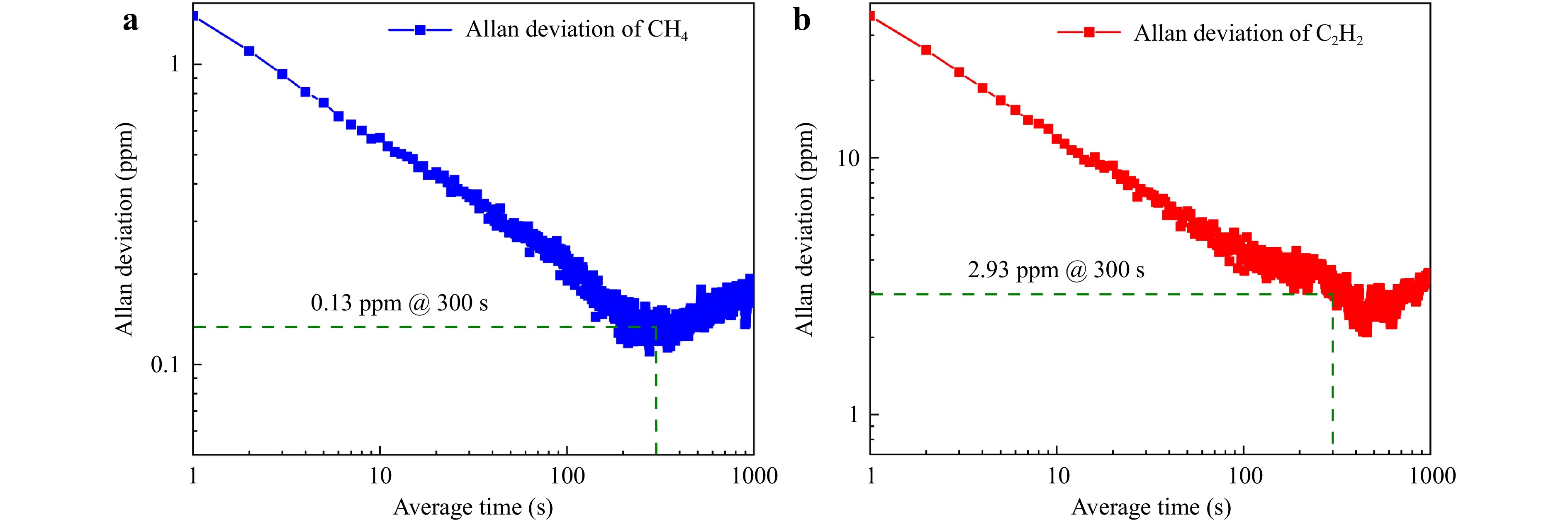
A novel dual-gas light-induced thermoelastic spectroscopy (DG-LITES) sensor based on mixed-frequency heterodyne demodulation (MHD) is reported. The DG-LITES sensor exploits the fundamental and first overtone vibration modes of a single self-designed low-frequency quartz tuning fork to achieve the high-performance simultaneous detection of methane (CH4) and acetylene (C2H2). Using a frequency-division multiplexing mechanism, this technique creates dual detection channels based on a single sensing element. Furthermore, it uses the MHD method to convert photothermal signals at different frequencies into a unified intermediate frequency, thereby enabling synchronous demodulation with only one correlation demodulation unit. The DG-LITES sensor not only maintains system compactness but also effectively suppresses inter-channel crosstalk below 0.057%. Experimental results demonstrated that the DG-LITES sensor exhibited excellent linear responses to both CH4 and C2H2 (R2 > 0.999), with maximum nonlinearity errors as low as 1.39% and 1.48% full-scale span, respectively. The mean relative systematic errors were 0.95% and 0.93%, respectively, whereas the maximum relative errors were 1.8% and 2.5%, respectively. Allan deviation analysis validated the excellent long-term operational stability of both the CH4 and C2H2 channels. The minimum detection limits for both channels were 0.13 and 2.93 ppm, with normalised noise-equivalent absorption coefficients of 2.73 × 10⁻⁹ and 9.61 × 10⁻⁸ cm−1·W·Hz−1/2, respectively. This paper presents a universal sensing architecture that offers a novel solution to the long-standing trade-off between performance and system complexity in multi-gas detection.
Published. 2026, 7(3)
: 660-672
doi: 10.37188/lam.2026.042
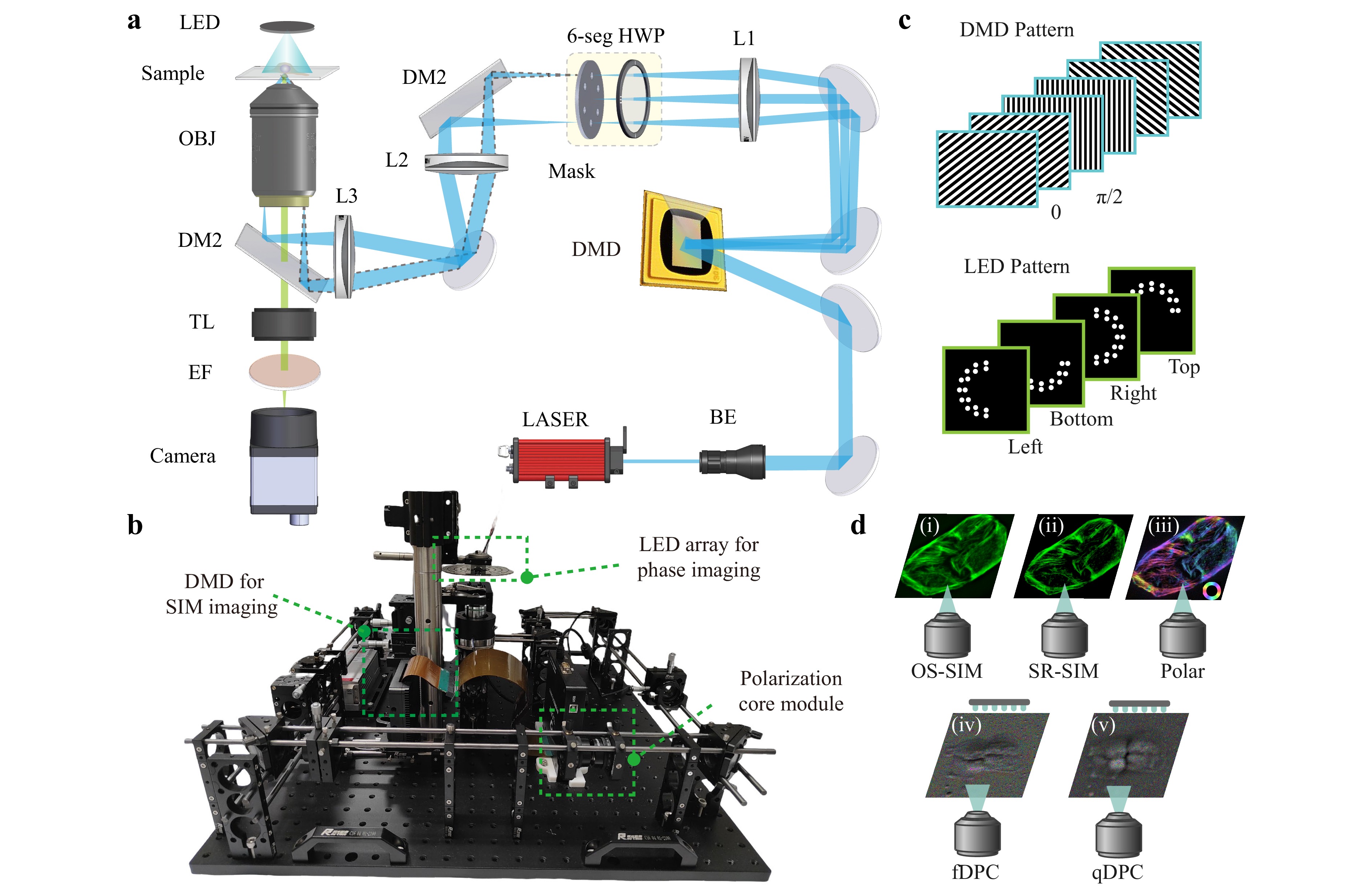
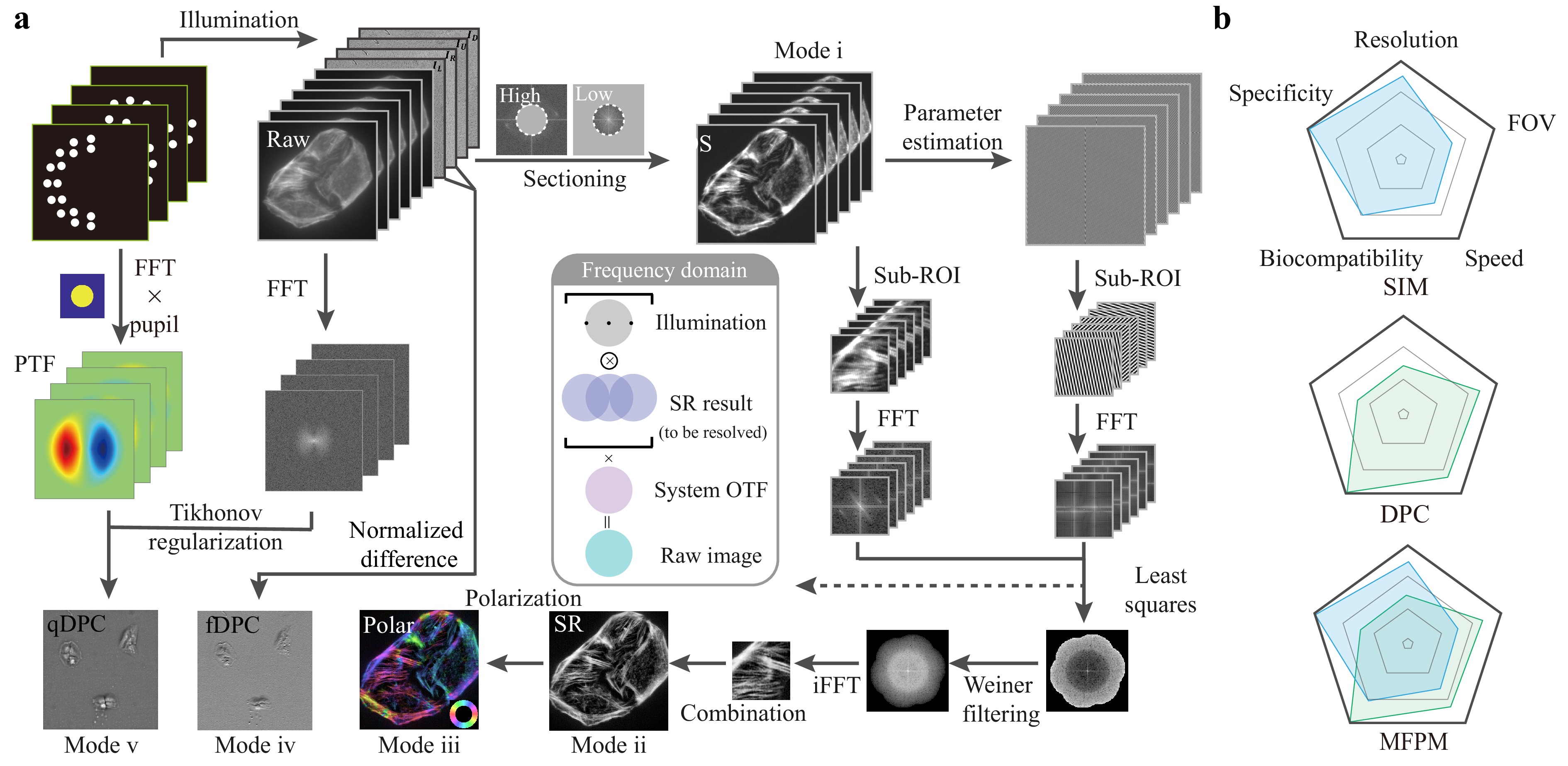
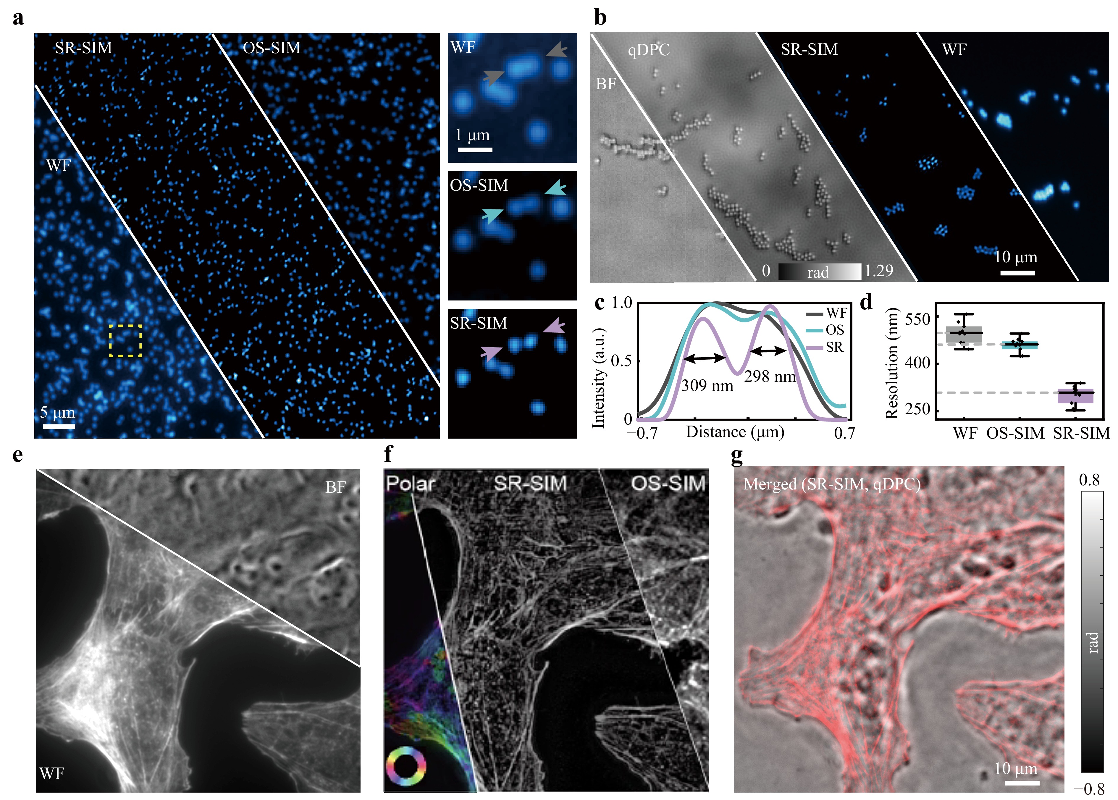
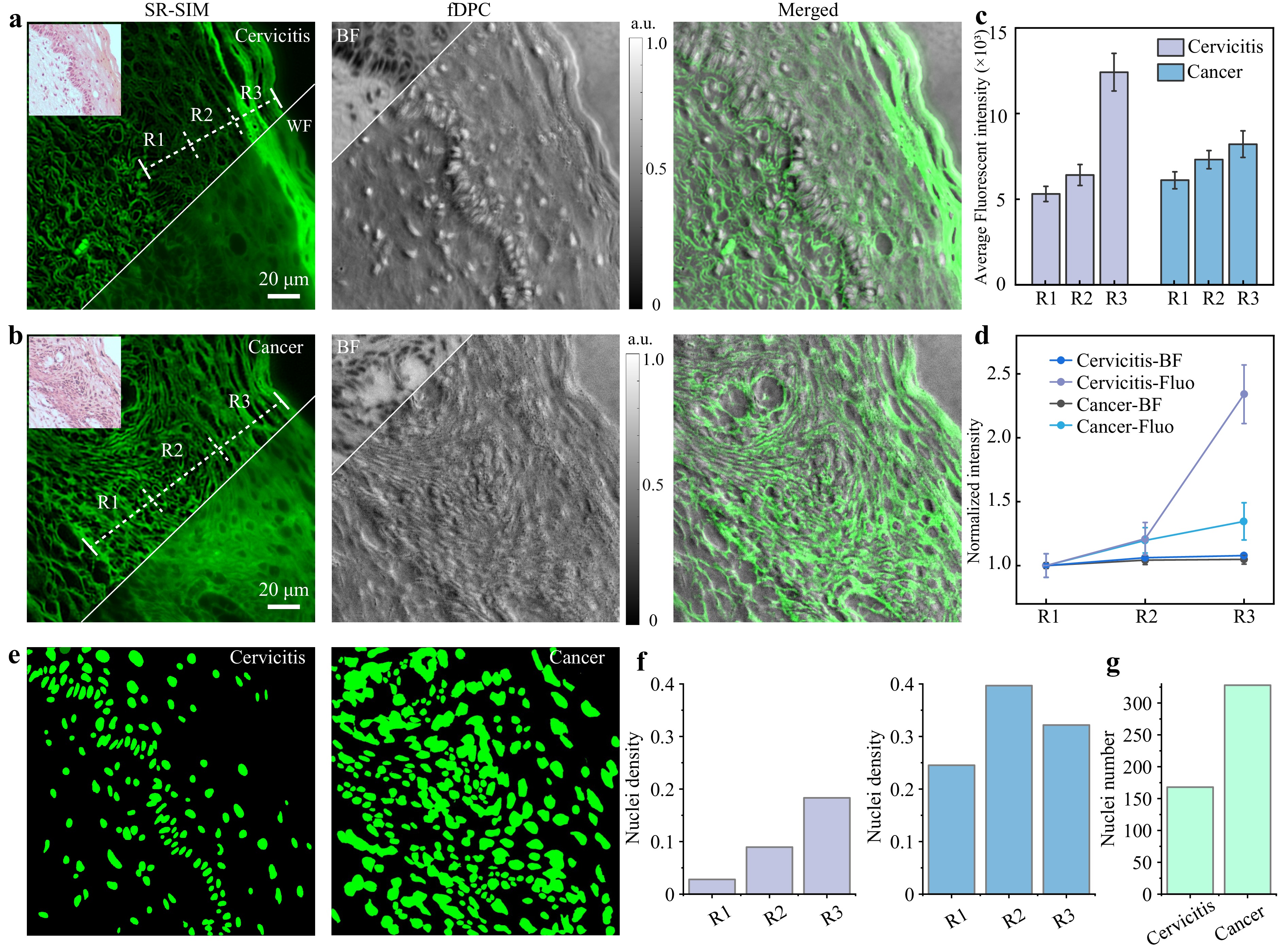
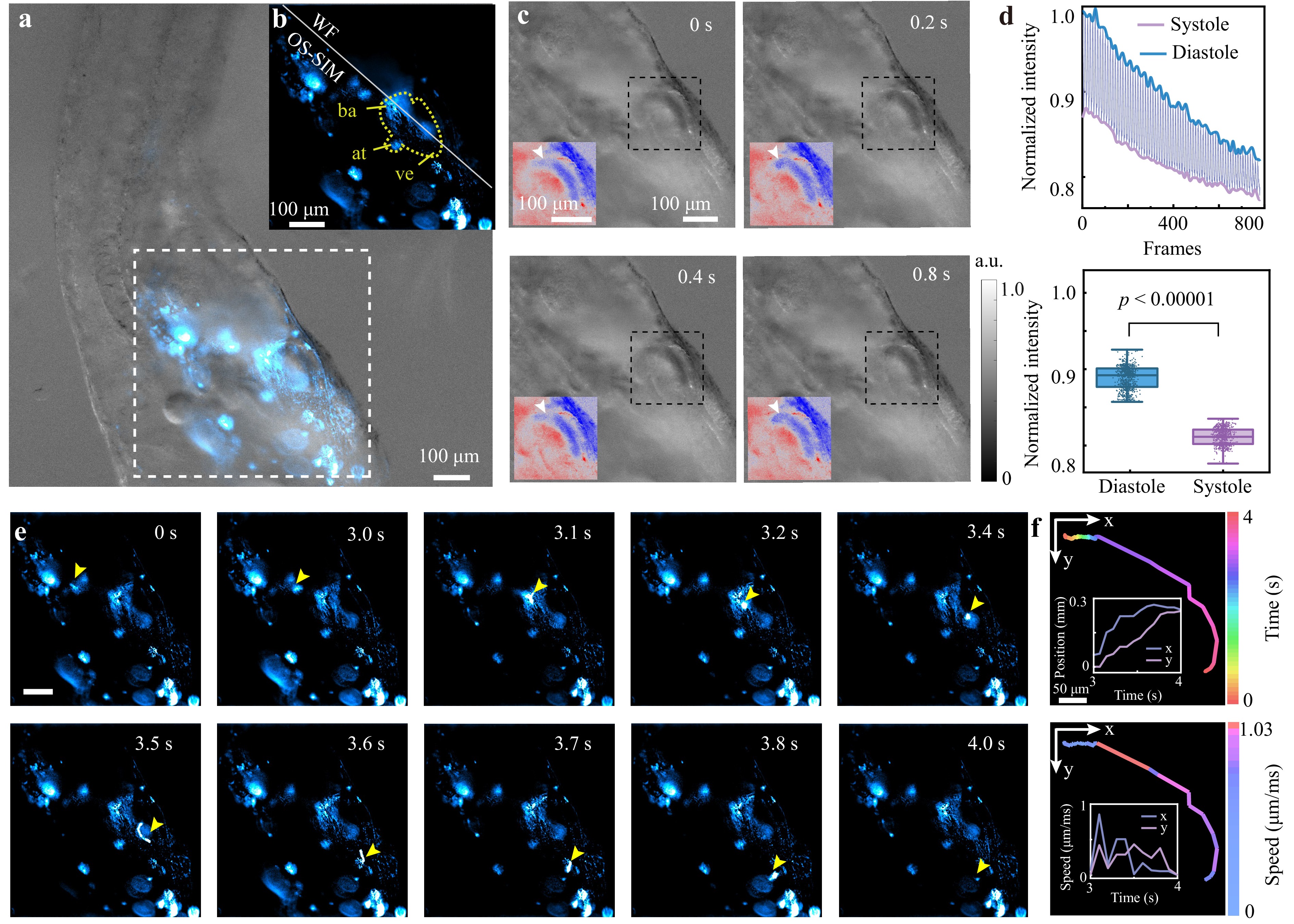
High-resolution, high-throughput, and minimally invasive imaging is in increasing demand in modern biomedical research. However, conventional single-modality optical microscopy often fails to satisfy these requirements. In this paper, we present a highly integrated multimodal fluorescence-phase microscopy (MFPM) system. By leveraging illumination pattern encoding, a unified wide-field detection configuration, and an integrated computational algorithm, MFPM achieves five imaging modes: optical-sectioning structured illumination microscopy (OS-SIM), super-resolution structured illumination microscopy (SR-SIM), polarisation dipole analysis, fast differential phase contrast (fDPC), and quantitative differential phase contrast (qDPC) imaging. By incorporating dark channel prior-based background removal, MFPM achieves improved imaging depth, whereas the frame-reduction strategy enables a higher imaging speed. Consequently, only ten raw frames are required to reconstruct multidimensional information. This integrated platform enables co-registered multimodal imaging for diverse biomedical applications, including the subcellular visualisation of U2OS cells, quantitative auxiliary diagnosis of pathological tissue sections, and analysis of zebrafish heartbeats. With its compact design and multidimensional imaging capabilities, MFPM offers a unified solution for structural and functional imaging. Its scalability toward intelligent event-triggered imaging, and virtual staining integration makes it a promising platform for next-generation automated biomedical imaging.
Published. 2026, 7(3)
: 673-688
doi: 10.37188/lam.2026.046
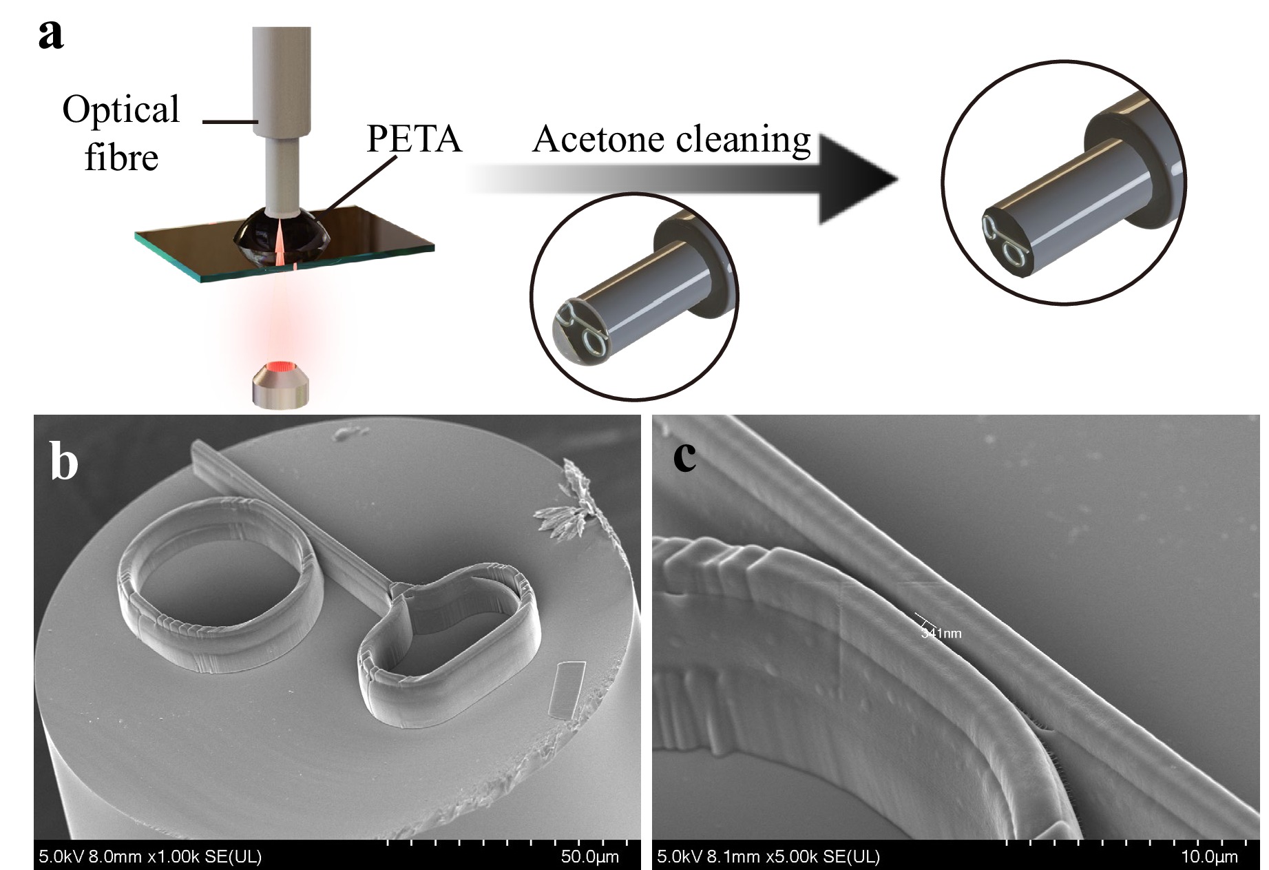
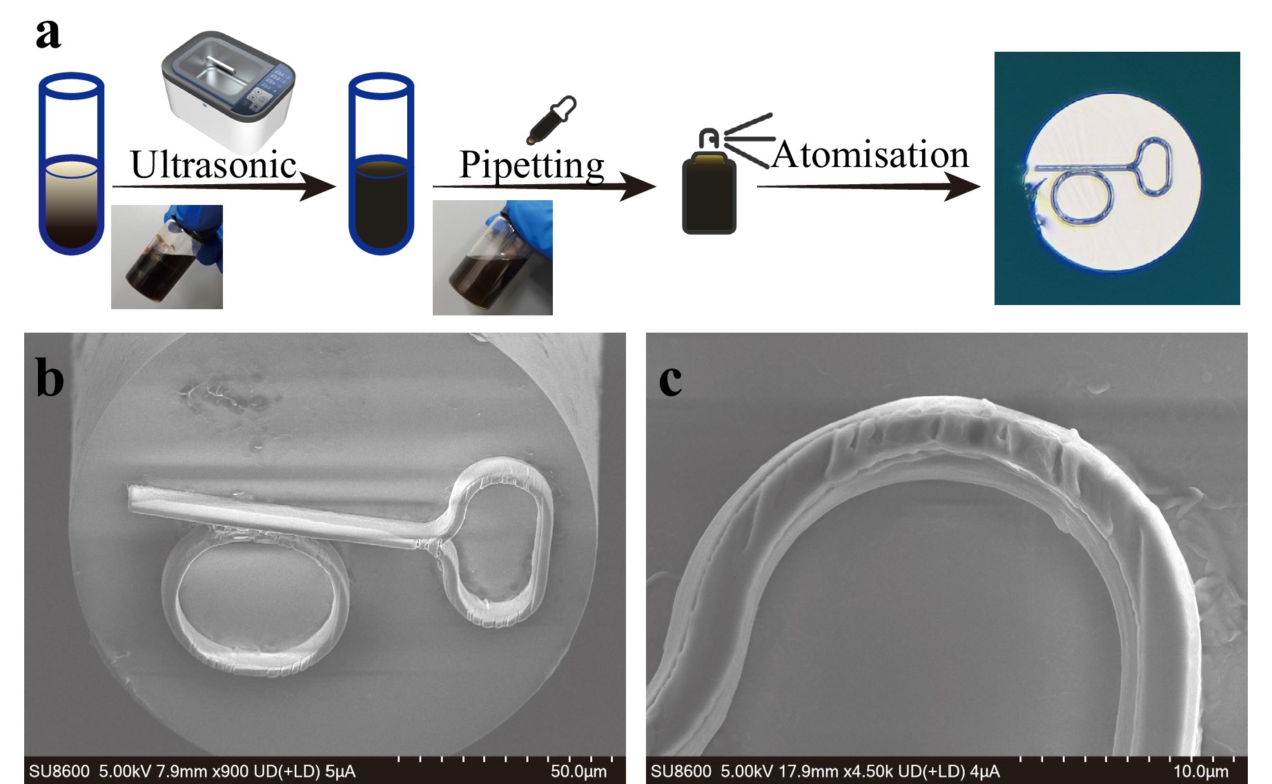
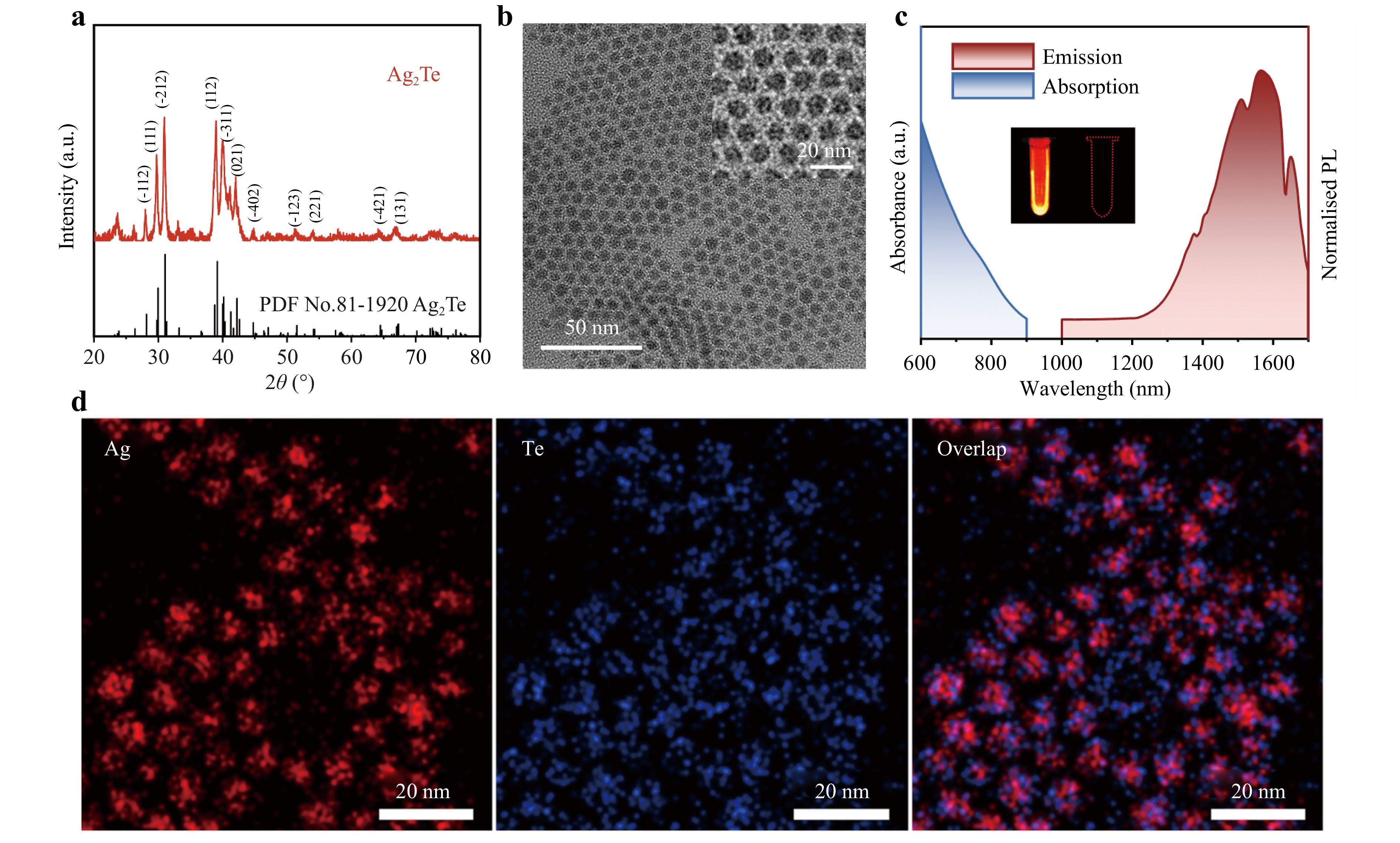
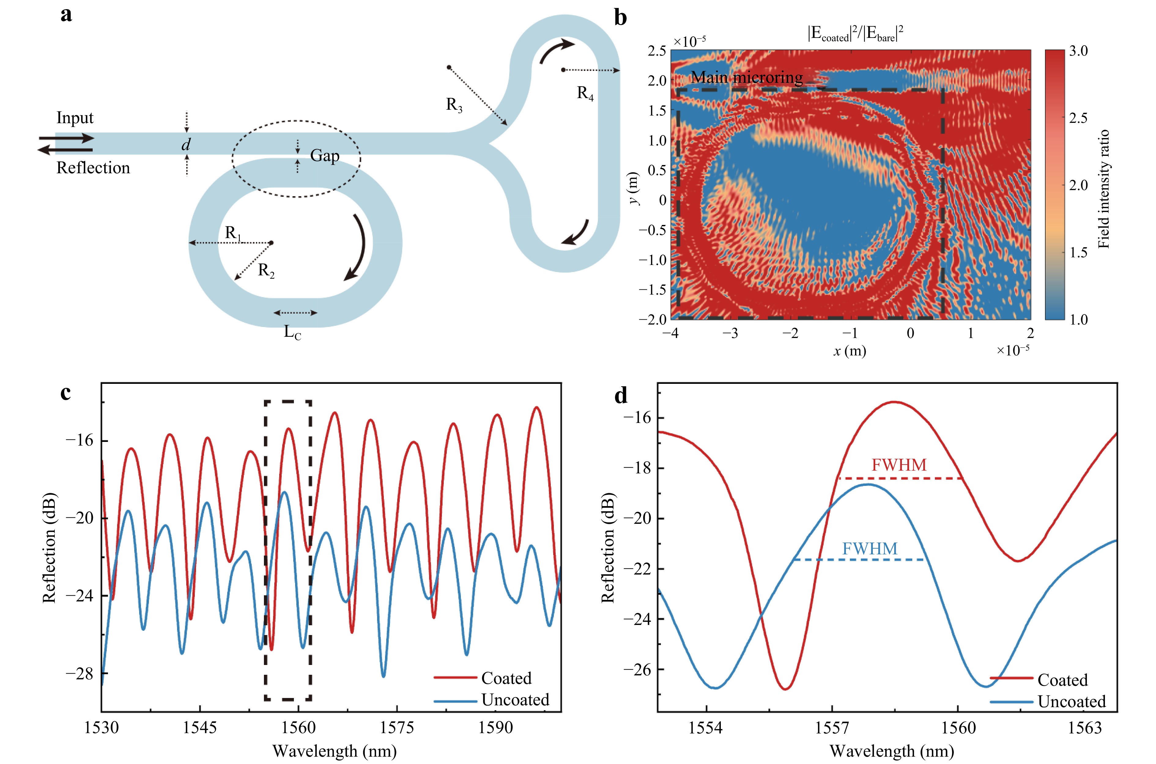
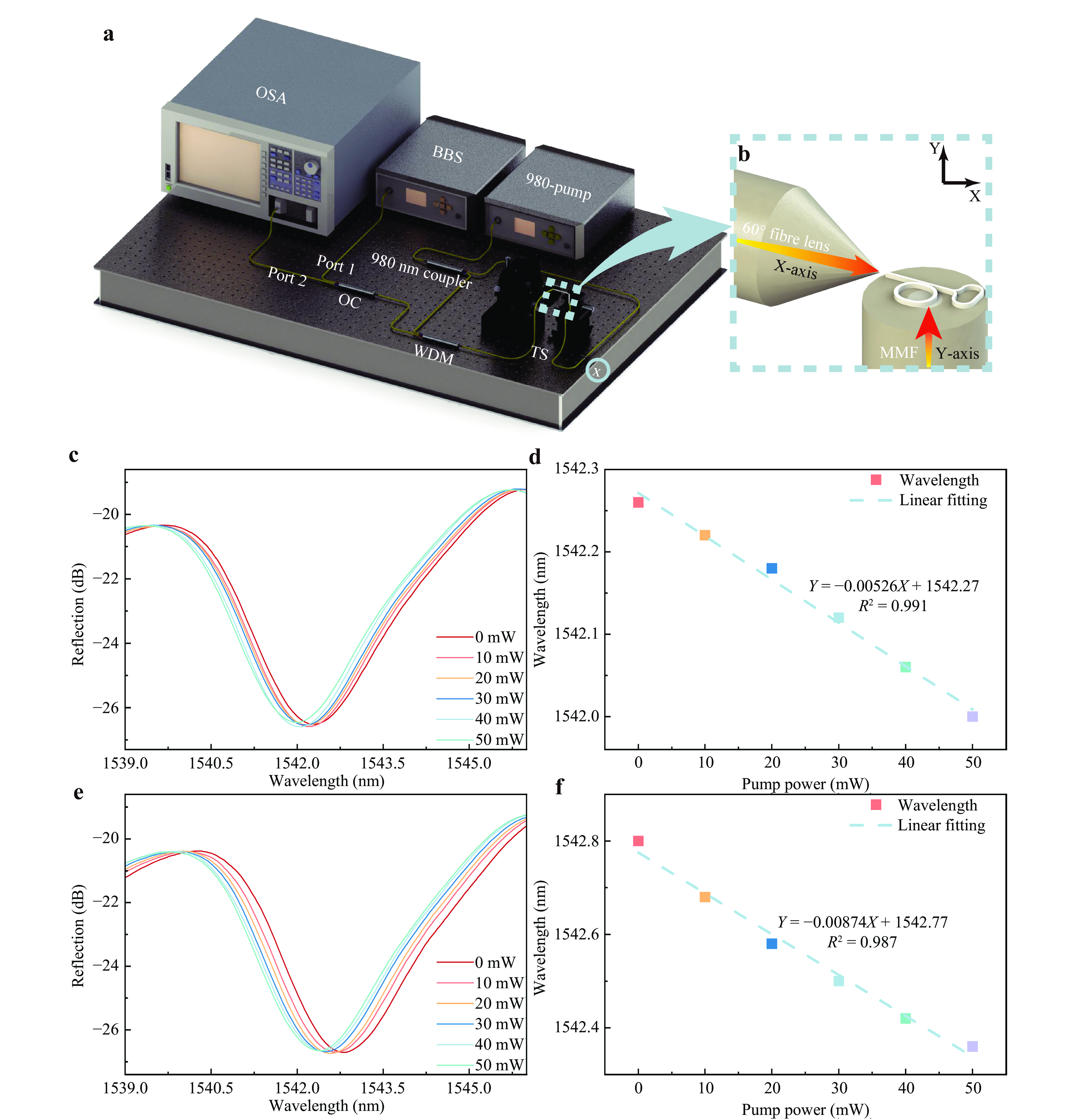
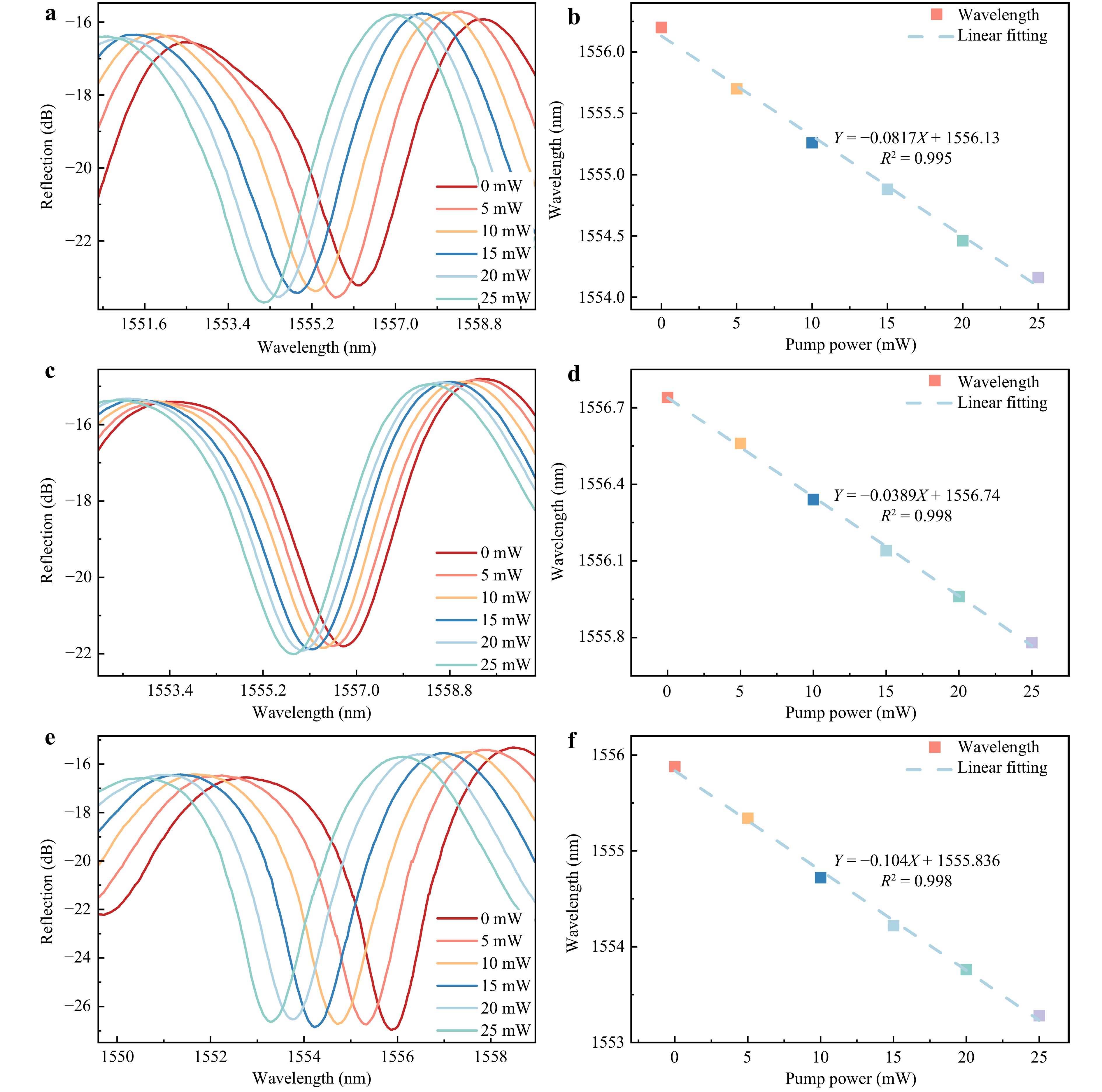
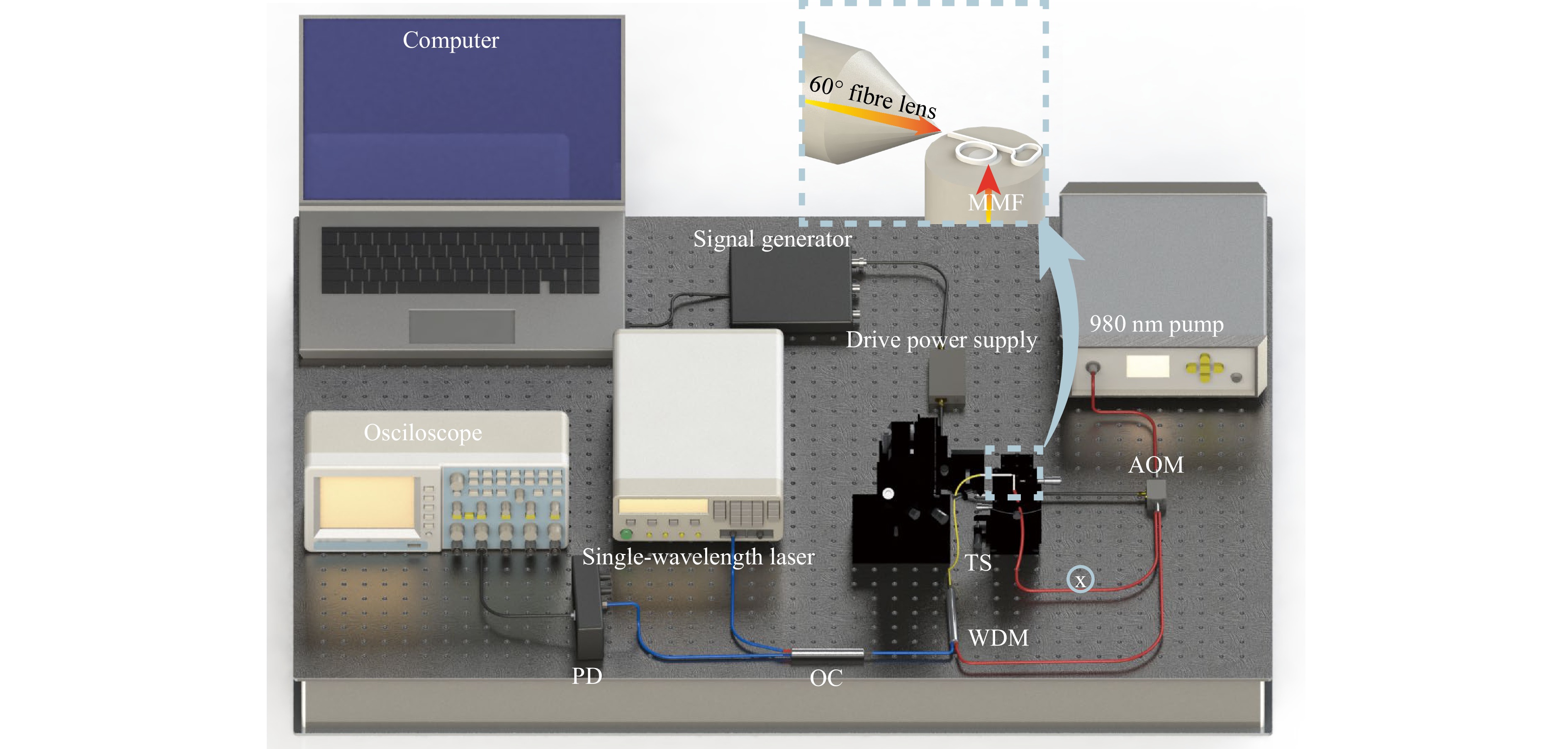
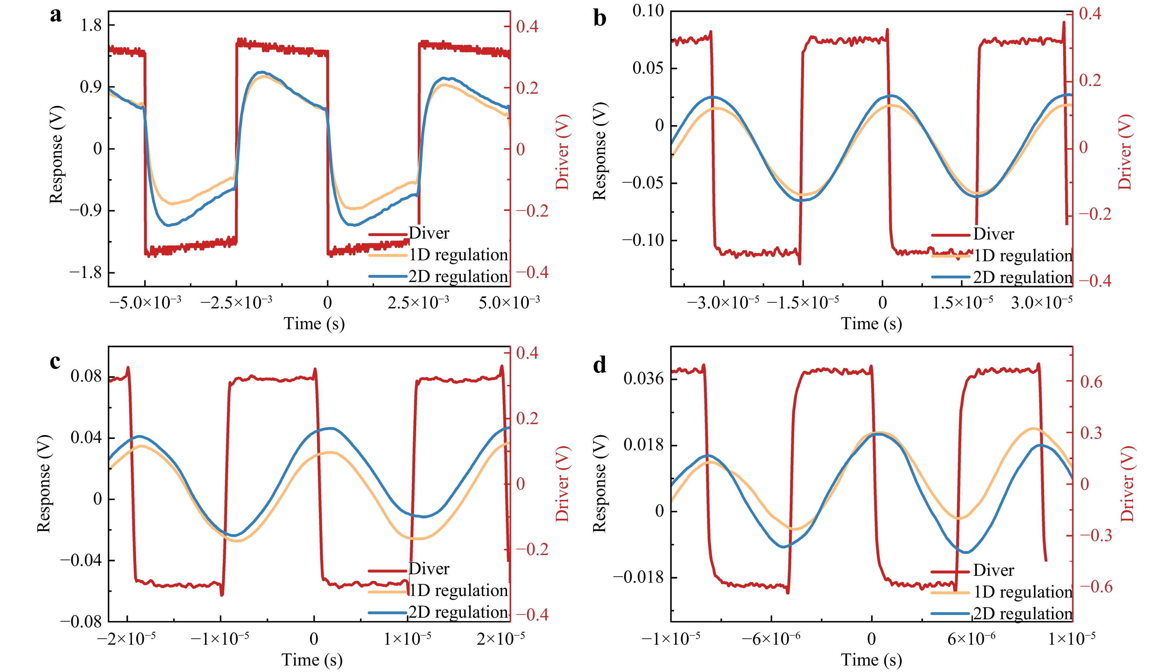
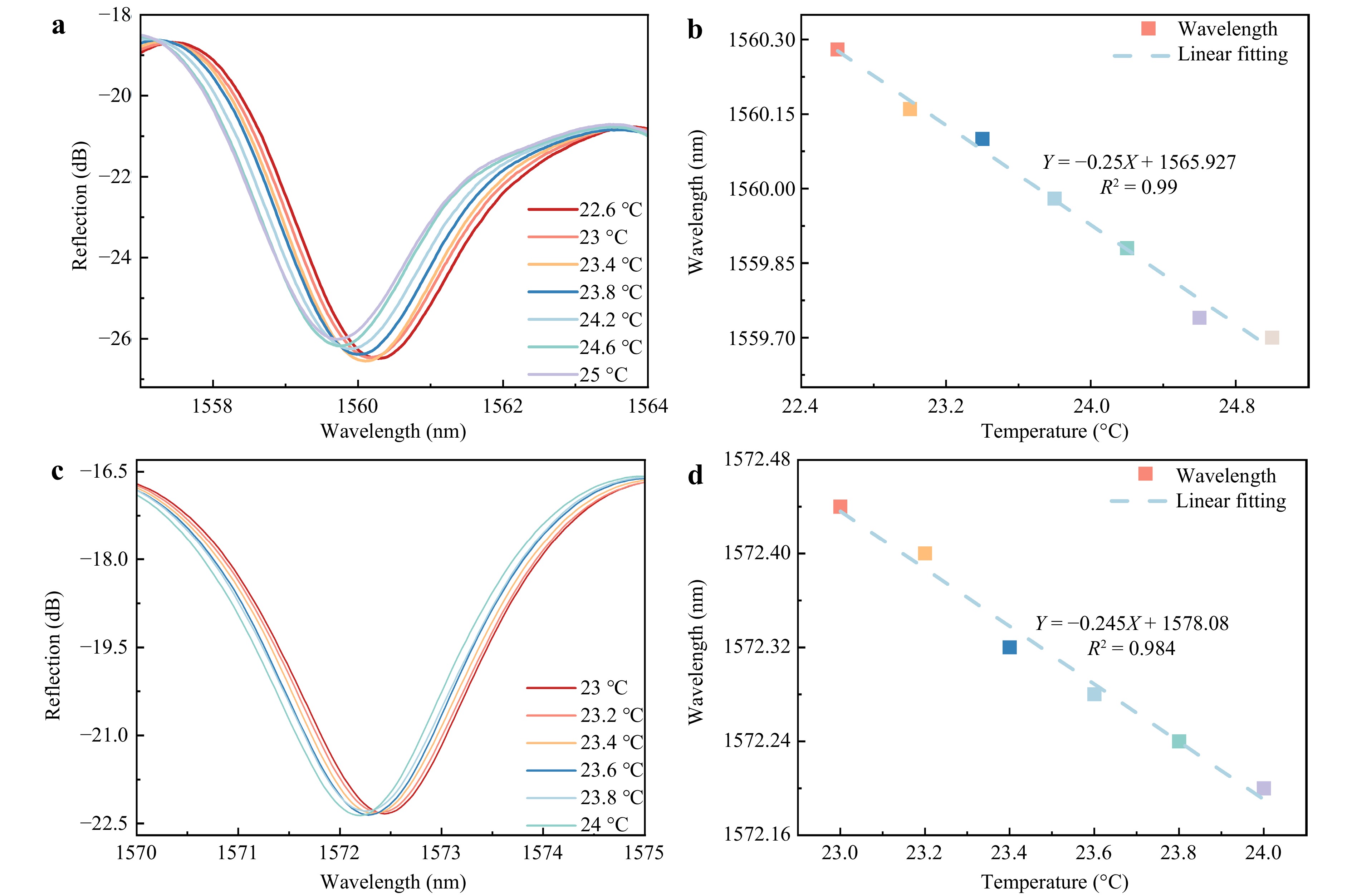
Beyond conventional thermo-optic (TO) devices, this study introduces a hybrid photonic platform integrating a polymer micro-ring resonator (MRR), fabricated via two-photon printing and functionalized with Ag2Te quantum dots (QDs), onto a fibre end. By leveraging advanced two-photon micro-printing, we precisely fabricated complex hybrid MRR structures, thereby facilitating unprecedented on-chip integration and intricate three-dimensional geometries that remain unattainable using traditional methods. The proposed platform utilises an Ag2Te QD-functionalized polymer film, wherein controlled interfacial engineering in conjunction with the intrinsic localised surface plasmon resonance (LSPR) of the QDs amplifies the local optical field by 300% and fundamentally reconfigures photon–thermal–carrier interactions. An innovative two-dimensional (2D) synergistic all-optical modulation strategy is employed, leading to substantial performance improvements, including a 19.77-fold enhancement in tuning sensitivity over standard polymer MRRs and 50-fold improvement in modulation speed, reaching up to 100 kHz, which significantly exceeds those of conventional TO platforms. This compact fibre-integrated architecture, enabled by precision additive manufacturing, delivers a robust, energy-efficient, and high-speed solution for dynamically reconfigurable on-chip TO modulation and represents a transformative step forward for integrated photonic circuits.
Published. 2026, 7(3)
: 689-699
doi: 10.37188/lam.2026.067
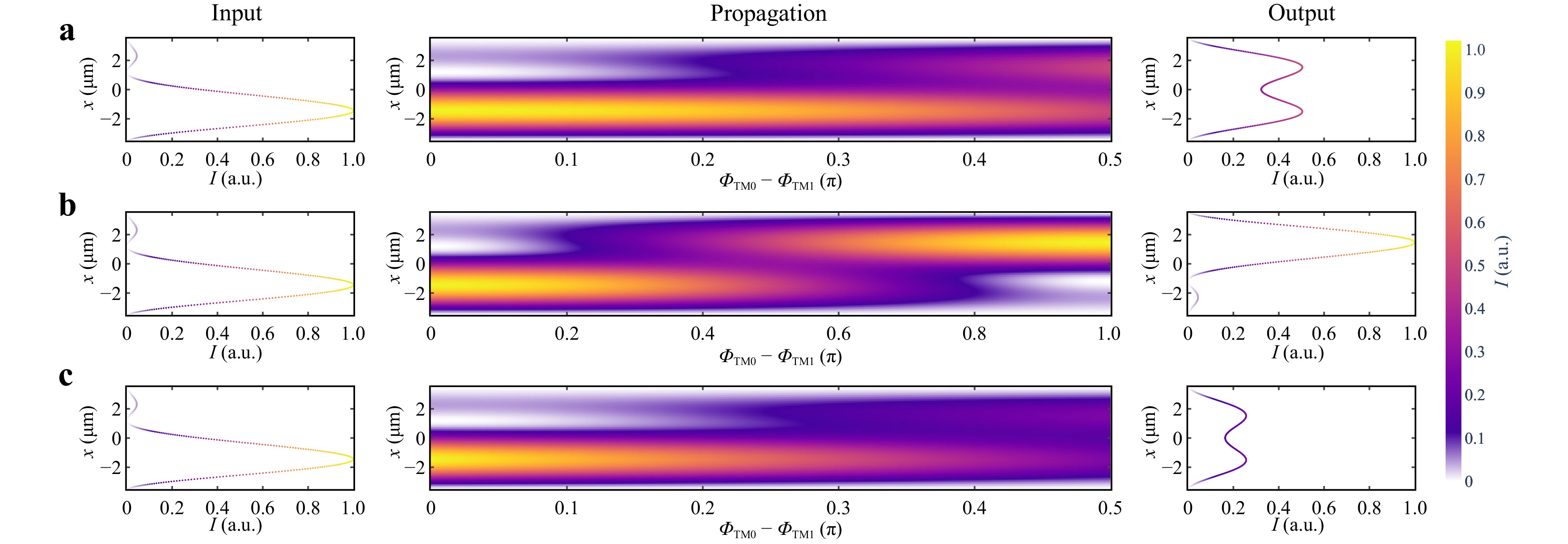
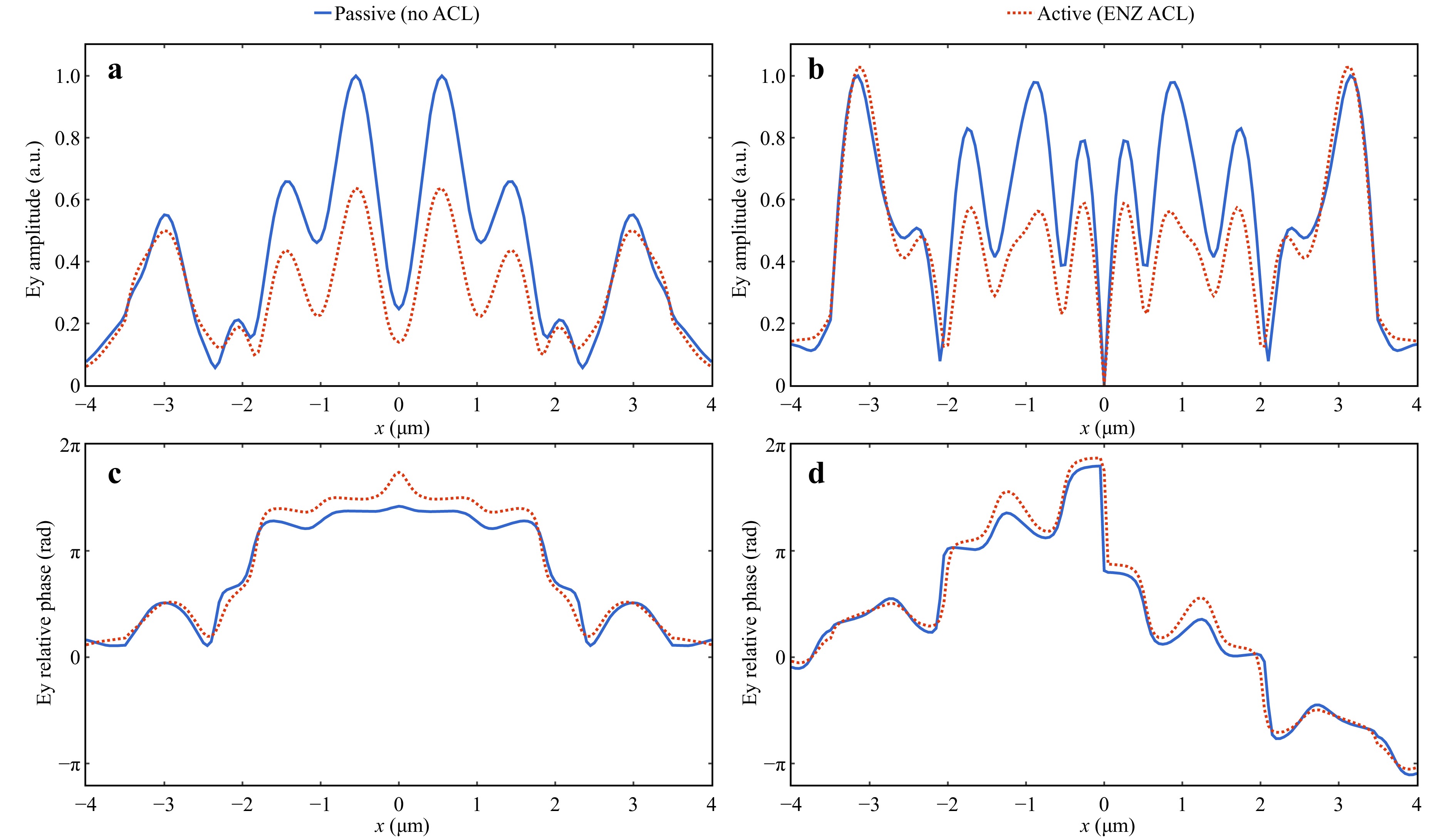
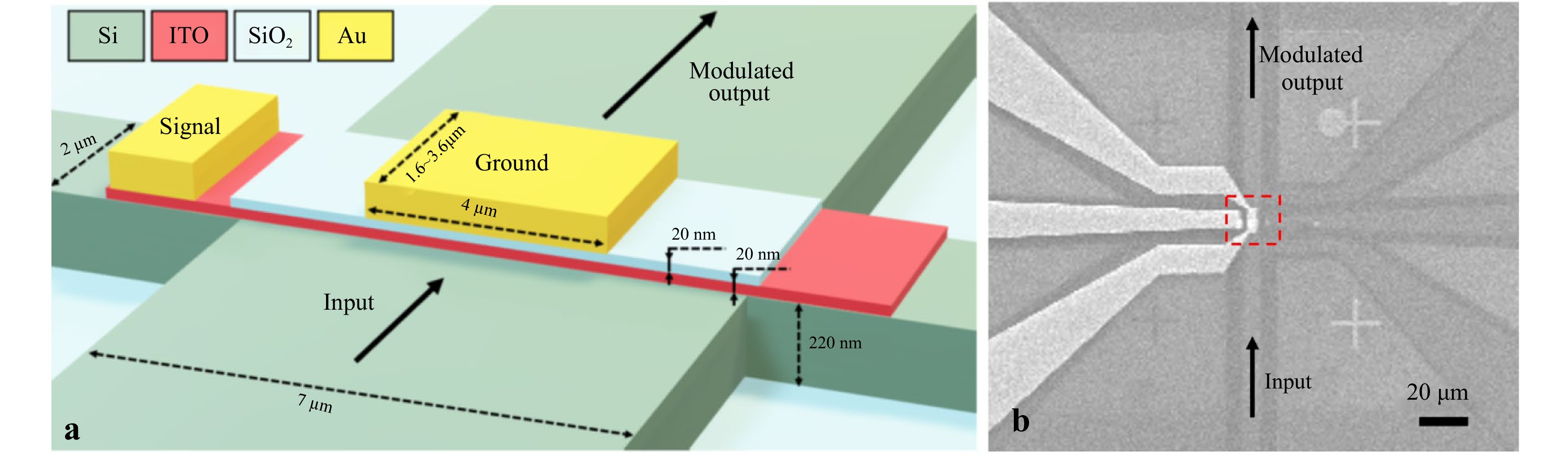
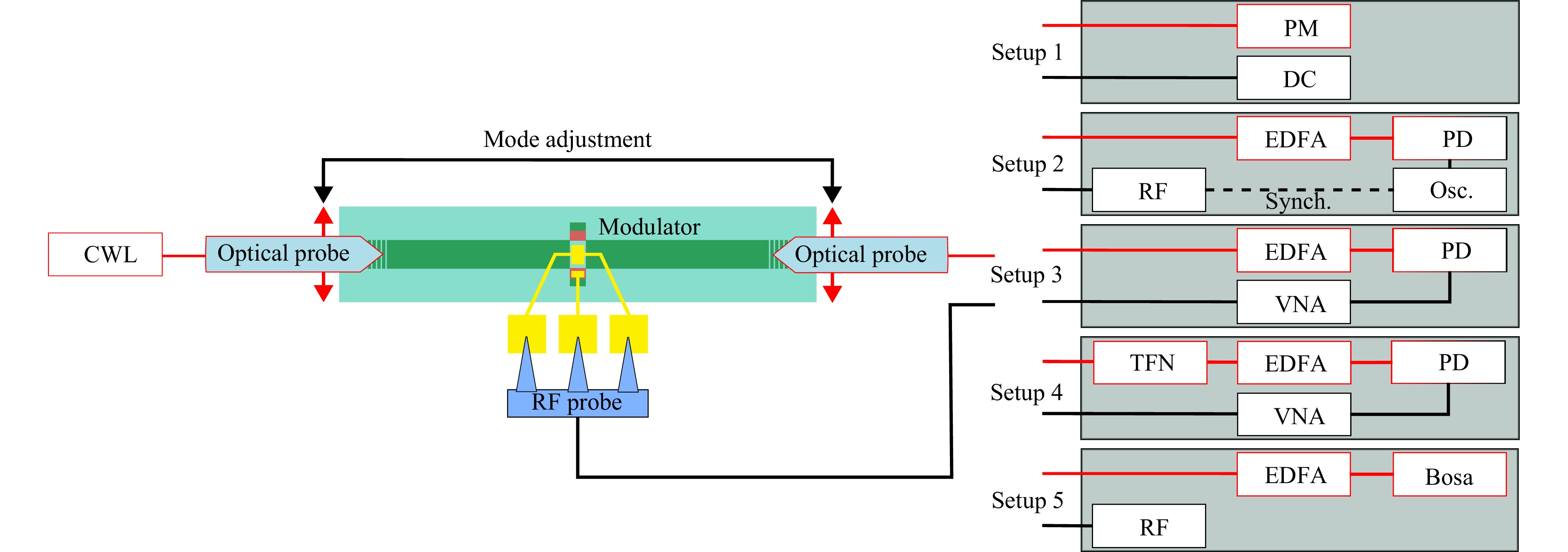
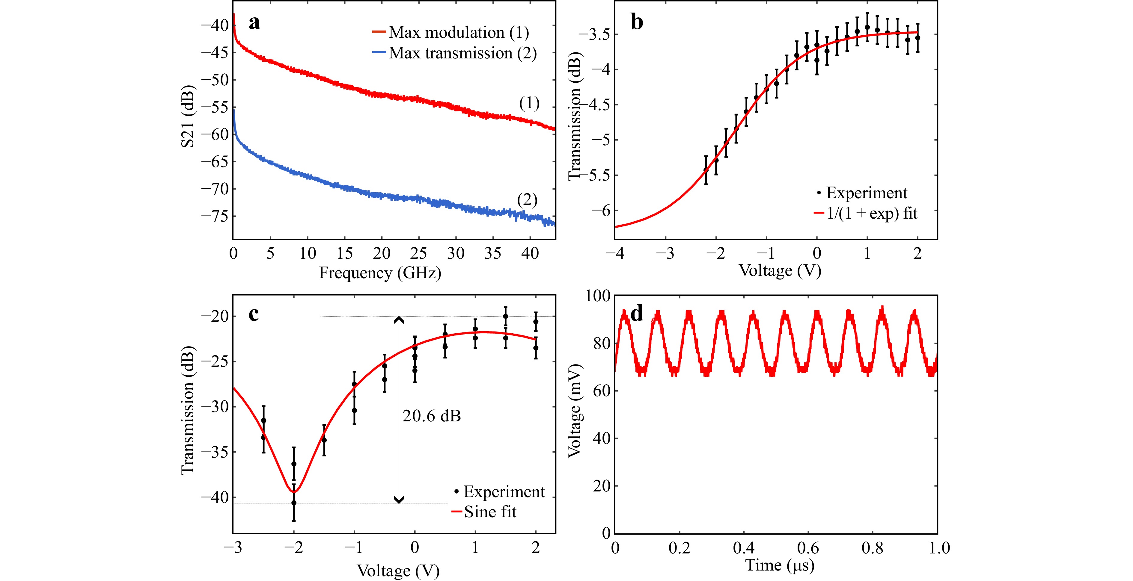
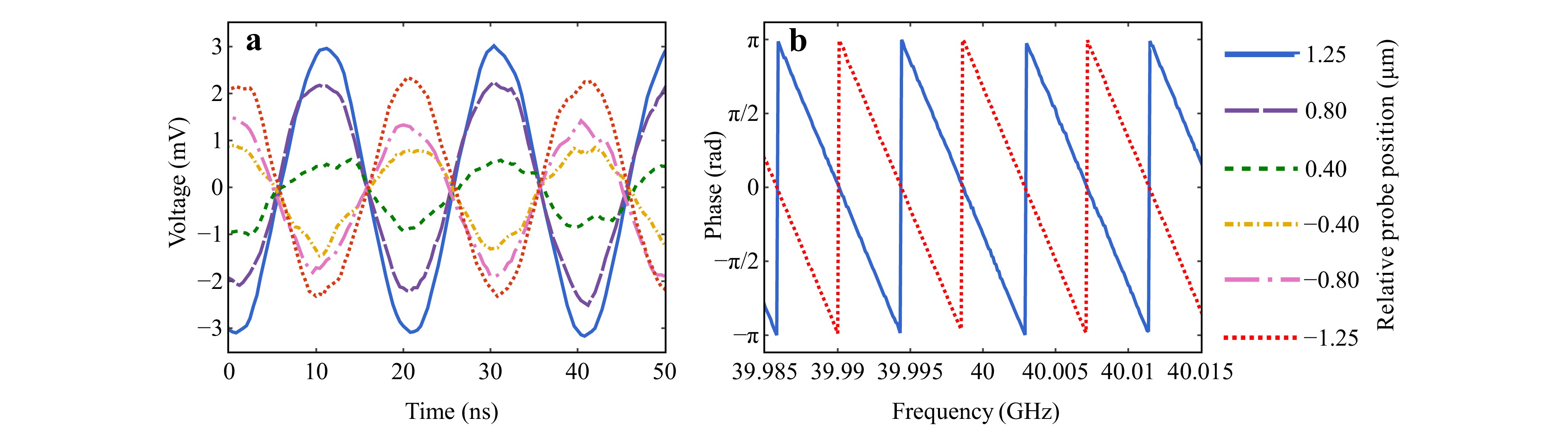
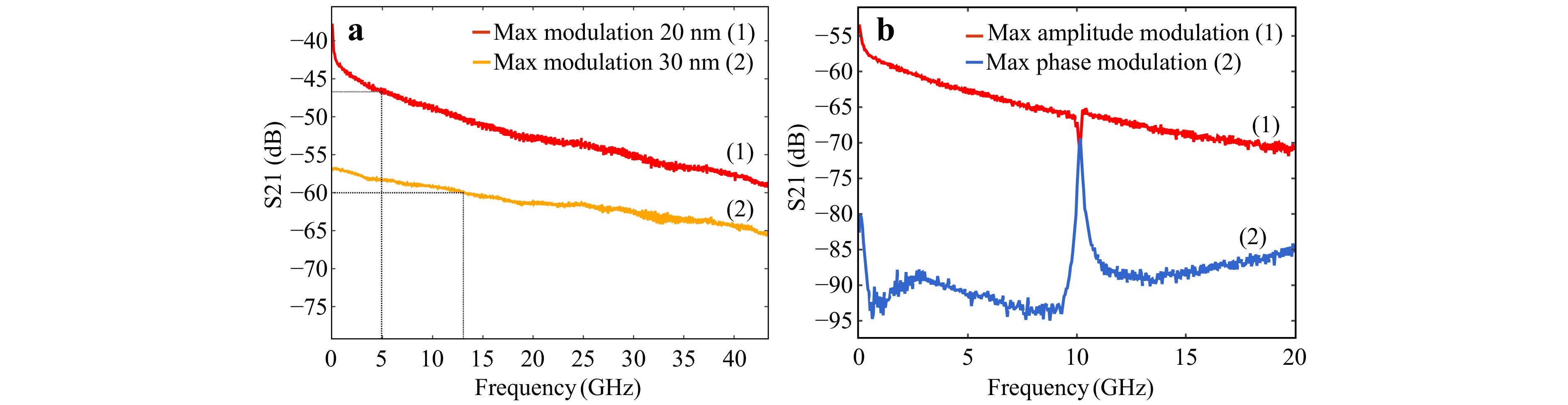
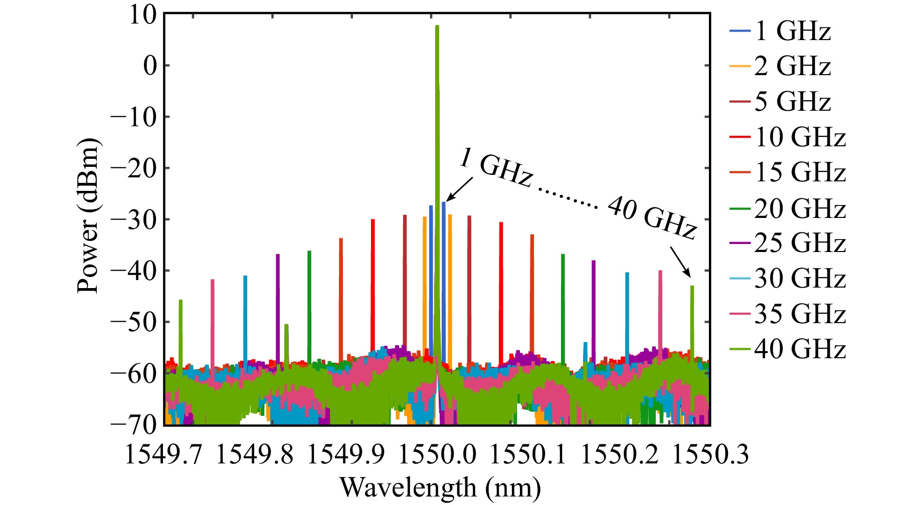
An ultra-compact silicon photonic solution based on a multimode plasmonic modulator is proposed for signal processing with complementary routing. The Si-ITO-SiO2-Au structure investigated in this study reveals previously unexplored mechanisms for signal management. In this modulator, both intensity and phase modulation can be selectively achieved. By controlling mode excitation, electro-refraction can be effectively converted into variations in multimode interference. As a result, a single-output grating coupler exhibits two spatially separated regions with inverted intensity modulation. Moreover, the modulation depth at these locations can be readily tuned. The measured DC extinction ratio over a voltage range of −2 to 1.5 V reaches 20.6 dB for a 1.6 µm-long modulator, corresponding to a record-high value of 12.8 dB/µm. The directly measured AC extinction ratio is 2.48 dB at a modulation frequency of 10 MHz, decreasing to 1.25 dB at 1 GHz over a voltage range of −2 to 2 V for a 3.6 µm-long modulator. These results demonstrate a significant step towards the integration of compact, high-speed, and reconfigurable analogue optical links for advanced signal processing.
Published. 2026, 7(3)
: 700-711
doi: 10.37188/lam.2026.041
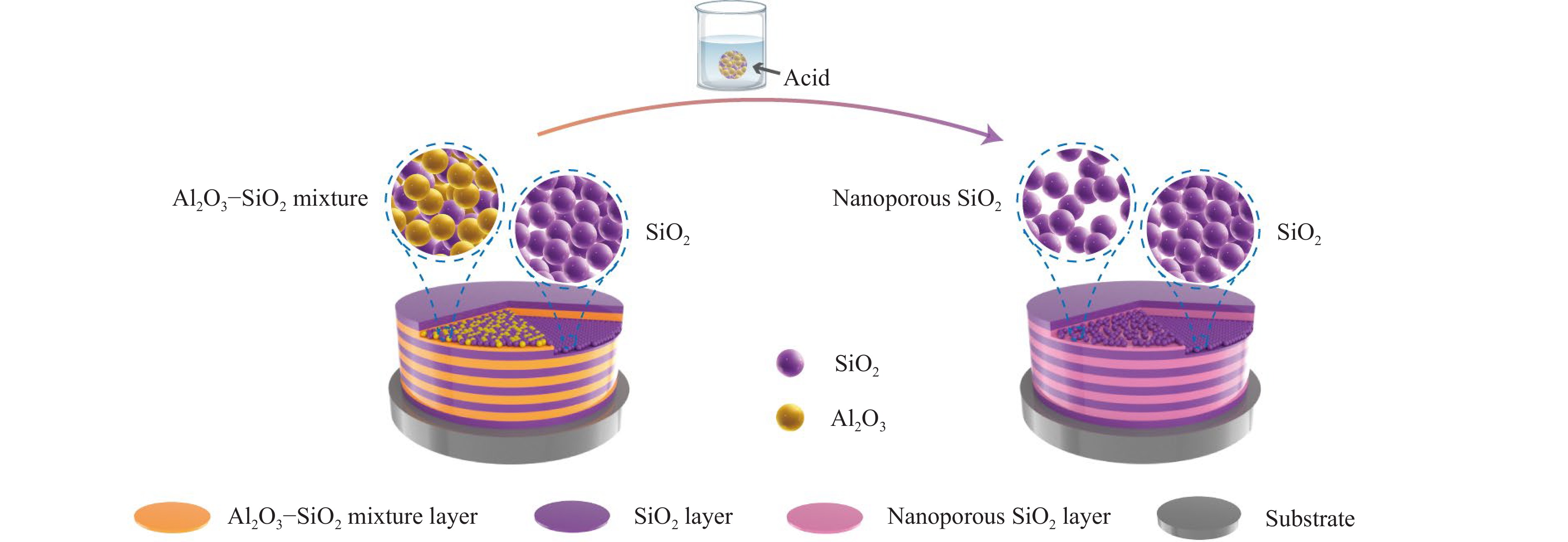
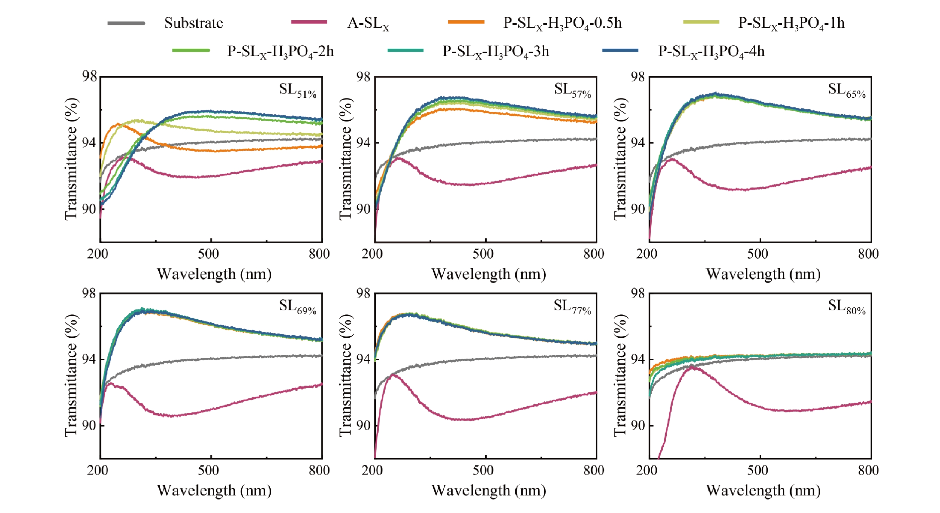
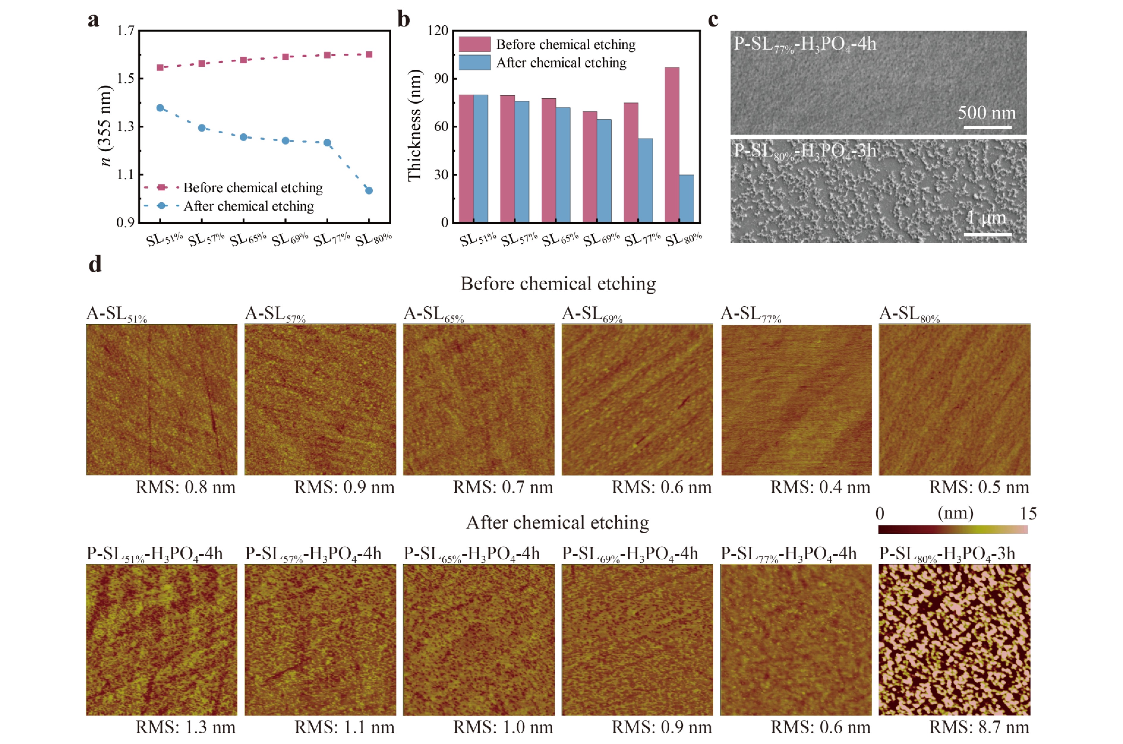
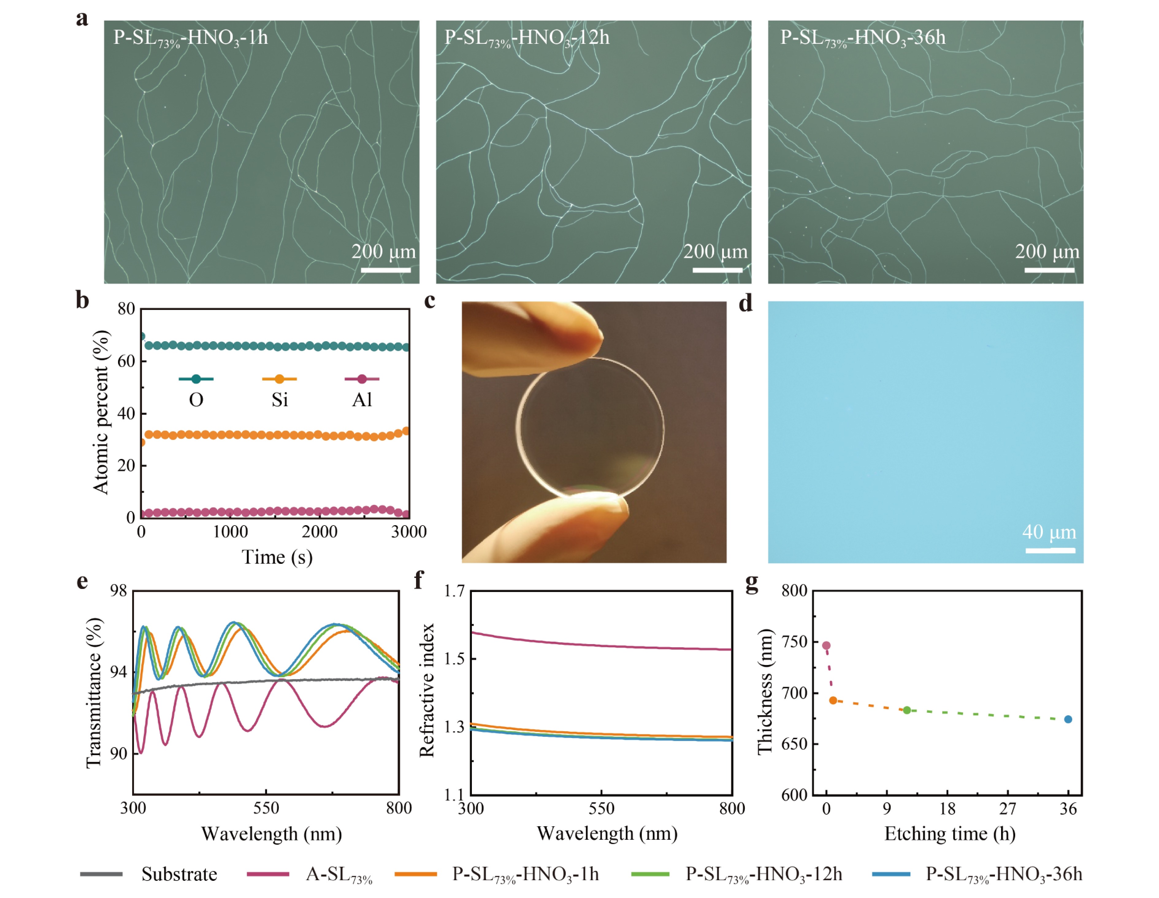
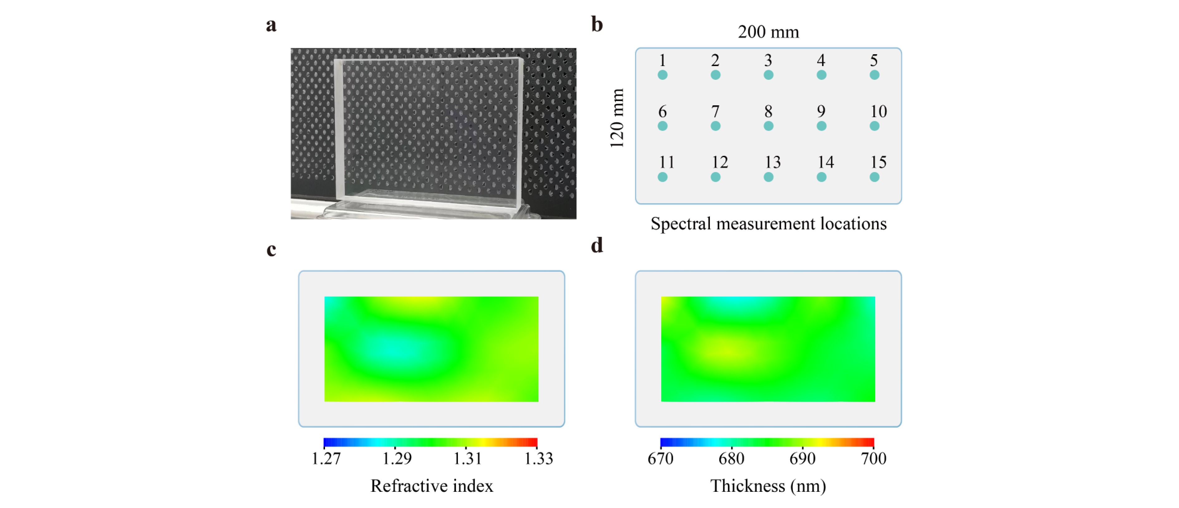
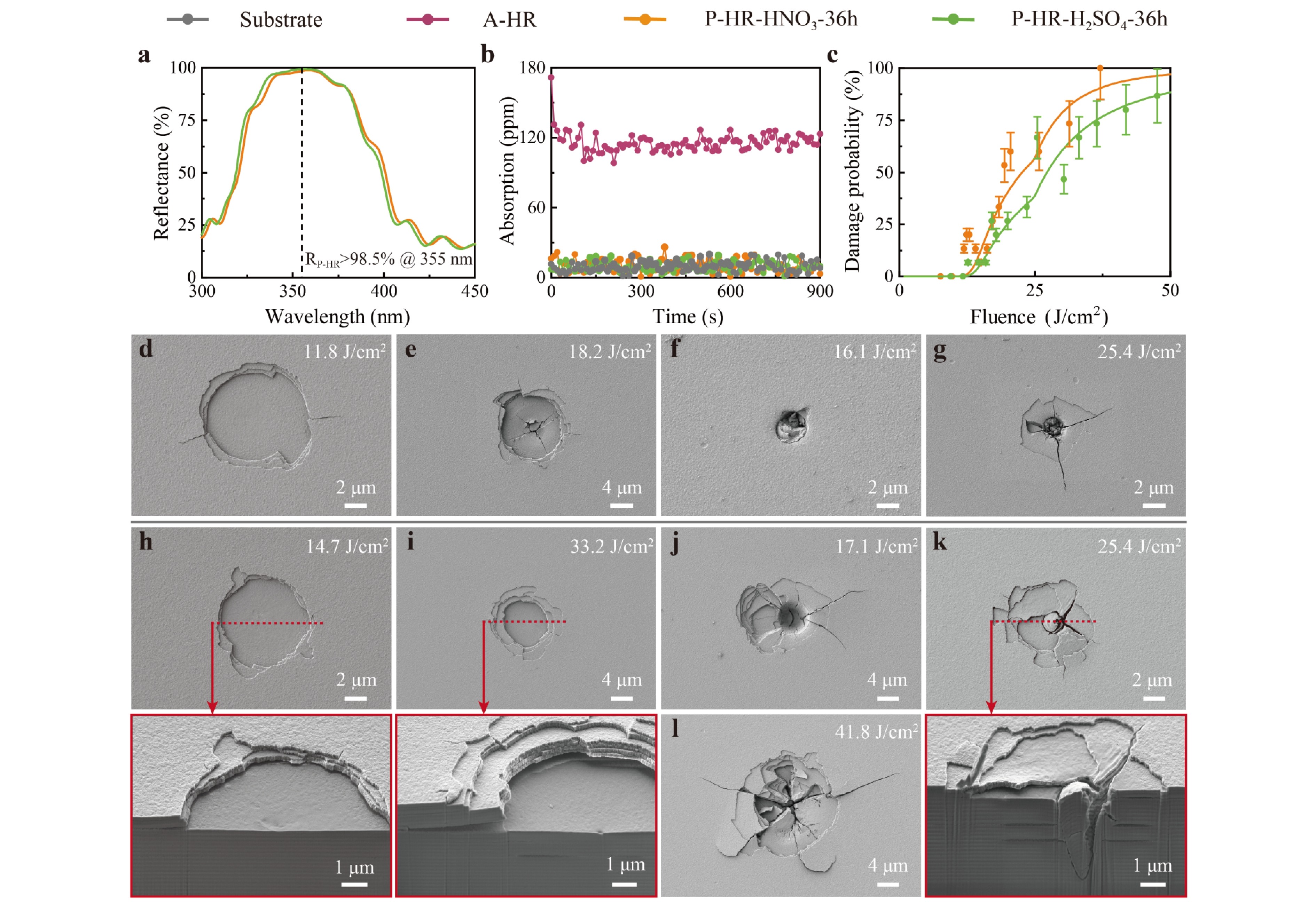
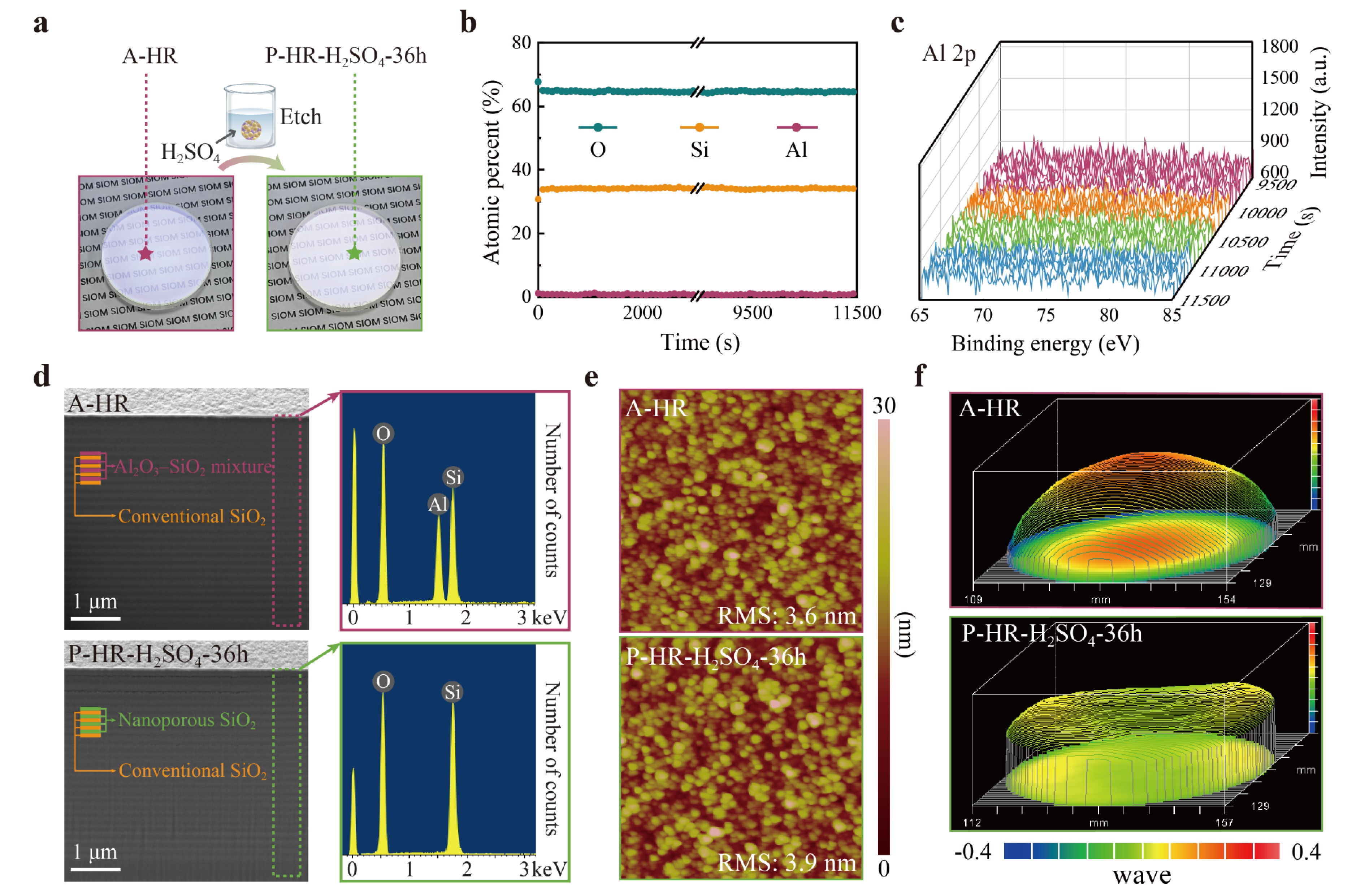
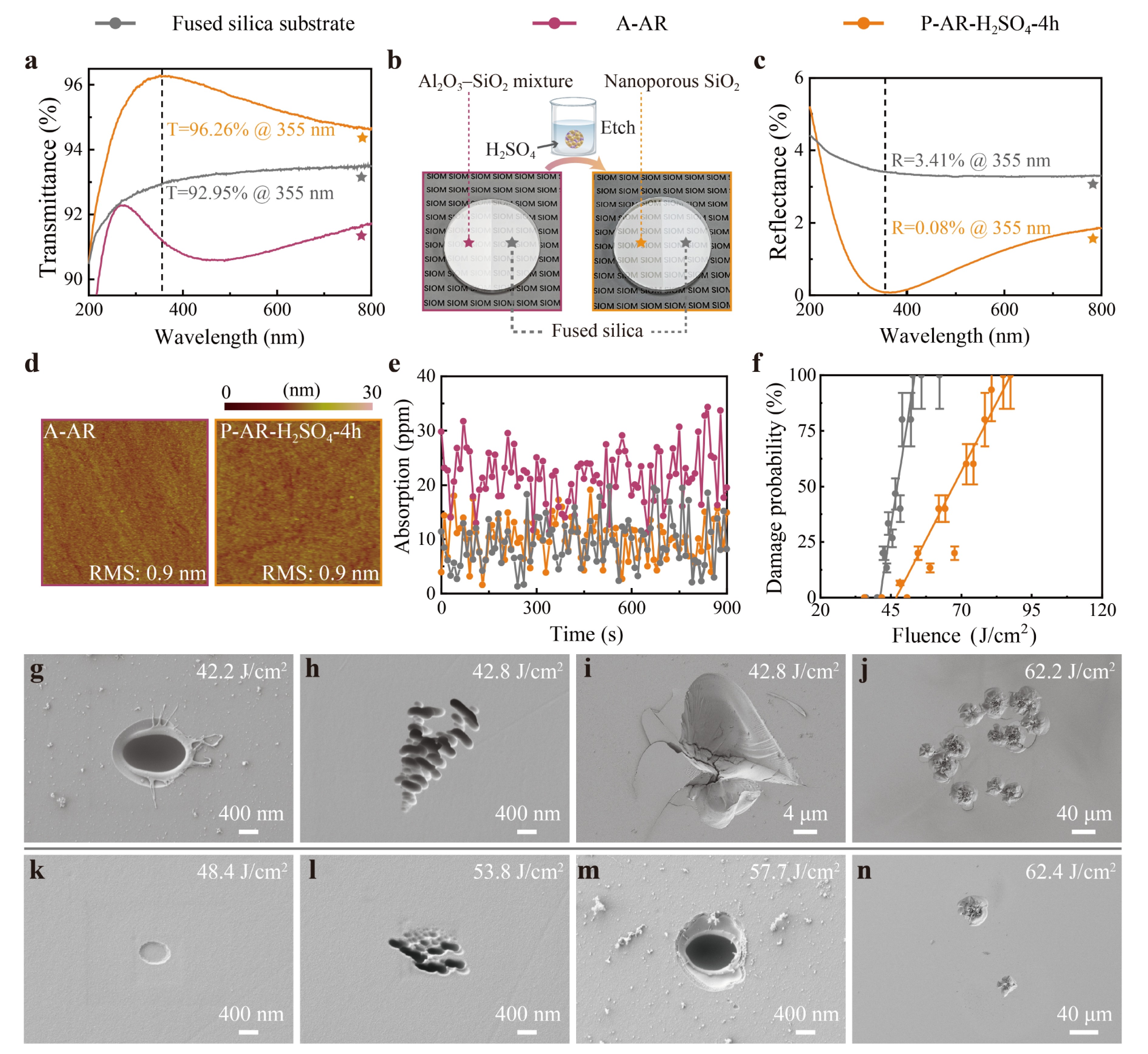
Laser-resistant coatings are becoming increasingly essential to meet the growing demand for high-power lasers. The laser-induced damage threshold (LIDT) of coatings can be significantly improved by constructing dielectric coatings that contain both high-refractive-index (high-n) and low-n layers made from SiO2-based materials with a wide bandgap and low absorption, specifically dense and porous SiO2. This study proposes and demonstrates the fabrication of all-silica laser-resistant anti-reflection (AR) and high-reflection (HR) coatings using a combination of plasma-ion-assisted electron-beam co-evaporation of Al2O3–SiO2 mixtures, followed by selective chemical etching. The suitability of this method for producing large-size single-layer and multilayer coatings was verified experimentally. The porous SiO2 layer exhibited absorption properties comparable to those of a fused silica substrate. Both AR and HR coatings exhibited good laser resistance at a wavelength of 355 nm. Notably, the LIDT of the AR coating (~46.9 J/cm2) exceeded that of the fused silica substrate (~41.1 J/cm2). The proposed fabrication method is simple, cost-effective, and holds great promise for advancing the development of high-performance laser coatings.
Published. 2026, 7(3)
: 712-721
doi: 10.37188/lam.2026.034
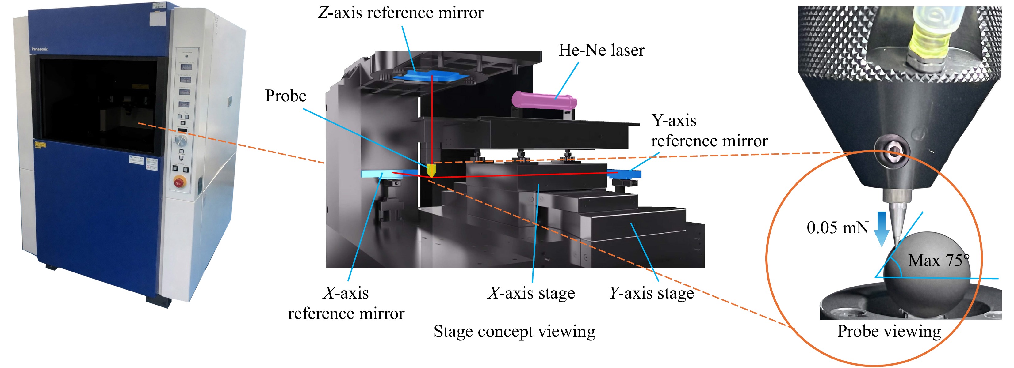
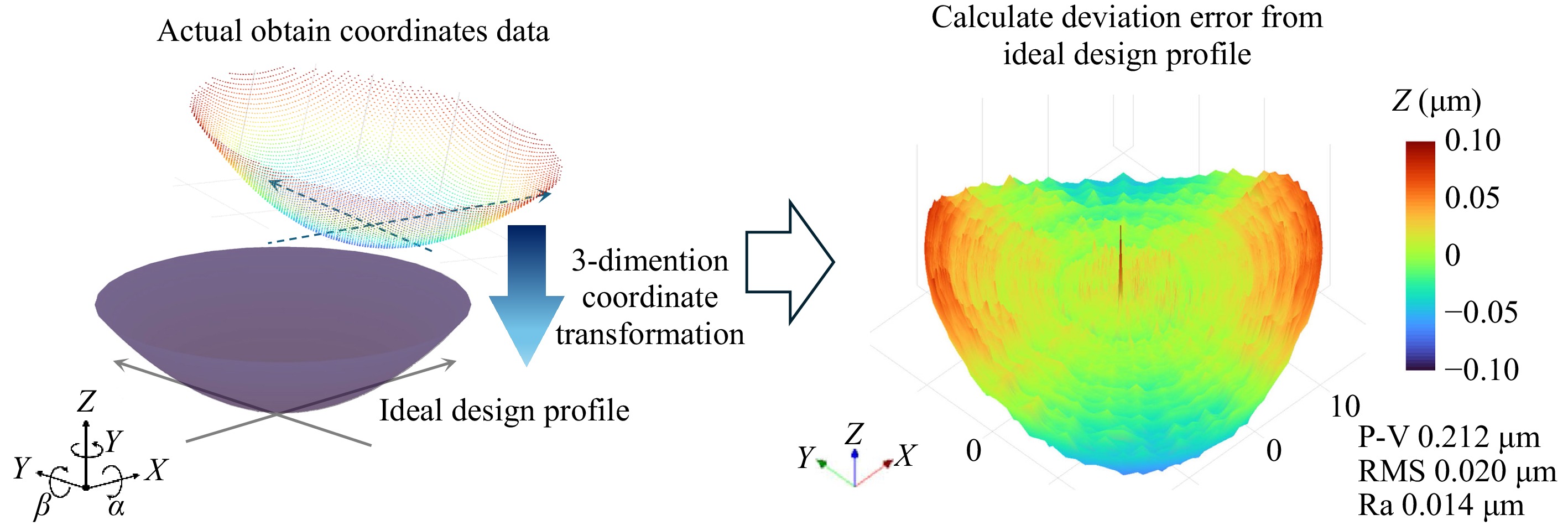
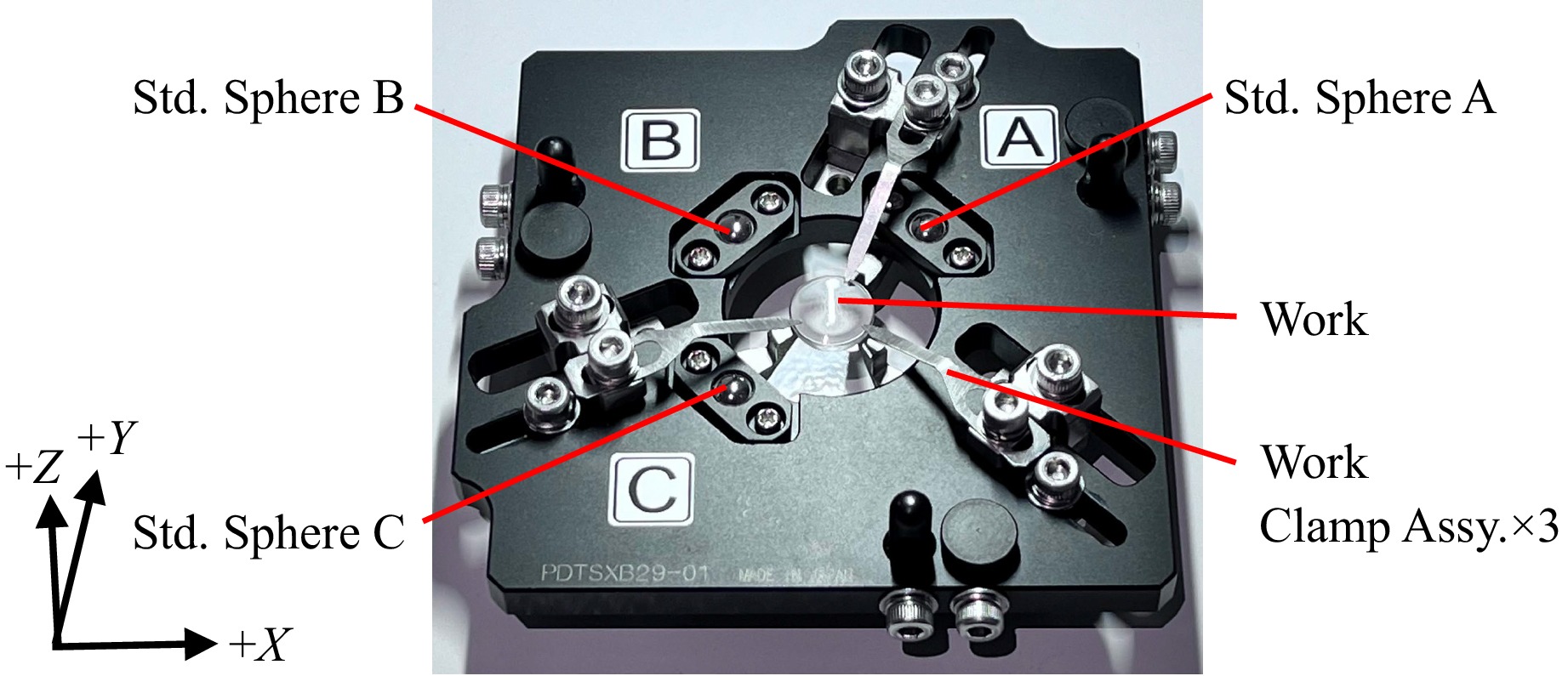
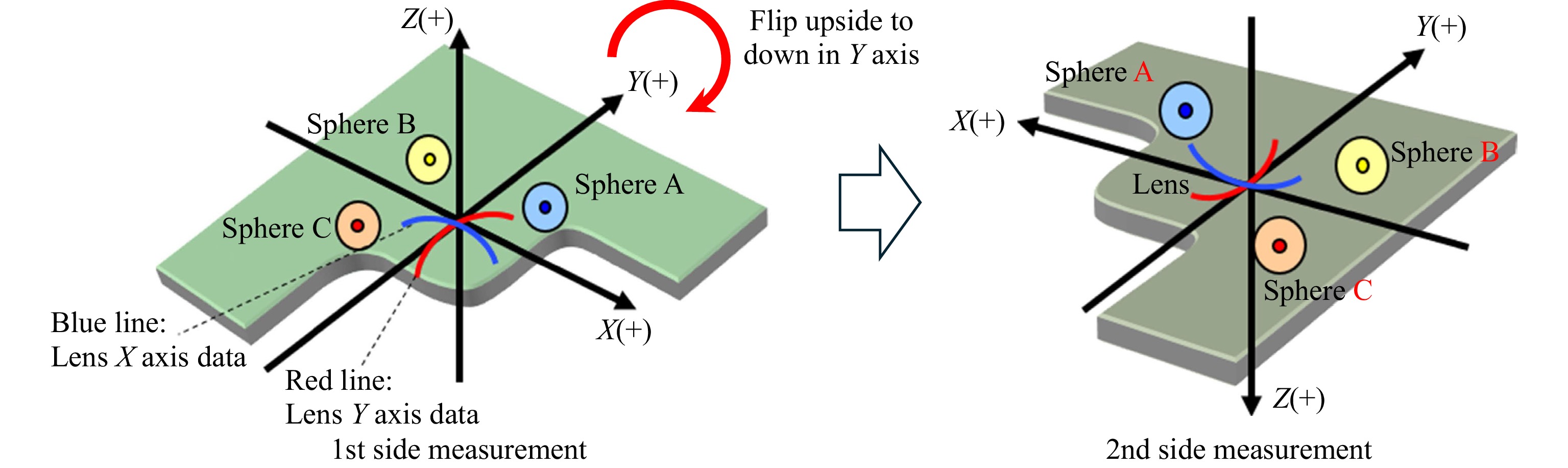
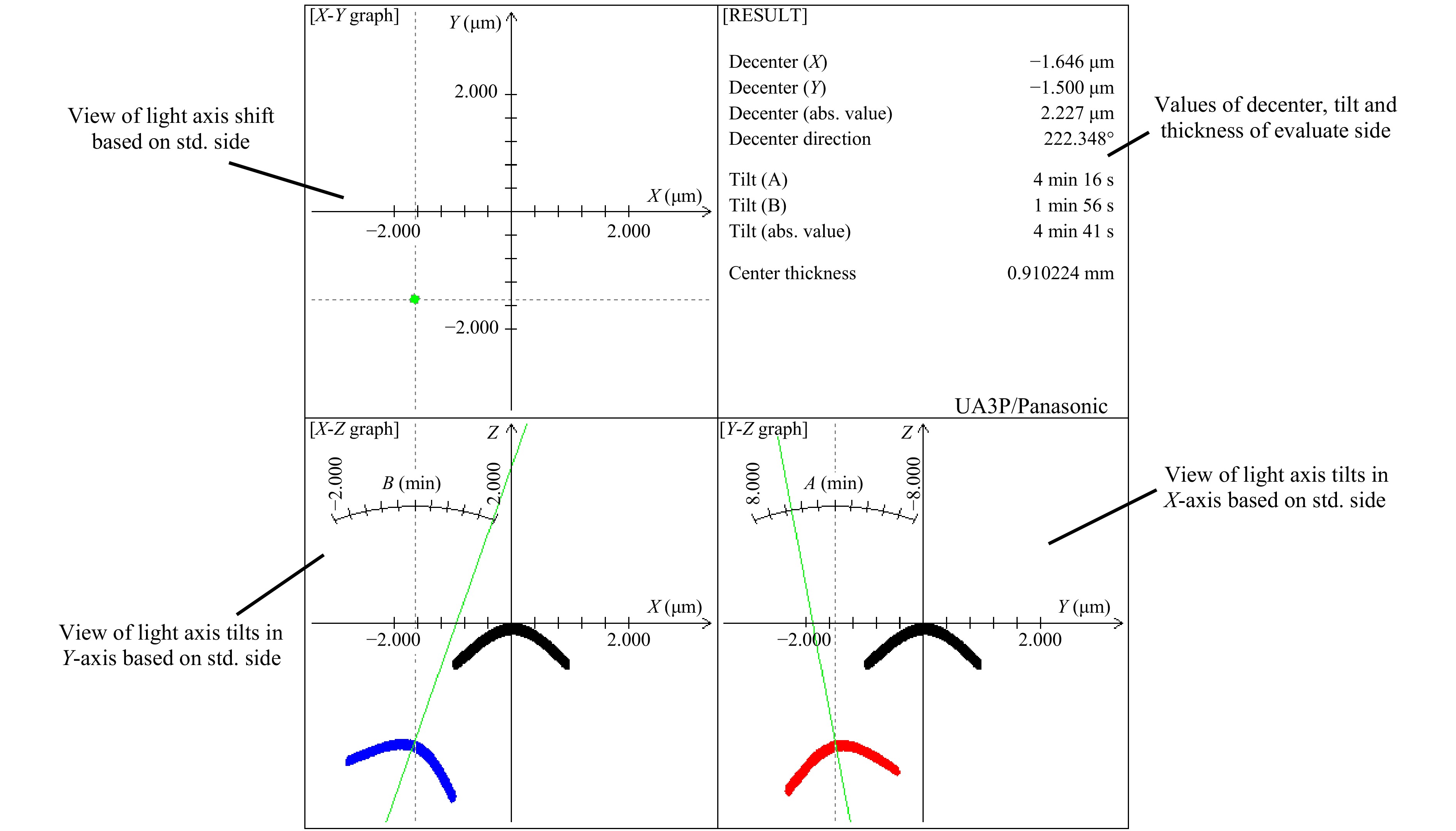
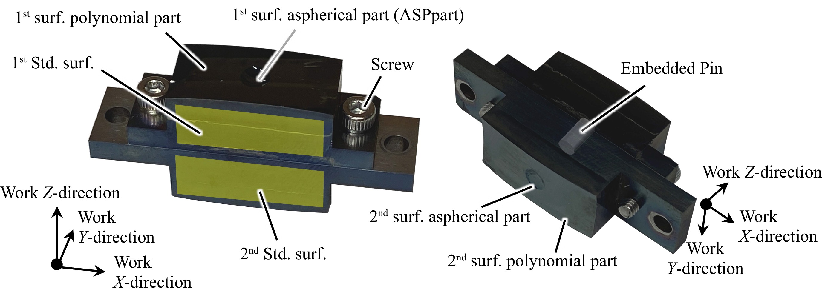
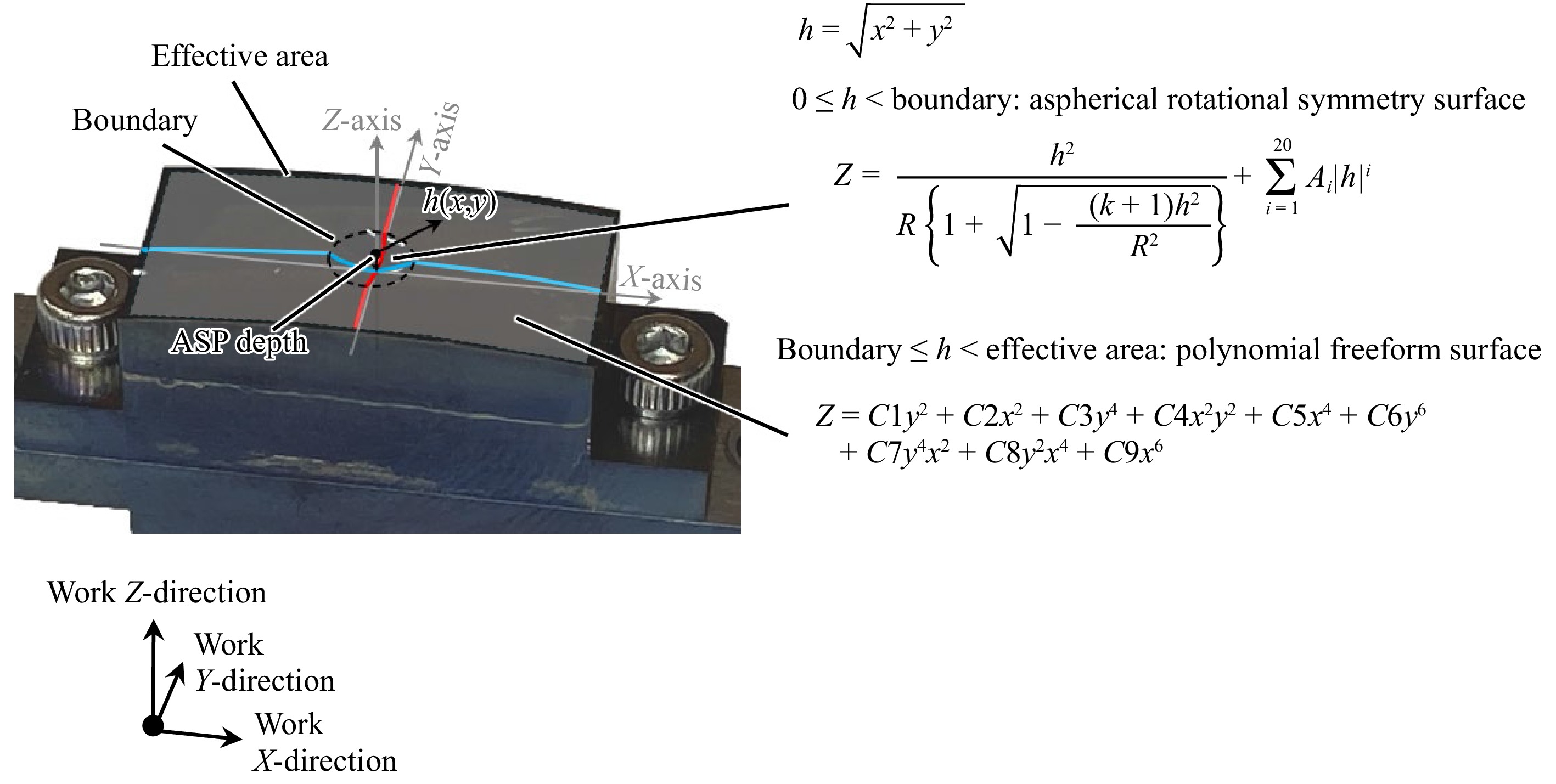
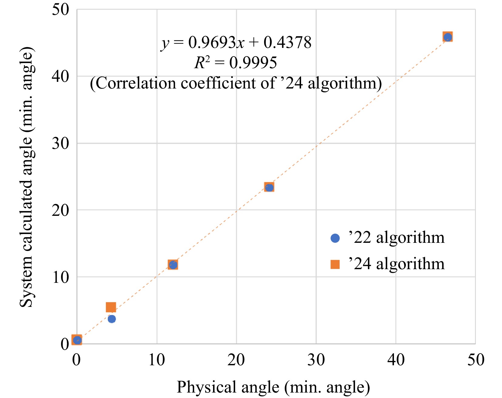
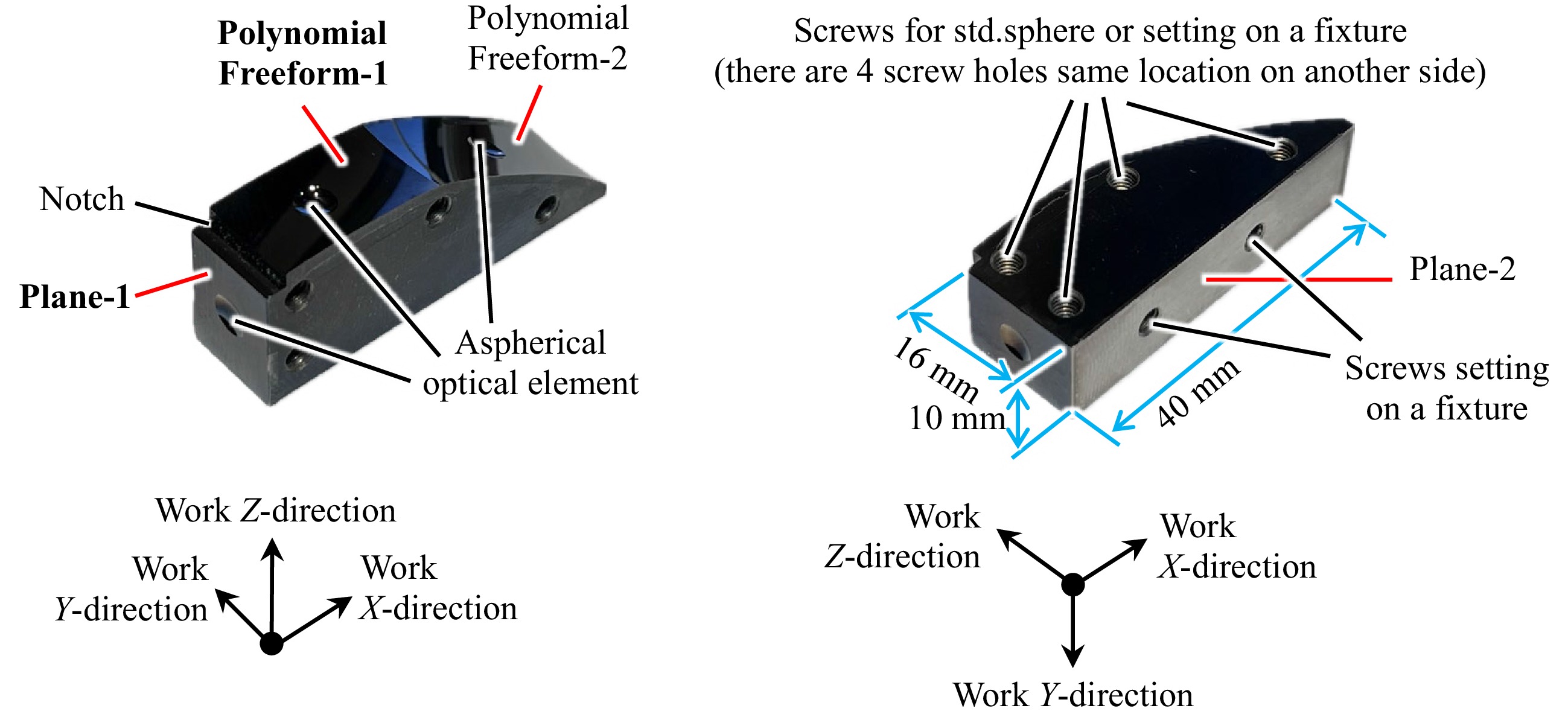
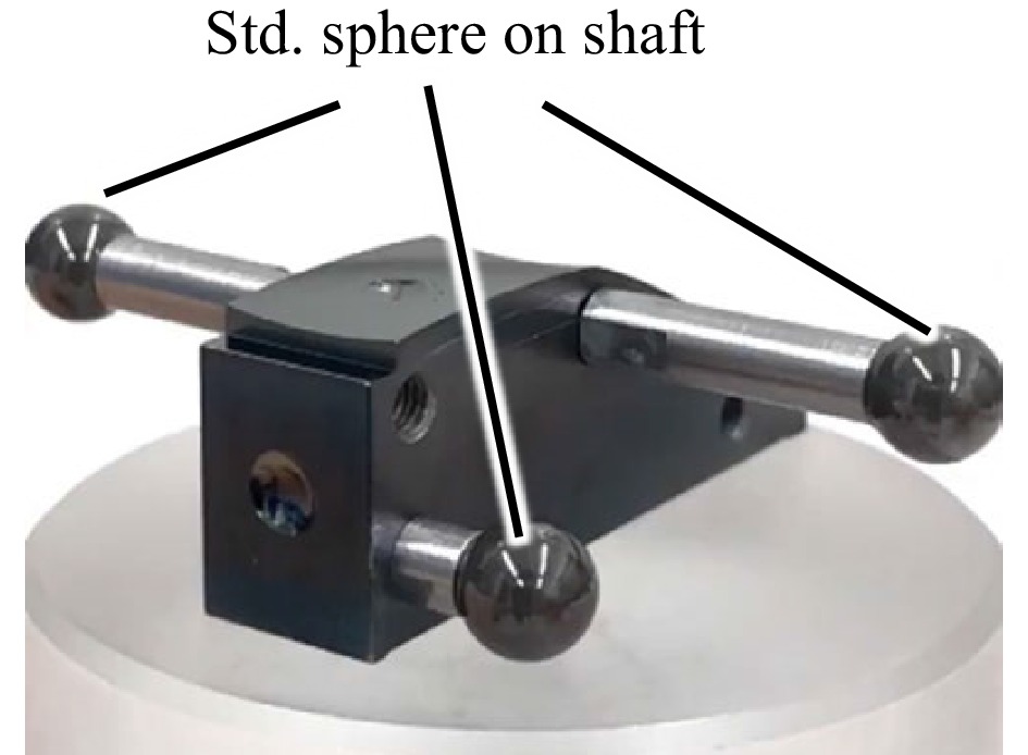
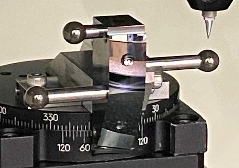
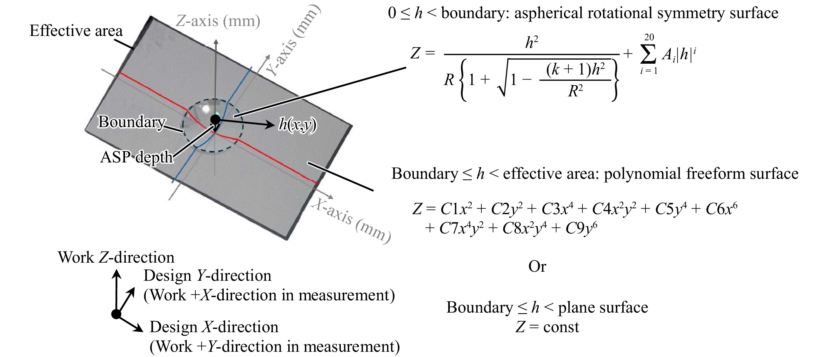
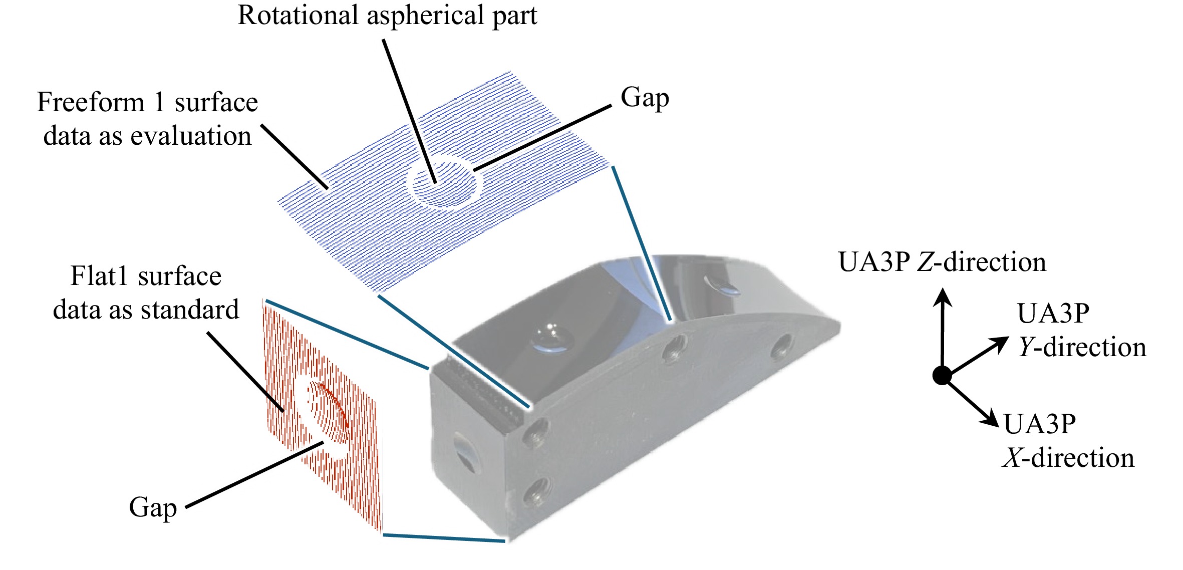
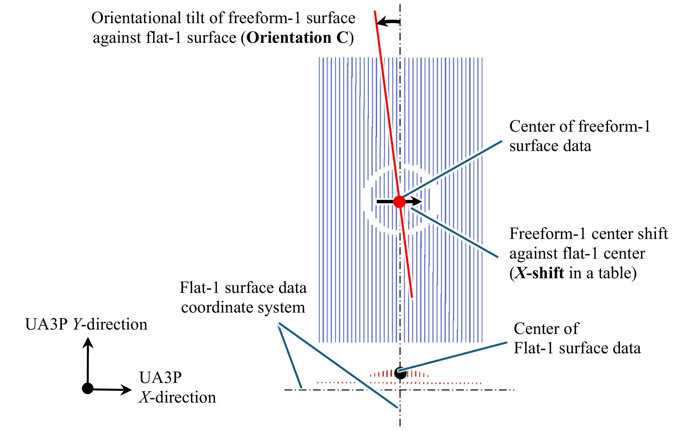
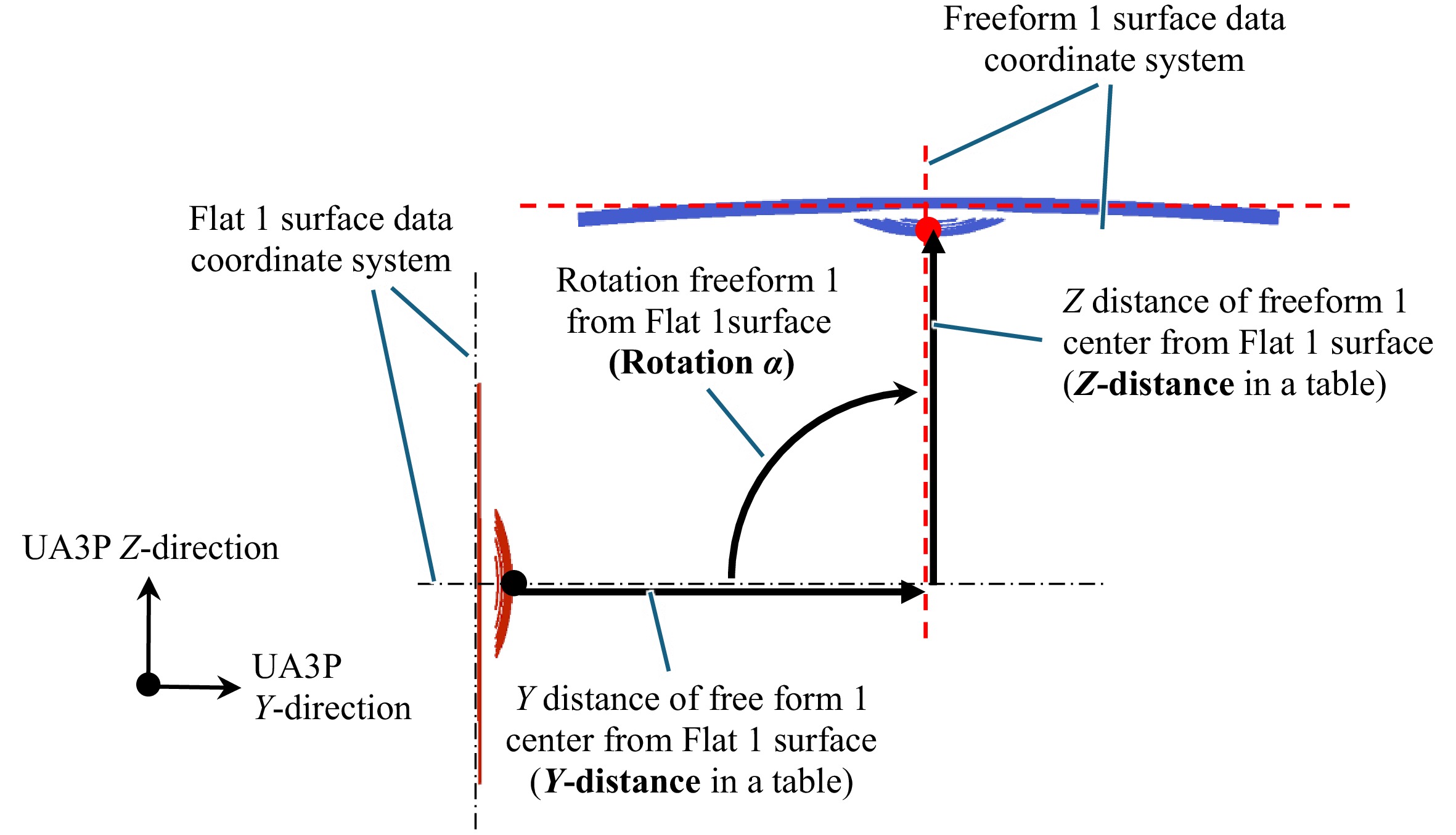
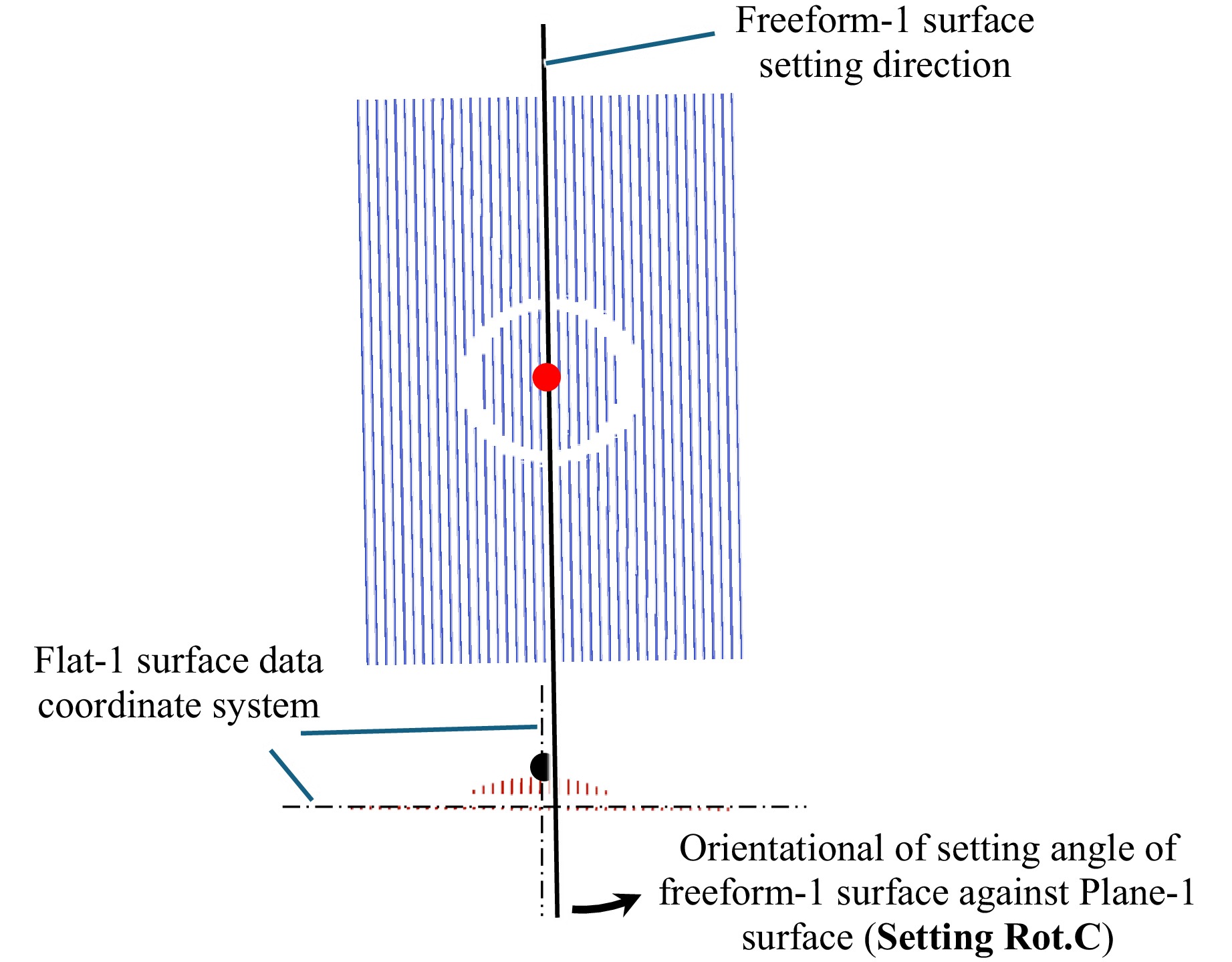
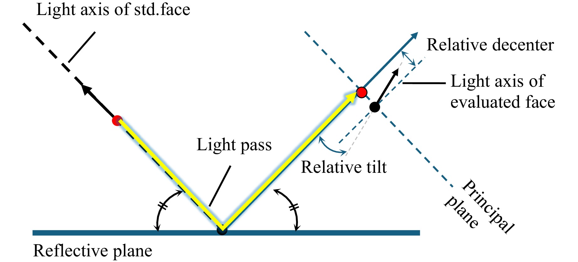
With the rapid growth of extended-reality (XR) devices, simultaneously achieving long optical path length and miniaturization has become a central challenge in optical system design. One promising approach is to employ optical designs that utilize multiple internal reflections in a prism to extend the path length within a compact volume. The prisms targeted in this study are polyhedral elements composed of three or more optical surfaces including freeform surfaces, in which two lateral faces are mutually parallel. A representative example is a triangular prism whose optical faces are replaced by freeform surfaces. Because such prisms contain multiple reflecting faces, their inter-surface positional relationships must be formed and maintained with high accuracy; consequently, metrology capable of precise evaluation of face-to-face position is indispensable for production. Since 2002, Panasonic has introduced to the market inter-surface misalignment evaluation of lens surfaces using the ultra-high-accuracy three-dimensional profilometer UA3P, contributing to higher-precision camera modules. Building on that platform, the present work develops a new measurement method that extends the UA3P system to prisms with multiple reflecting faces, enabling spatial registration to be evaluated with an accuracy of 0.2–0.3 µm. The developed system shows strong correlation with existing methods and validated repeatability, demonstrating its suitability for high-precision manufacturing and quality assurance of optical elements, including prisms for XR devices.
Published. 2026, 7(3)
: 722-735
doi: 10.37188/lam.2026.064
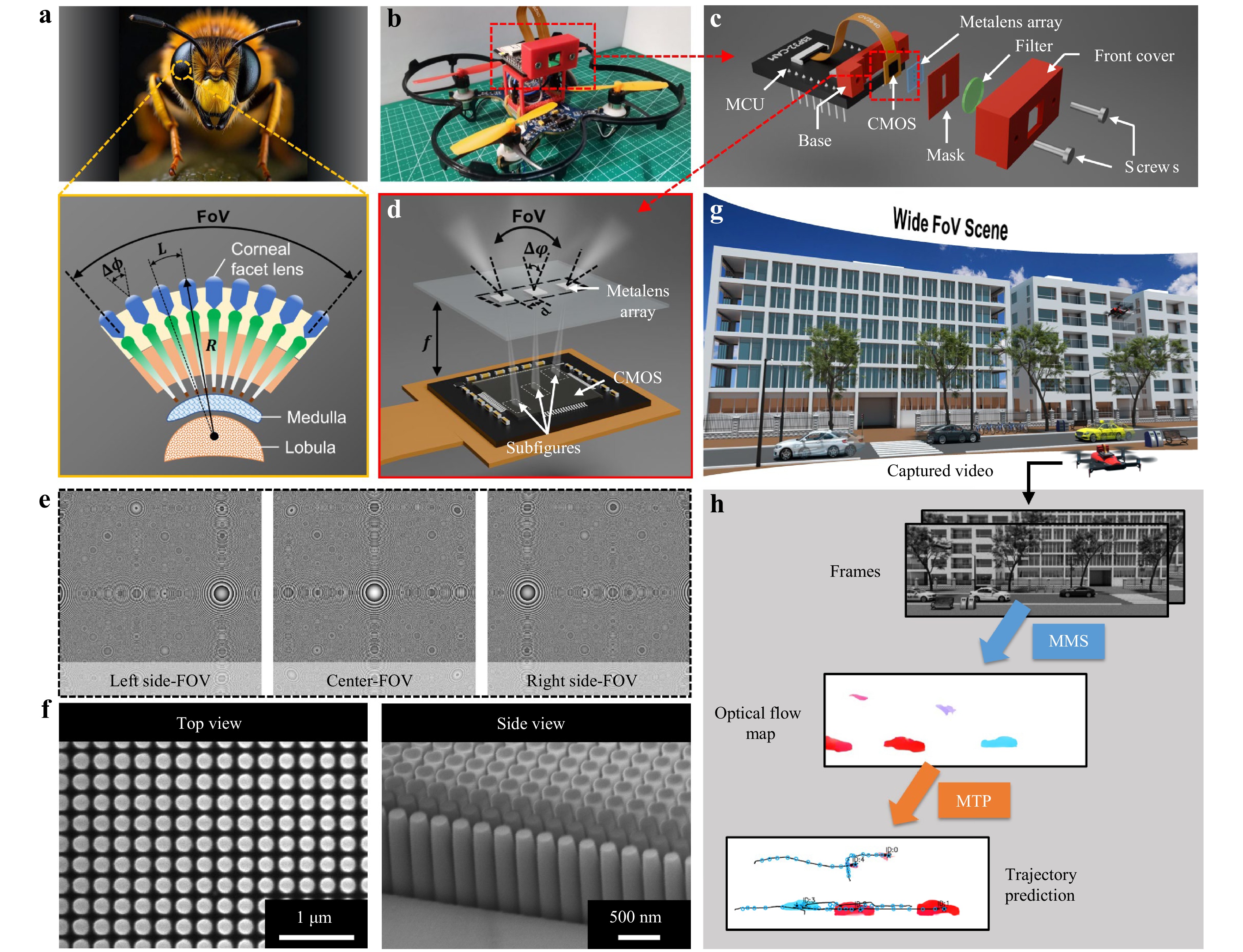
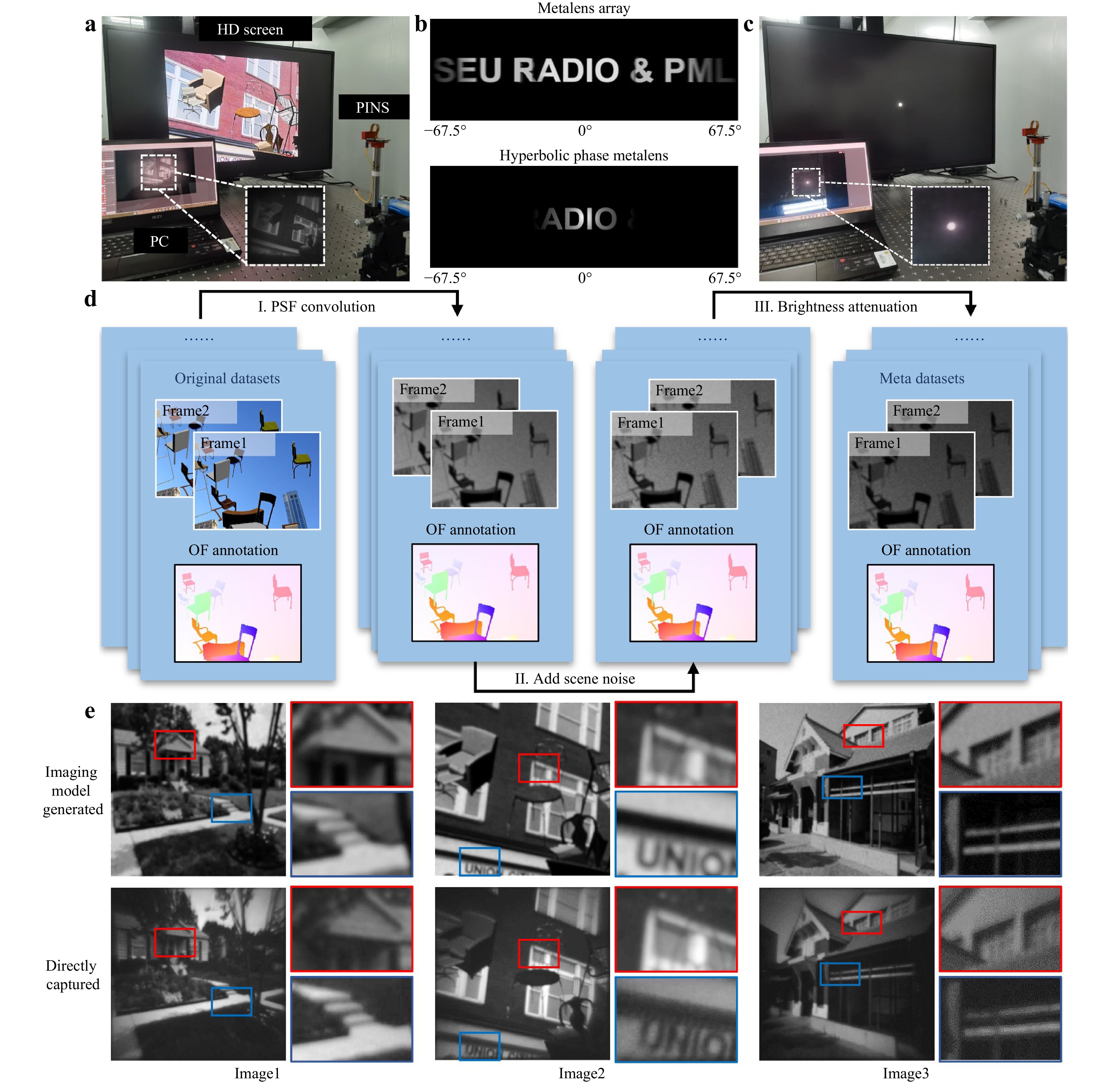
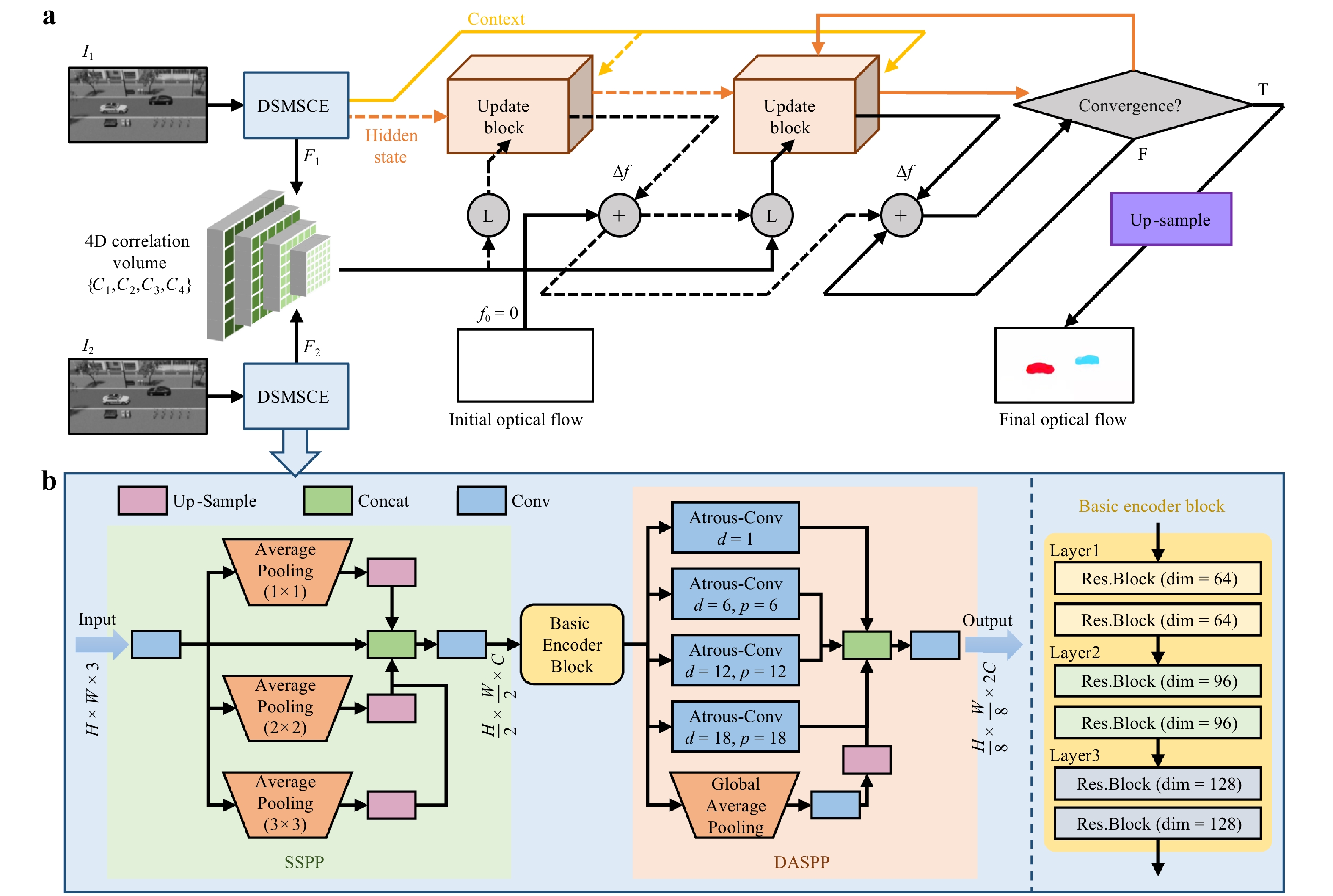
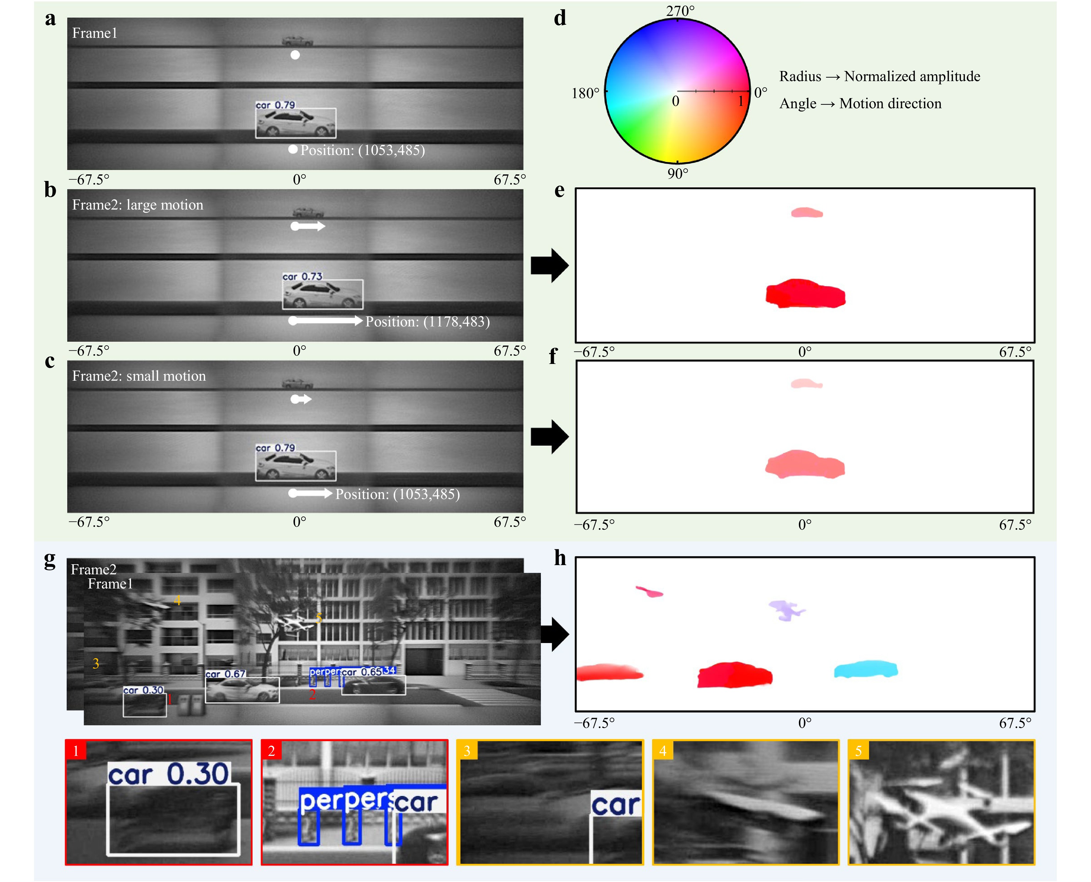
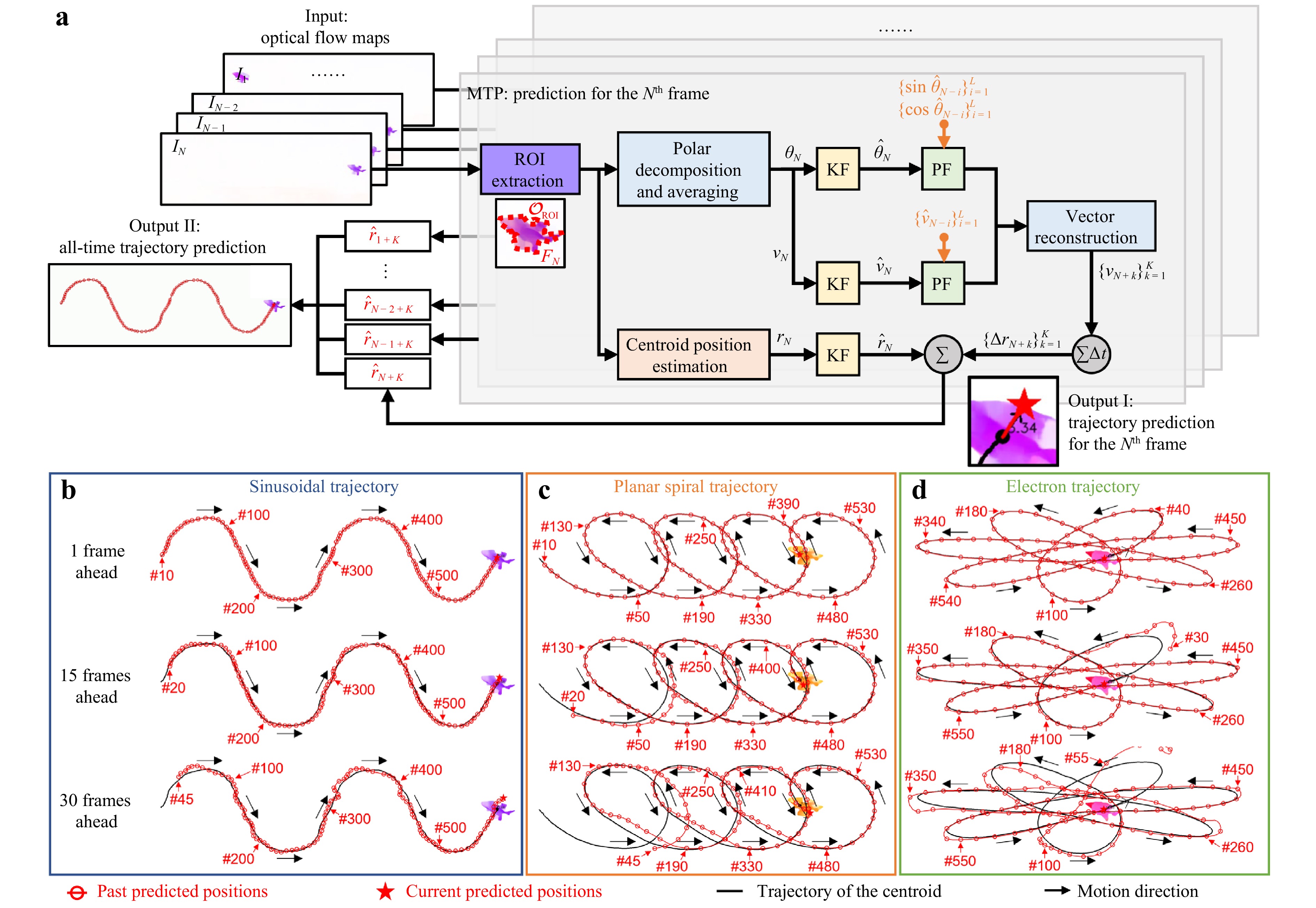
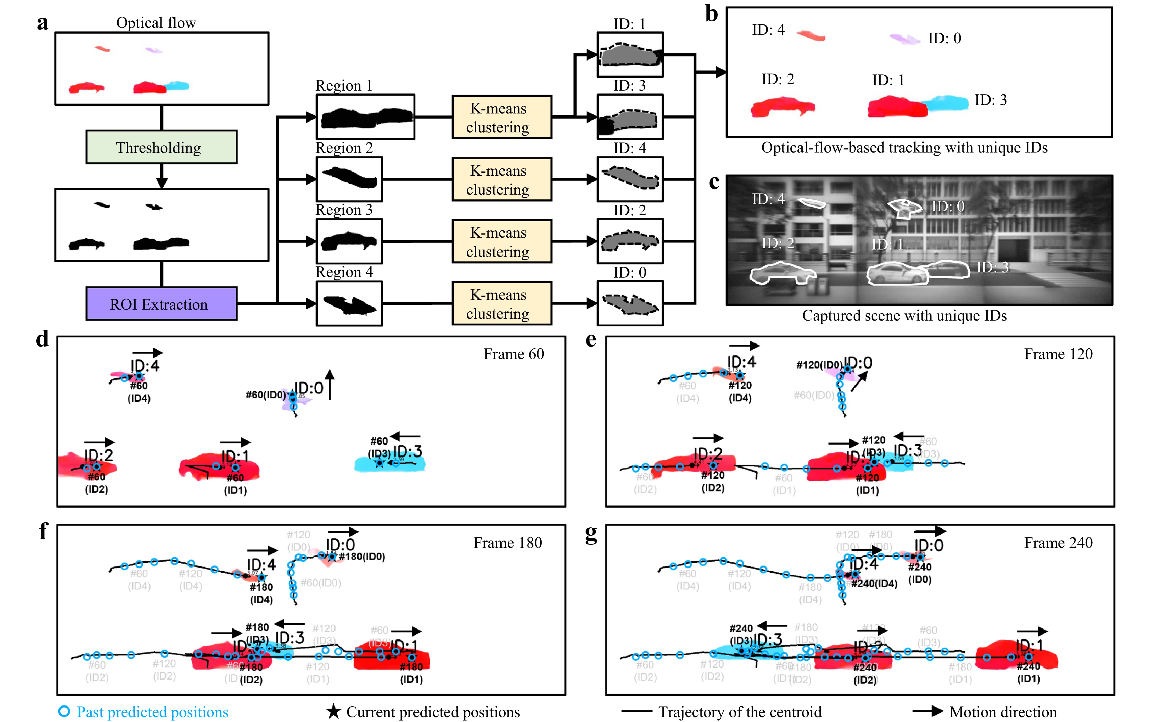
In nature, certain insects possess specialised compound eye structures that provide an ultra-wide field-of-view (FoV) and rapid response capabilities, enabling them to capture prey and avoid obstacles. Herein, inspired by compound eyes, a planar intelligent nanophotonic sensor (PINS) based on a metalens array, which possesses an ultrawide horizontal FoV exceeding 135°, is demonstrated. By leveraging a deep neural network, meta-motion sense (MMS), accurate optical flow can be extracted from PINS-captured wide-FoV scenes, enabling a comprehensive characterisation of the motion velocities and directions of all dynamic objects. Compared to traditional machine-vision-based object recognition algorithms, the proposed approach exhibits significantly higher accuracy and robustness, particularly in detecting small, slow, or background-blended moving targets, and offers an intelligent predictive capability for forecasting the motion trajectories of objects. The proposed device combines the advantages of high compactness, superior motion-detection performance, and intelligent functionality, offering a promising foundation for next-generation applications in autonomous navigation, situational awareness, and military surveillance.
Published. 2026, 7(3)
: 736-746
doi: 10.37188/lam.2026.056
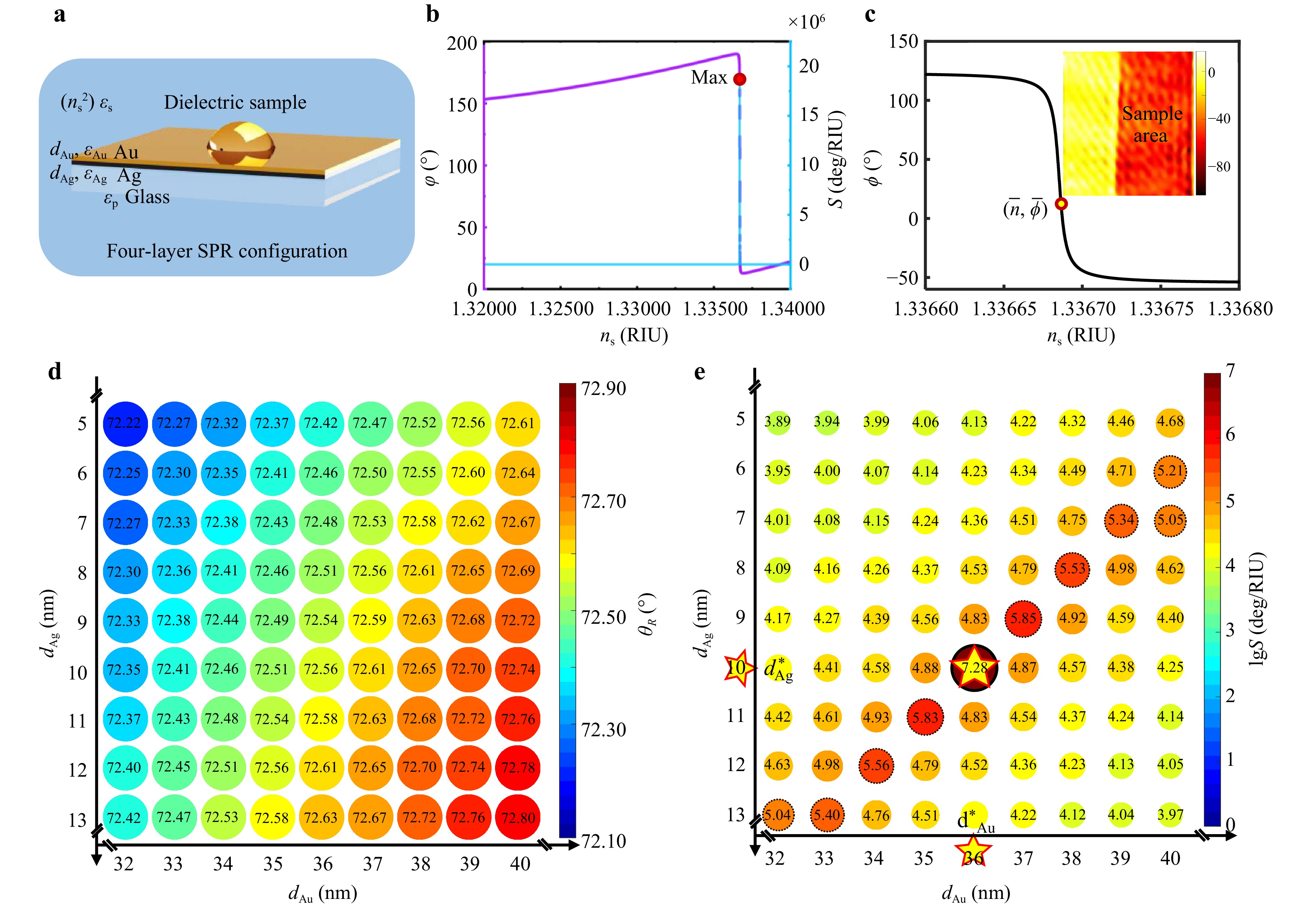
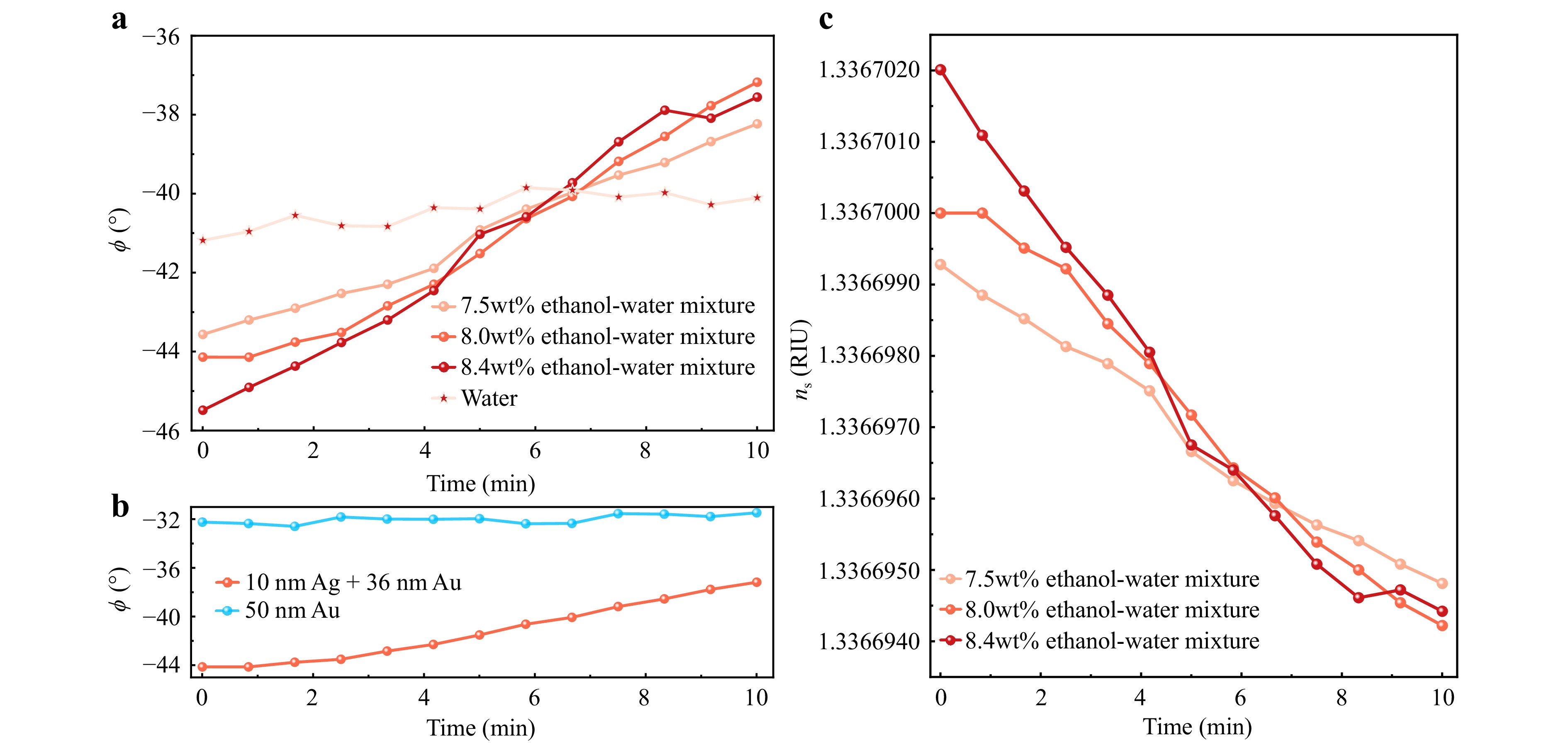
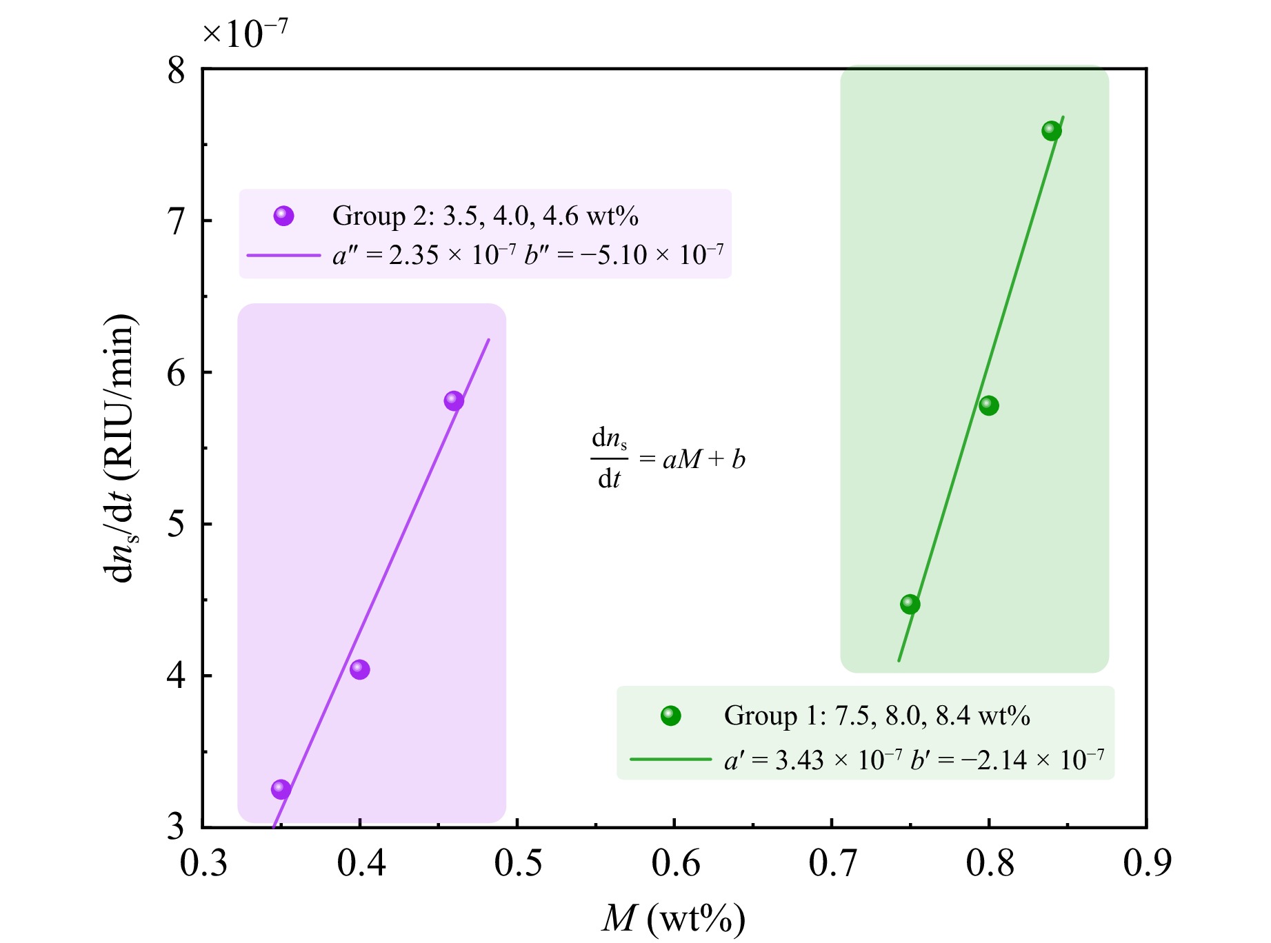
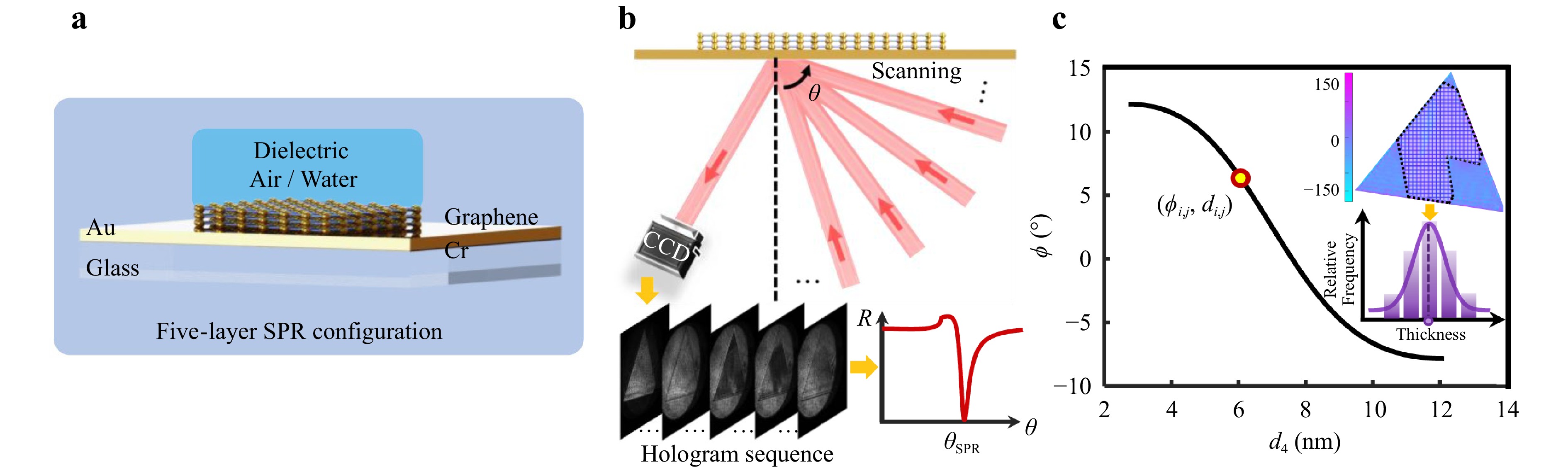
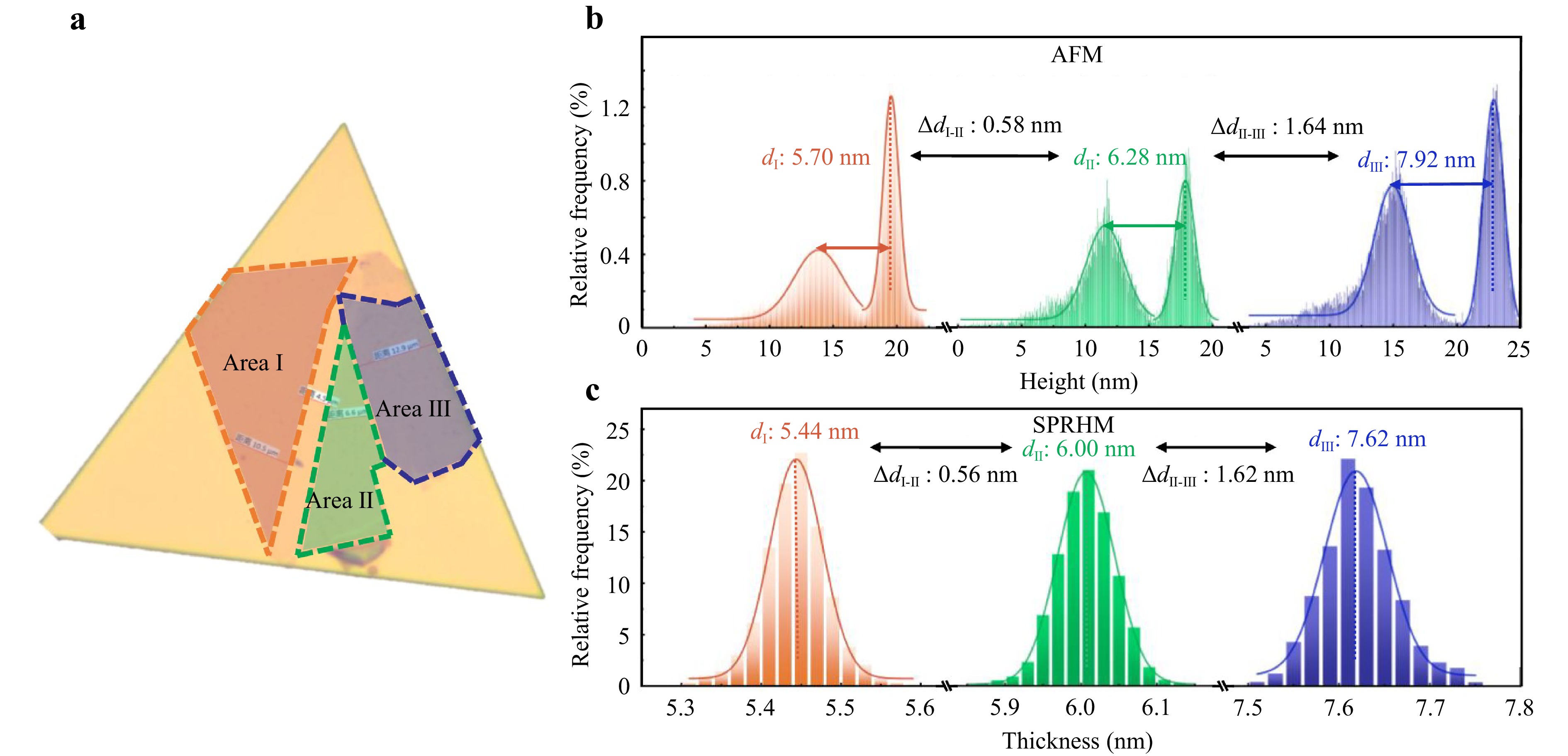
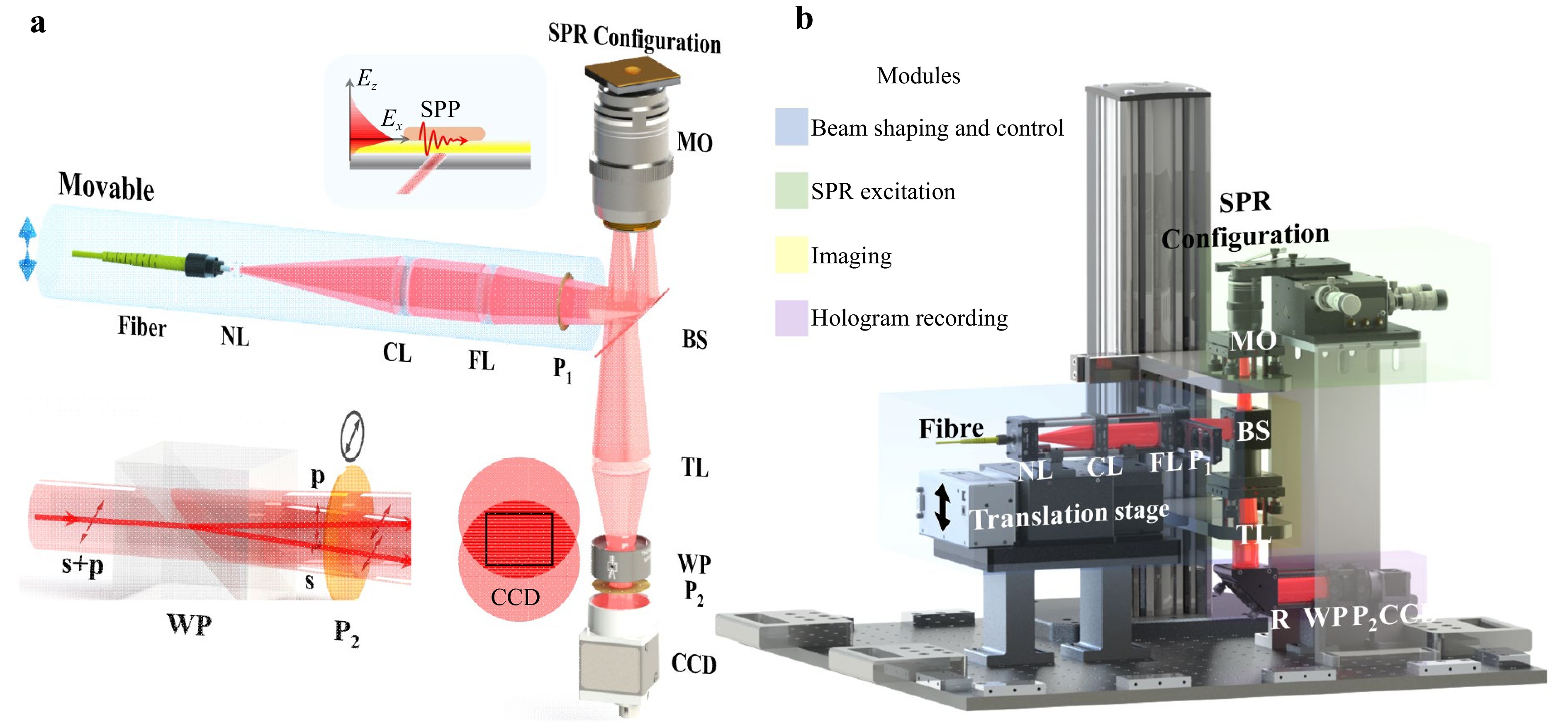
Employing optical microscopy for visualisation and quantification of dielectric analytes in the near-field area has been a persistent objective, connecting nanoscale dynamics with macroscopic phenomena. Surface plasmon resonance holographic microscopy (SPRHM) leverages evanescent-field interactions and digital holography to enable label-free wide-field quantitative intensity and phase imaging of the near-field area, emerging as a flexible optical tool for high-throughput visualisation and characterization of chemical reactions. However, current SPRHM demodulation methods remain insufficient to meet the growing demand for a higher measurement sensitivity. Here, we introduce an optimised Ag–Au bilayer SPR excitation configuration and angle-scanning thickness demodulation workflow, designed to achieve ultrahigh-sensitivity Refractive index (RI) and thickness measurements, respectively. Experiment results demonstrate the superior performance of the proposed methods: monitoring of RI variations of ethanol-water evaporation dynamics with a resolution of 2.58 × 10⁻⁷ RIU and thickness profiling of a graphene terrace specimen with a step-height accuracy of 0.56 nm. Integrated with these advanced methods, we present a versatile SPR holographic microscope prototype that features minimal opto-mechanical complexity, and exceptional stability, enabling unprecedented observations of biomolecular interactions, nanomaterial optics, electrochemical dynamic processes, etc.
Published. 2026, 7(3)
: 747-760
doi: 10.37188/lam.2026.068
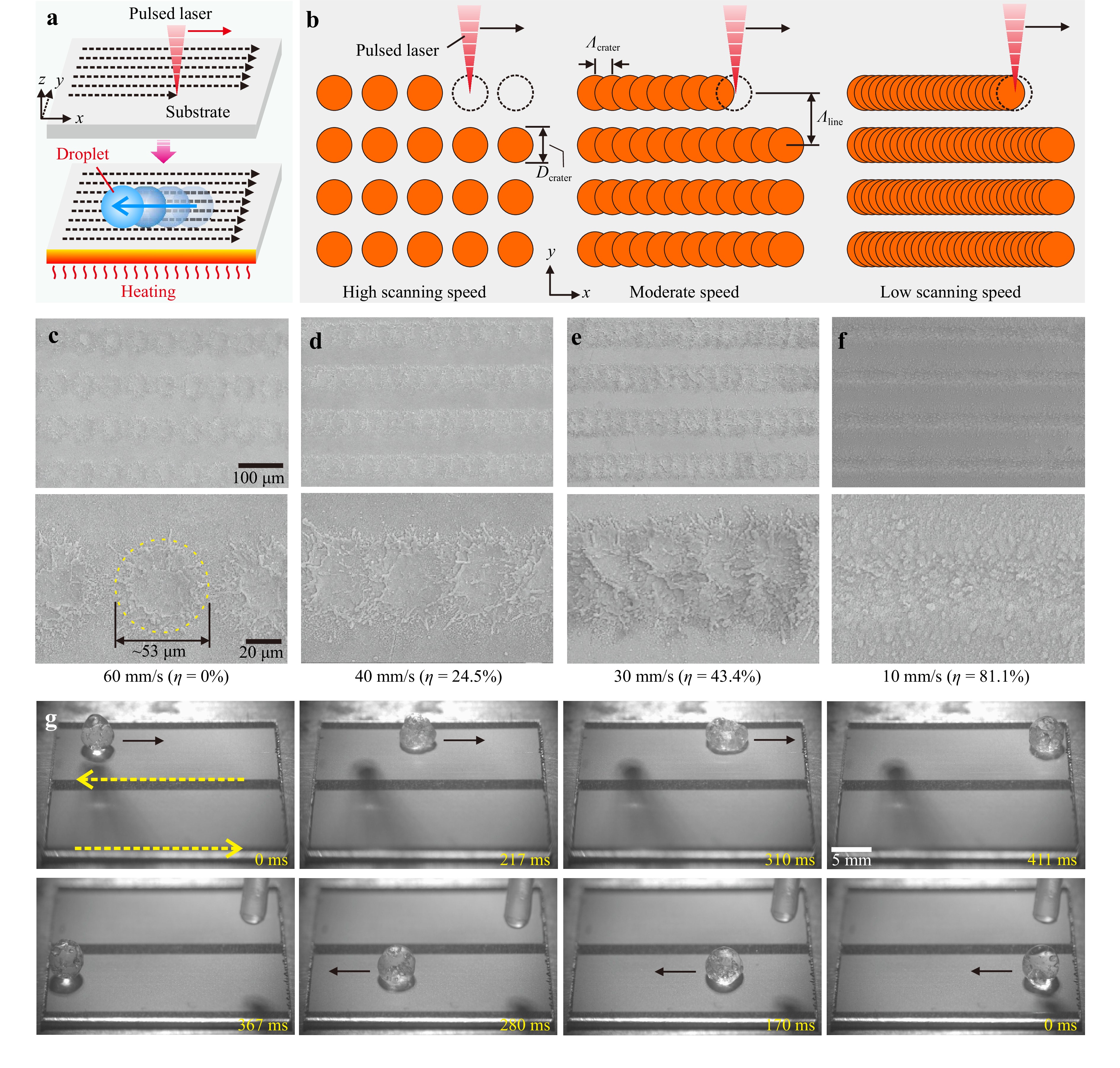
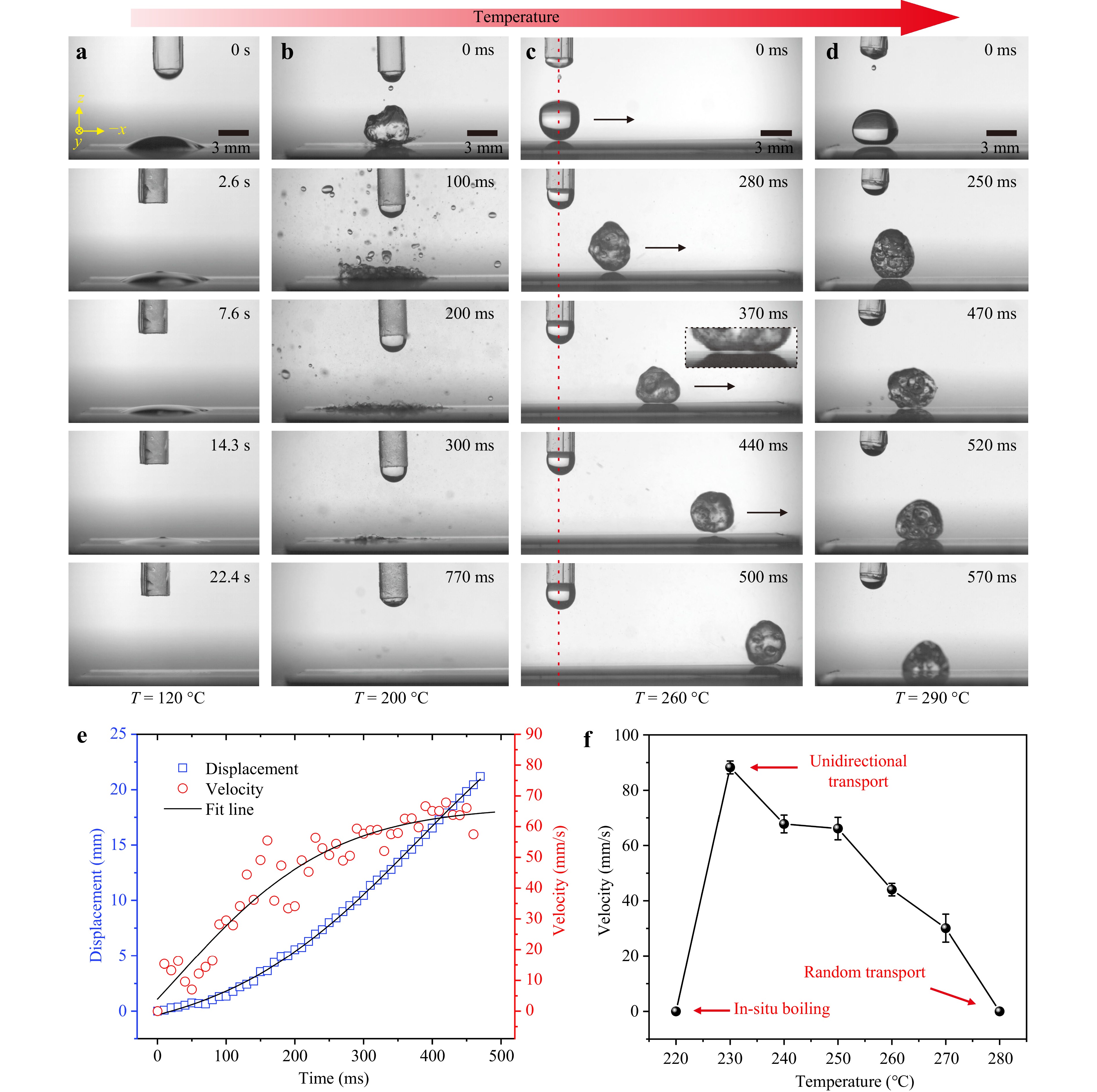
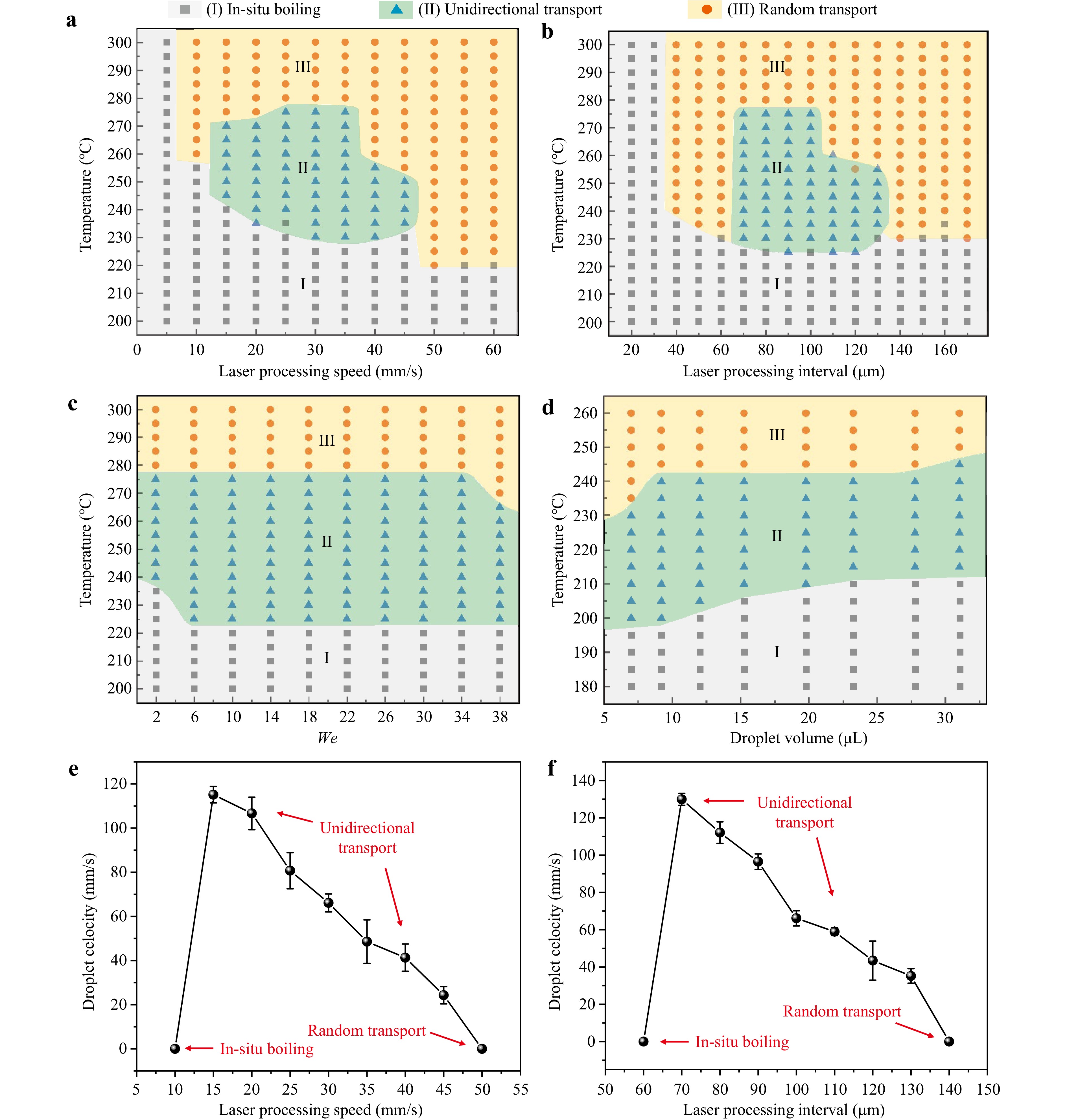
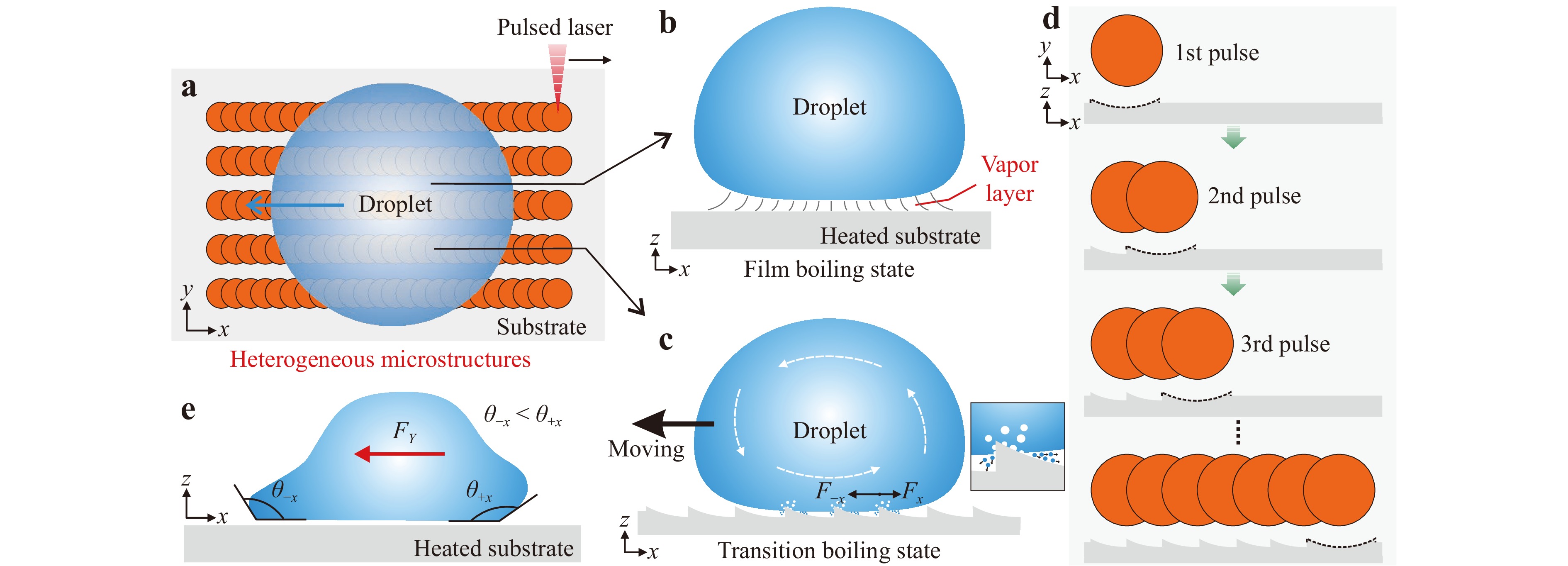
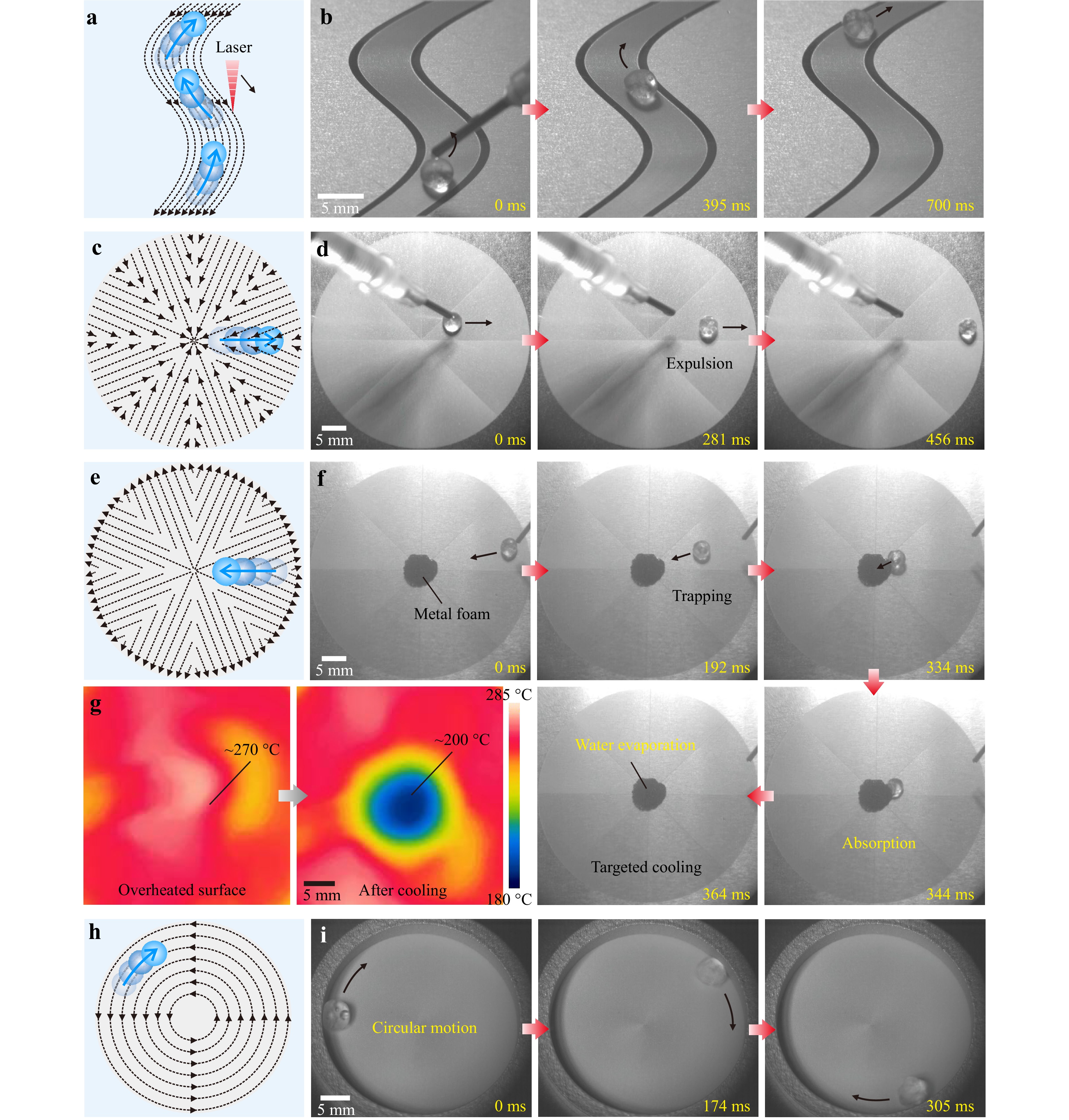
Liquid propulsion on overheated surfaces plays an important role in numerous engineering applications. However, most reported methods are limited to homogeneous asymmetric structures such as ratchet-shaped substrates. In this study, a dual heterogeneous structure is designed on an aluminium surface via femtosecond laser direct writing. The substrate surface is alternately covered with non-ablated smooth strips and laser-structured regions composed of periodic ripple microstructures. The droplets on the heated sheet exhibit a hybrid boiling state: film boiling in the smooth regions and intermittent transition boiling in the ripple microstructures. This hybrid state enables the droplets to remain in the Leidenfrost regime and combines the advantages of both the film- and transition-boiling states. The film-boiling regions facilitate the formation of a stable vapour cushion beneath the droplet, whereas the intermittent asymmetric contact boiling on the ripple microstructures produces a directional driving force and unidirectionally propels the Leidenfrost droplets. In particular, the droplets consistently move along the laser-scanning lines and opposite the laser processing direction. By ingeniously designing laser processing paths, diverse functions and applications of Leidenfrost droplet propulsion, including curved-path droplet transport, droplet expulsion, droplet trapping, targeted cooling, and droplet rotors, can be realised.

Published. 2026, 7(3)
: 761-778
doi: 10.37188/lam.2026.073
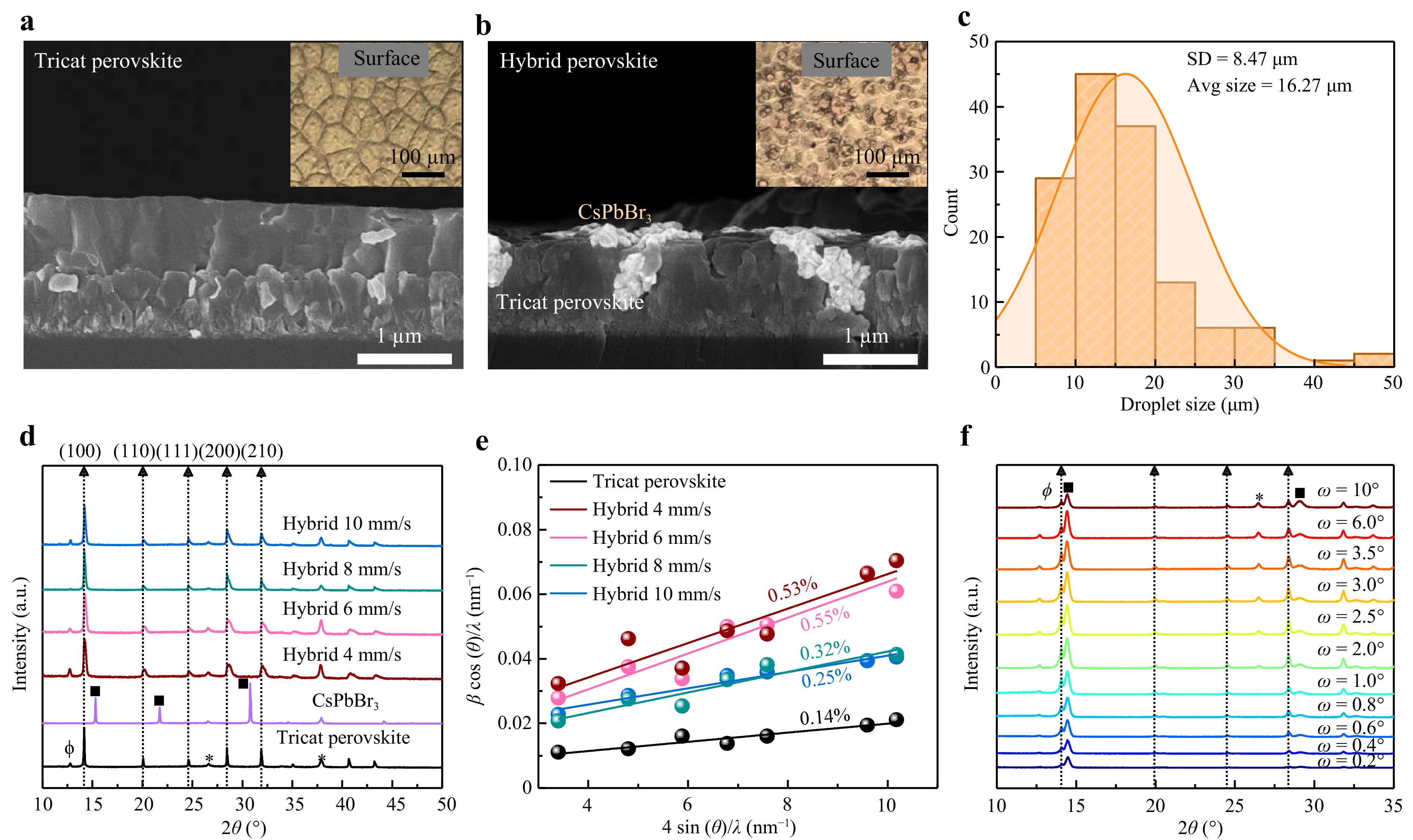
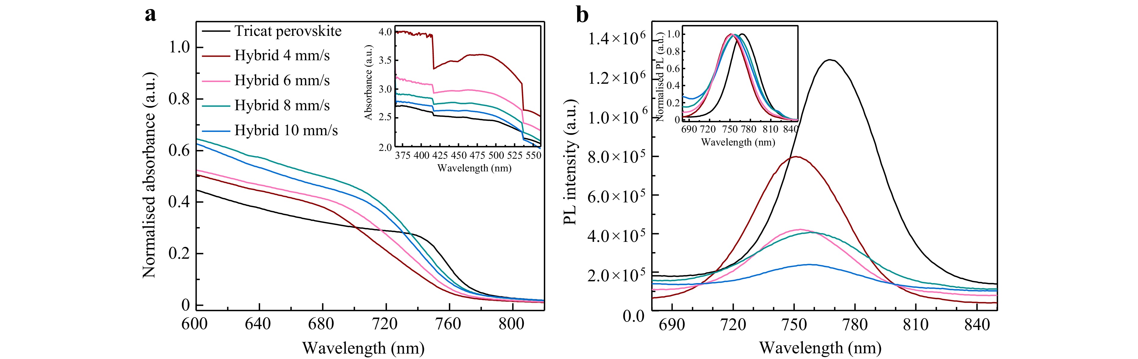
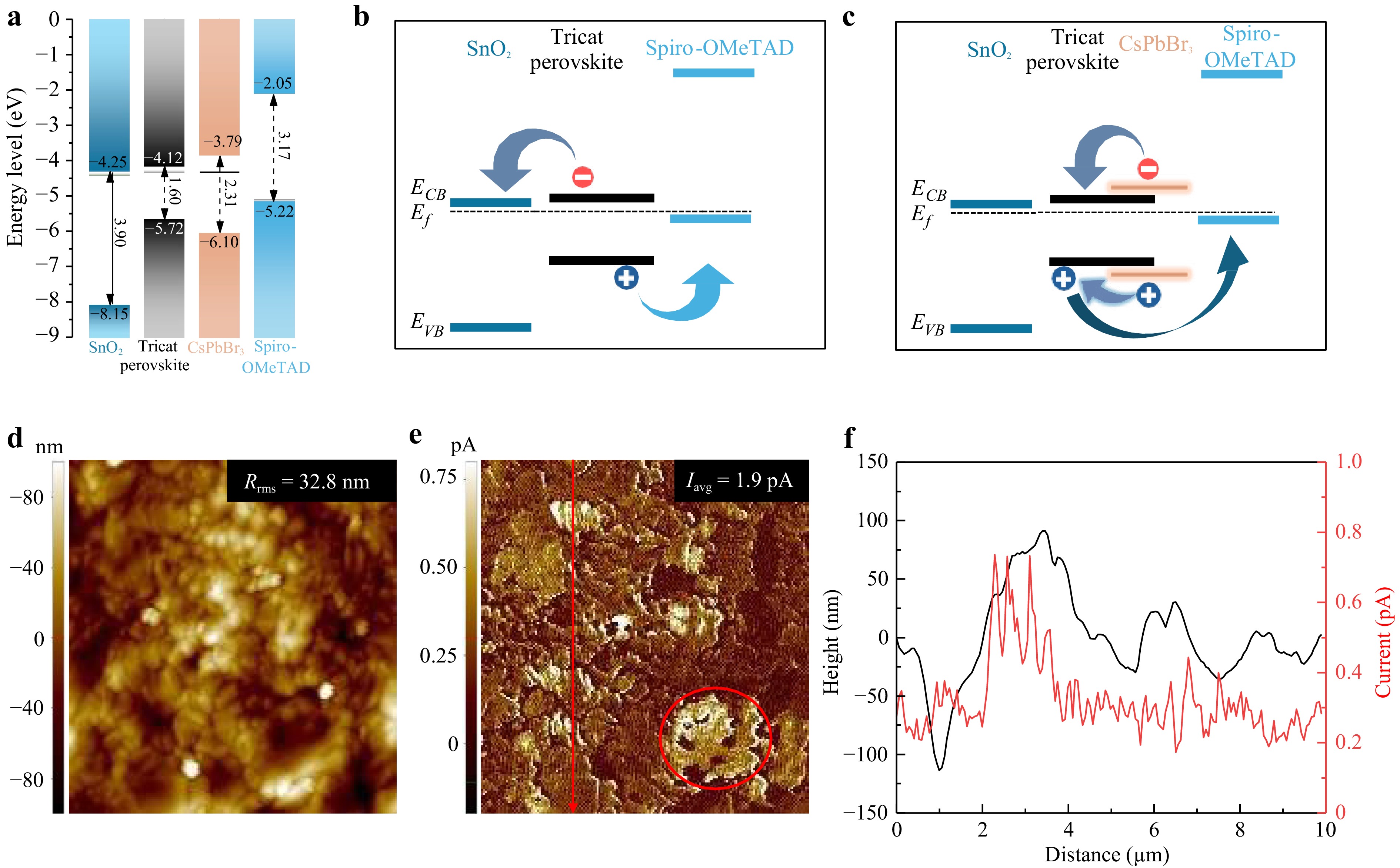
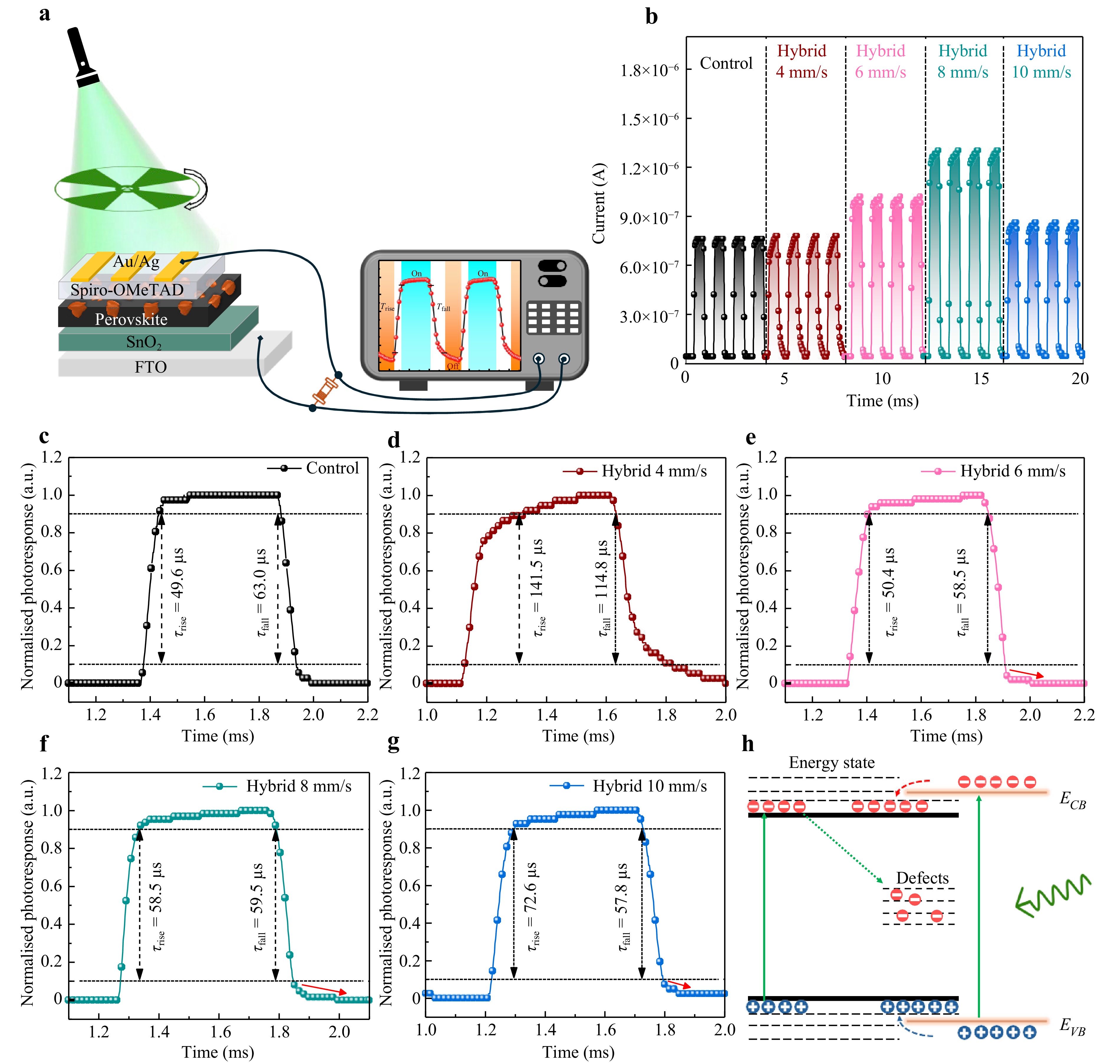
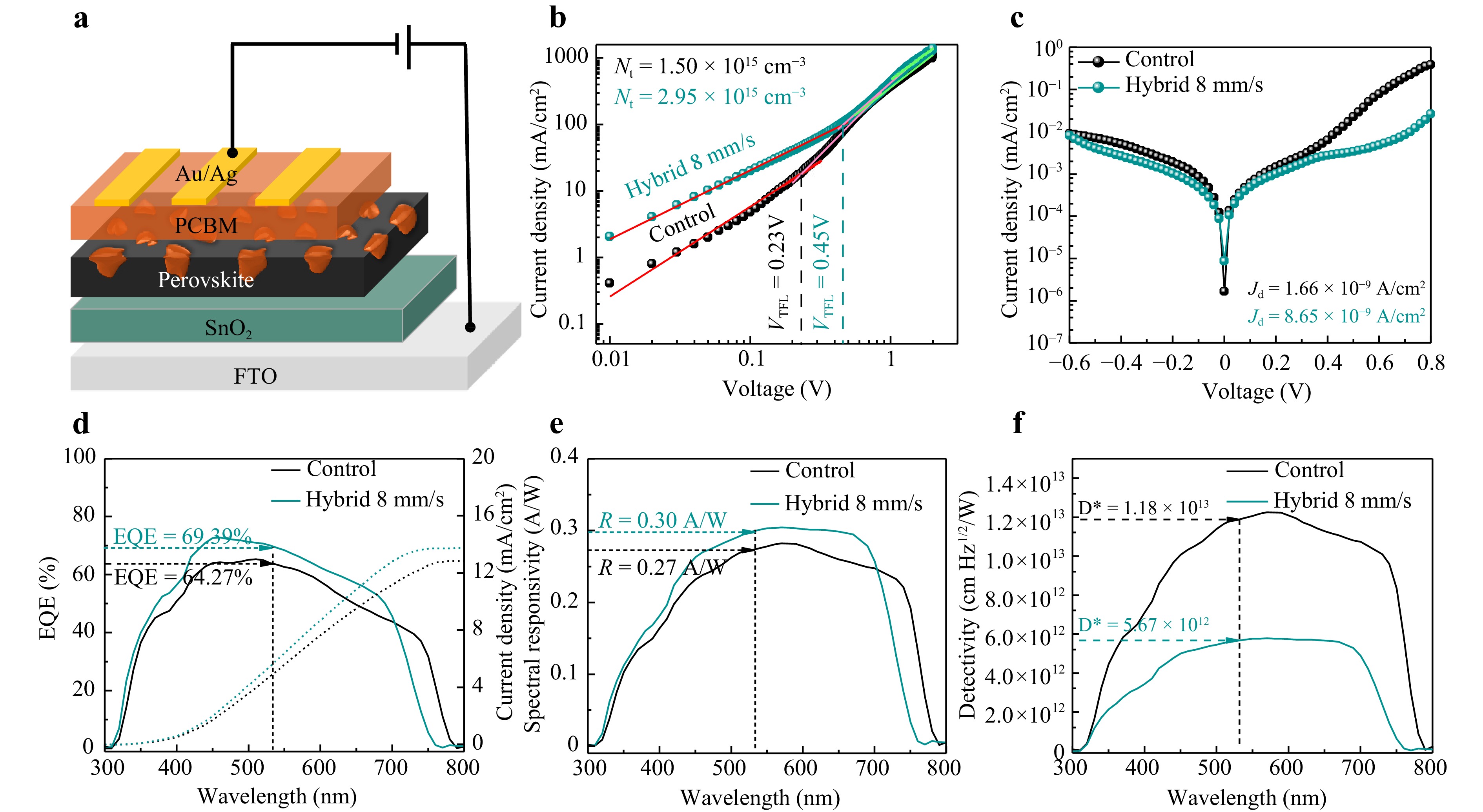
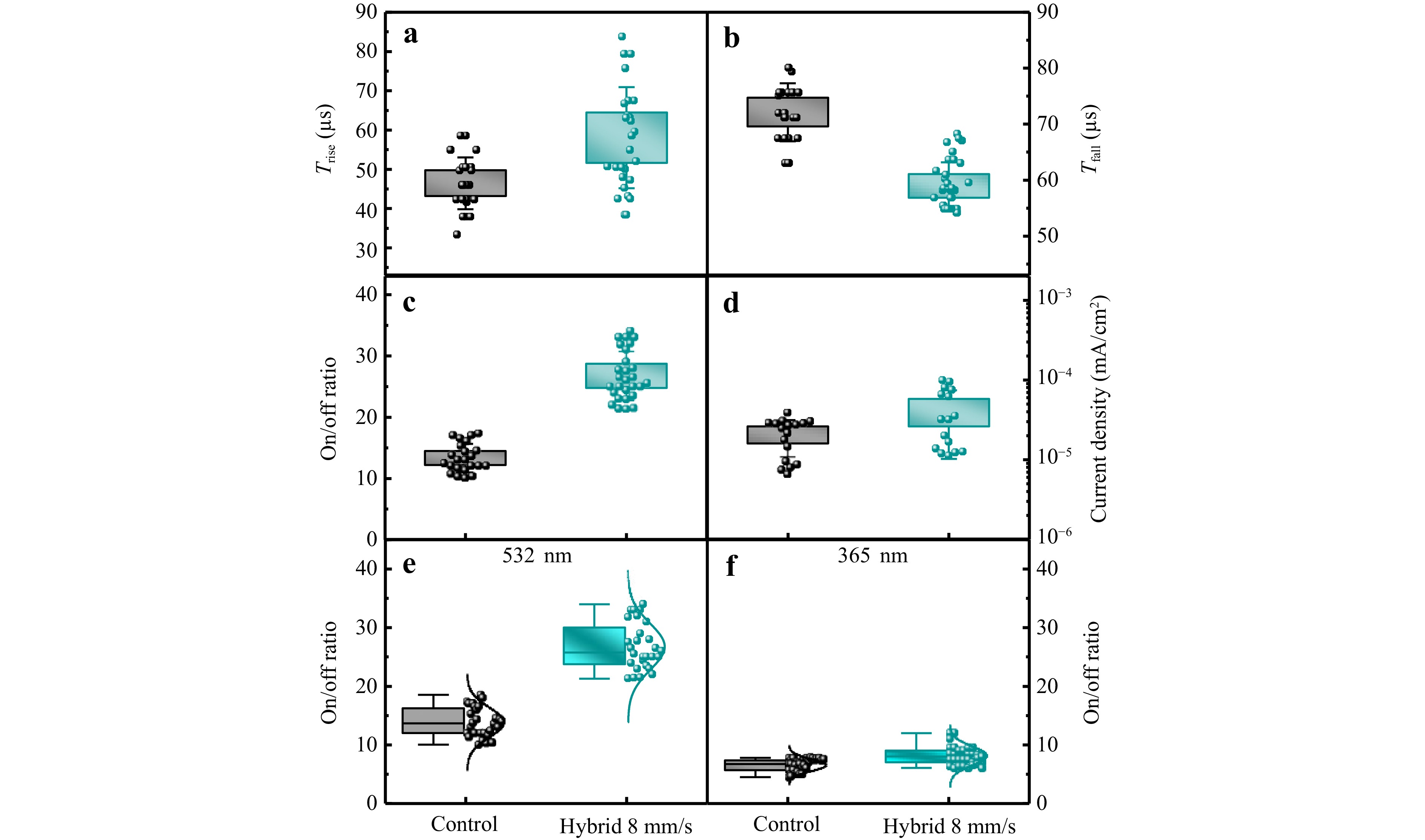
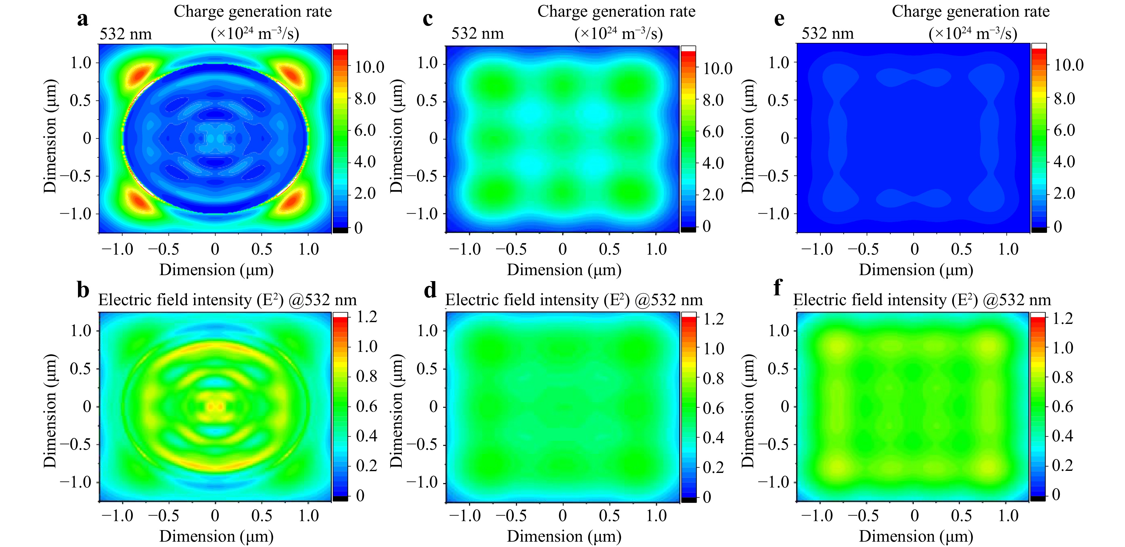
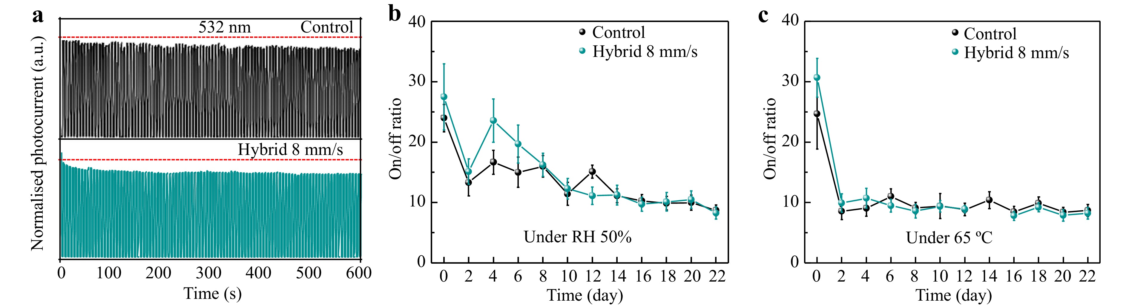
Photodetectors (PDs) are optoelectronic components that transform incident light into electrical output and are broadly applied in areas such as biomedical imaging, chemical sensing, light detection, and environmental monitoring. Although traditional PDs that use materials including Si, InGaAs, MoS2, and ZnO exhibit outstanding sensing performance, their production is expensive and complex. In contrast, perovskite-based PDs offer low-cost processability, bandgap tunability for light selectivity from the UV to IR wavelengths, and comparable detector performance. In addition, they can operate under zero-bias conditions (self-powered mode) via a photodiode configuration. In this study, we report a new hybrid perovskite-based self-powered (zero-bias) light sensor using a mixture of two perovskite materials with different band energies, exhibiting a “chocolate-chip-cookie” structure to achieve energy funnelling from one perovskite (chocolate chip) to another perovskite (cookie). By selecting CsPbBr3 as the chip and Cs0.05FA0.81MA0.14Pb (I0.85Br0.15)3 as the cookie, our device behaves like an energy-selective broadband photocurrent amplifier in self-powered mode by enhancing light detection in both the green and UV regimes (532 and 365 nm, respectively) through electric-field redistribution and energy-funnelling mechanisms. For these two wavelengths, the device achieves external quantum efficiencies of 69.39% and 47.38%, spectral responsivities of 0.30 and 0.14 A·W−1, specific detectivities of 5.67 × 10¹² and 2.65 × 1012 cm·Hz1/2·W−1, and on/off ratios of 34 and 12, respectively. Furthermore, the charge-transfer mechanism is revealed by relevant characterisations.
Published. 2026, 7(3)
: 779-789
doi: 10.37188/lam.2026.063
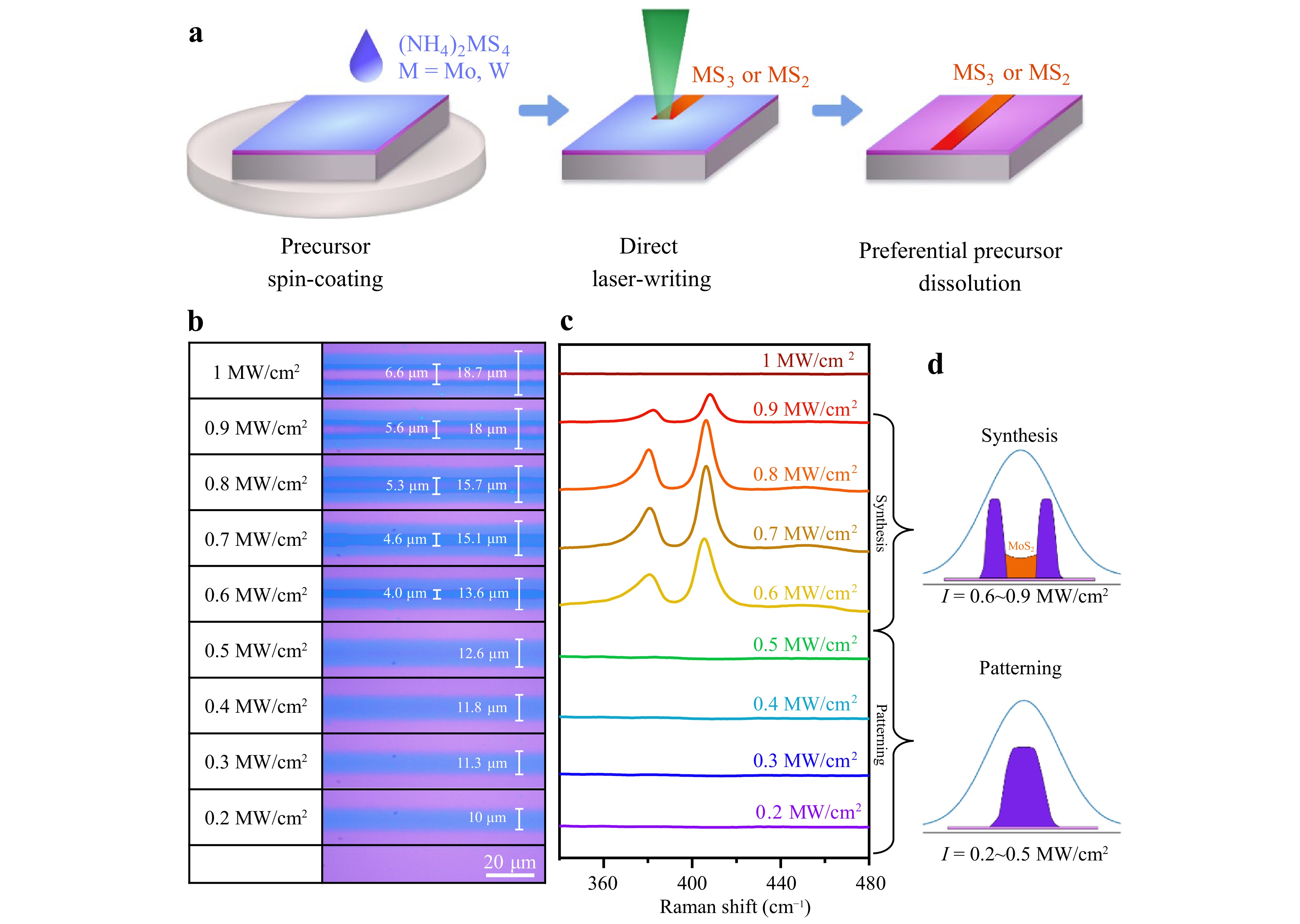
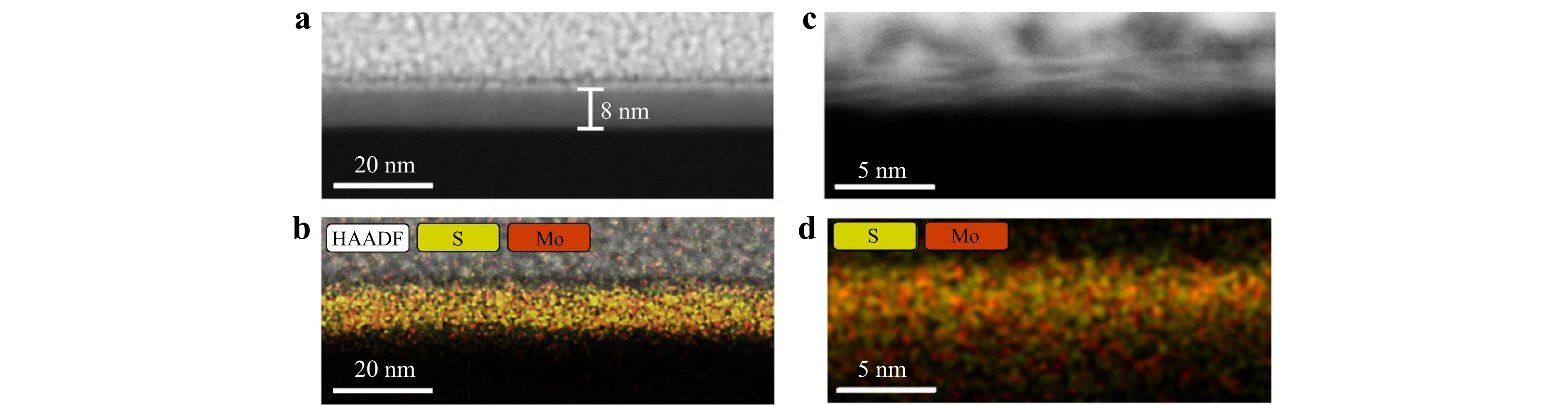
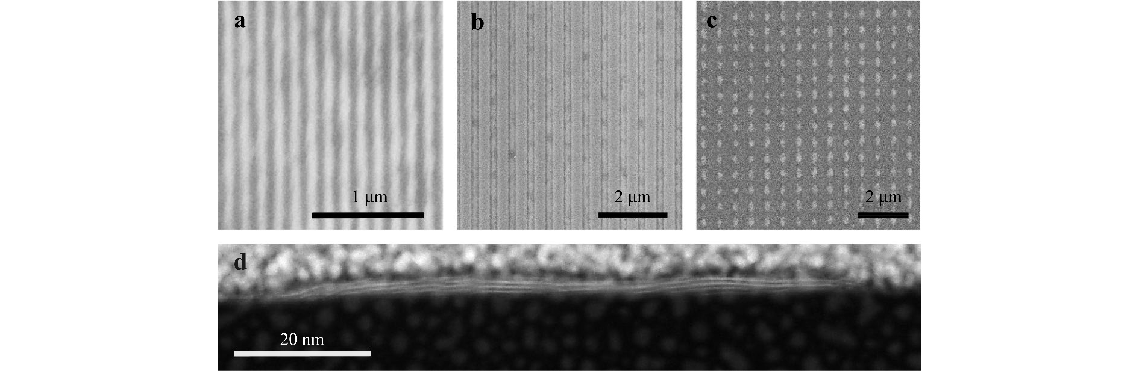
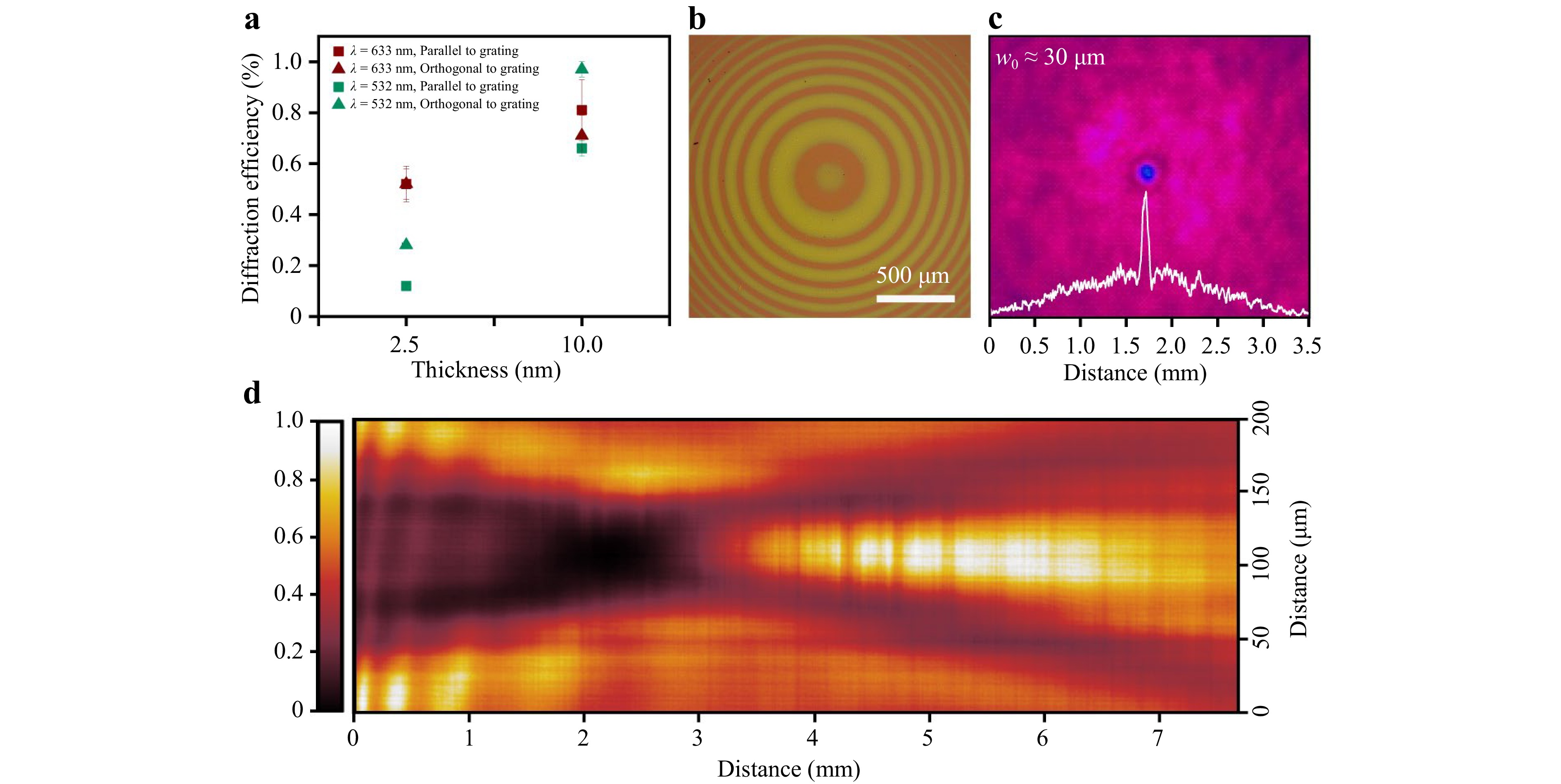
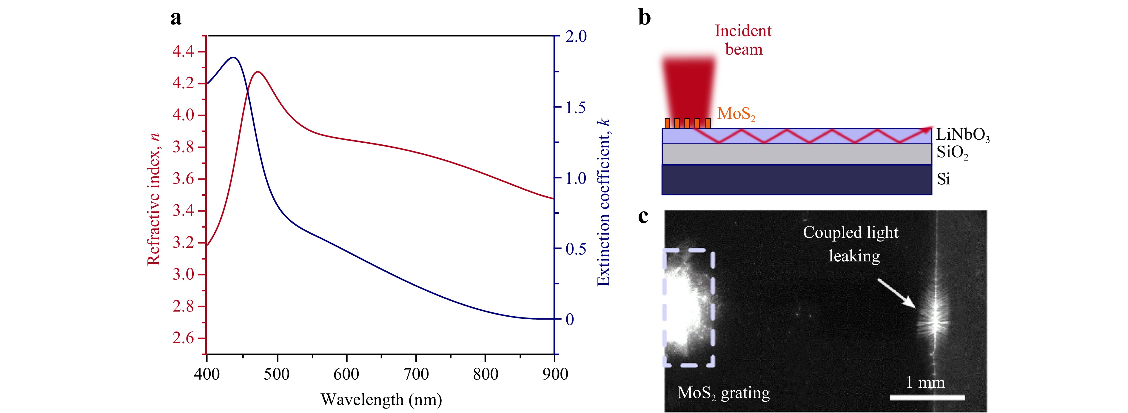
Transition metal dichalcogenides (TMDCs) are promising layered materials for nanophotonics because of their inherent optical anisotropy, large refractive indices, and optical non-linearity, which make them excellent candidates for integration into photonic components. However, current prototyping techniques used to fabricate functional photonic elements rely on post-processing of single-crystal flakes or chemical vapour deposition (CVD)-grown films via focused ion beam milling, which is a throughput-limited and time-consuming approach. Therefore, scalable and rapid patterning methods for TMDC-based photonic devices are required to boost their application in the field of photonic technologies. Herein, we present a laser lithography method that enables the direct production of ultrafine diffractive MoS2 and WS2 structures from their chemical precursors. Thin films of thiosalt precursors, spin-coated onto various substrates, can be patterned with high resolution when exposed to light in the visible and ultraviolet (UV) spectral regions in a photolithographic manner. This allows either the direct synthesis of TMDC structures or the production of micro/nanopatterns consisting of partially synthesised amorphous material from the initial precursor films, which can later be converted to the desired TMDC using a two-step process. Using interferometric lithography, we fabricated of MoS2 and WS2 diffraction gratings with periods as short as 150 nm and aspect ratios ~104 (length/width), as well as MoS2 Fresnel holograms on photonic substrates such as silica (SiO2) and lithium niobate (LiNbO3). An MoS2 grating coupler was fabricated and used to couple light onto a thin-film lithium niobate planar waveguide. The measured diffraction efficiencies of the laser-patterned multi-layer MoS2 gratings at visible wavelengths matched the corresponding values reported for exfoliated TMDC materials, highlighting the potential of this method for fabrication of 2D photonics.
Published. 2026, 7(3)
: 790-802
doi: 10.37188/lam.2026.020
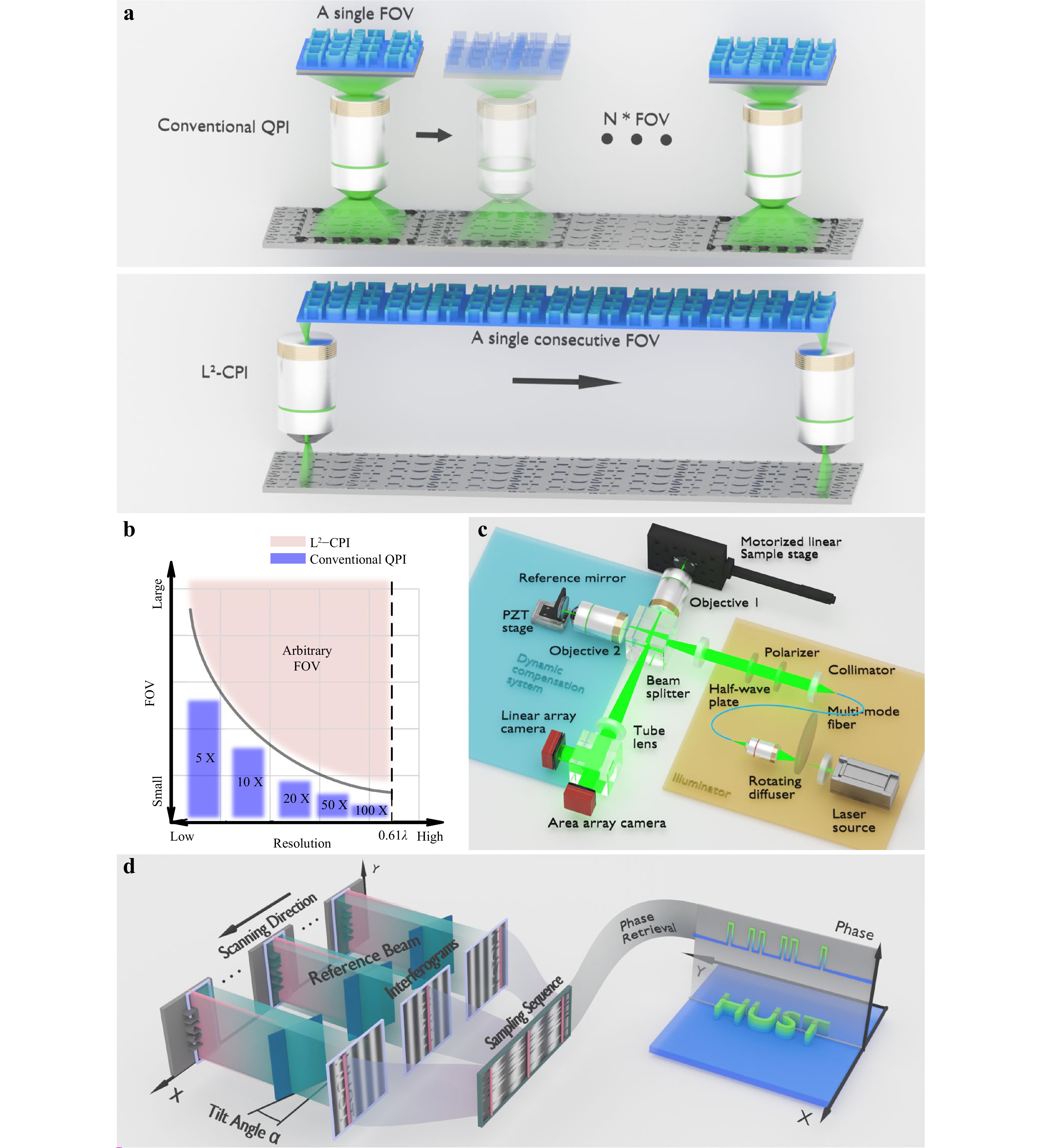
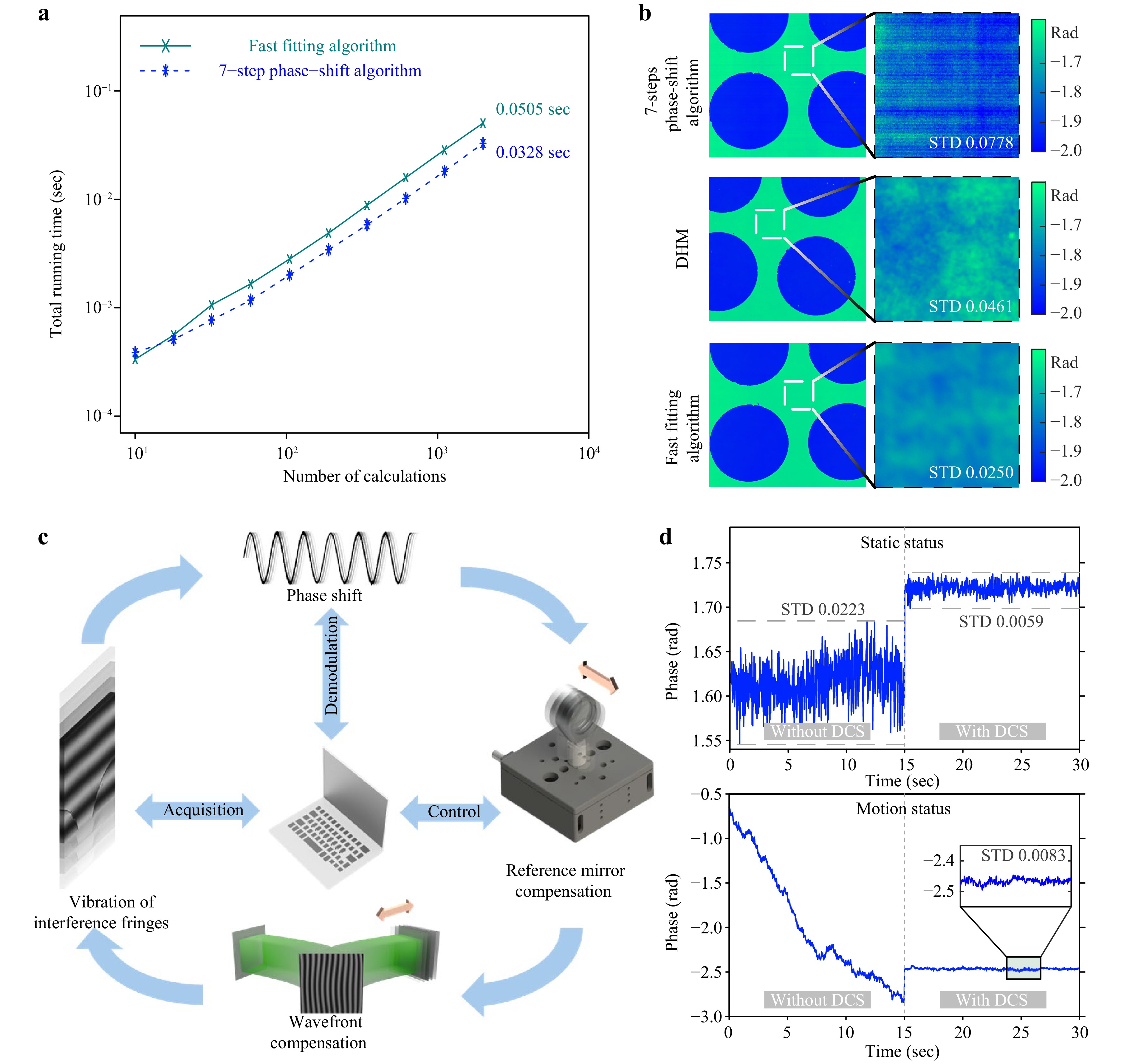
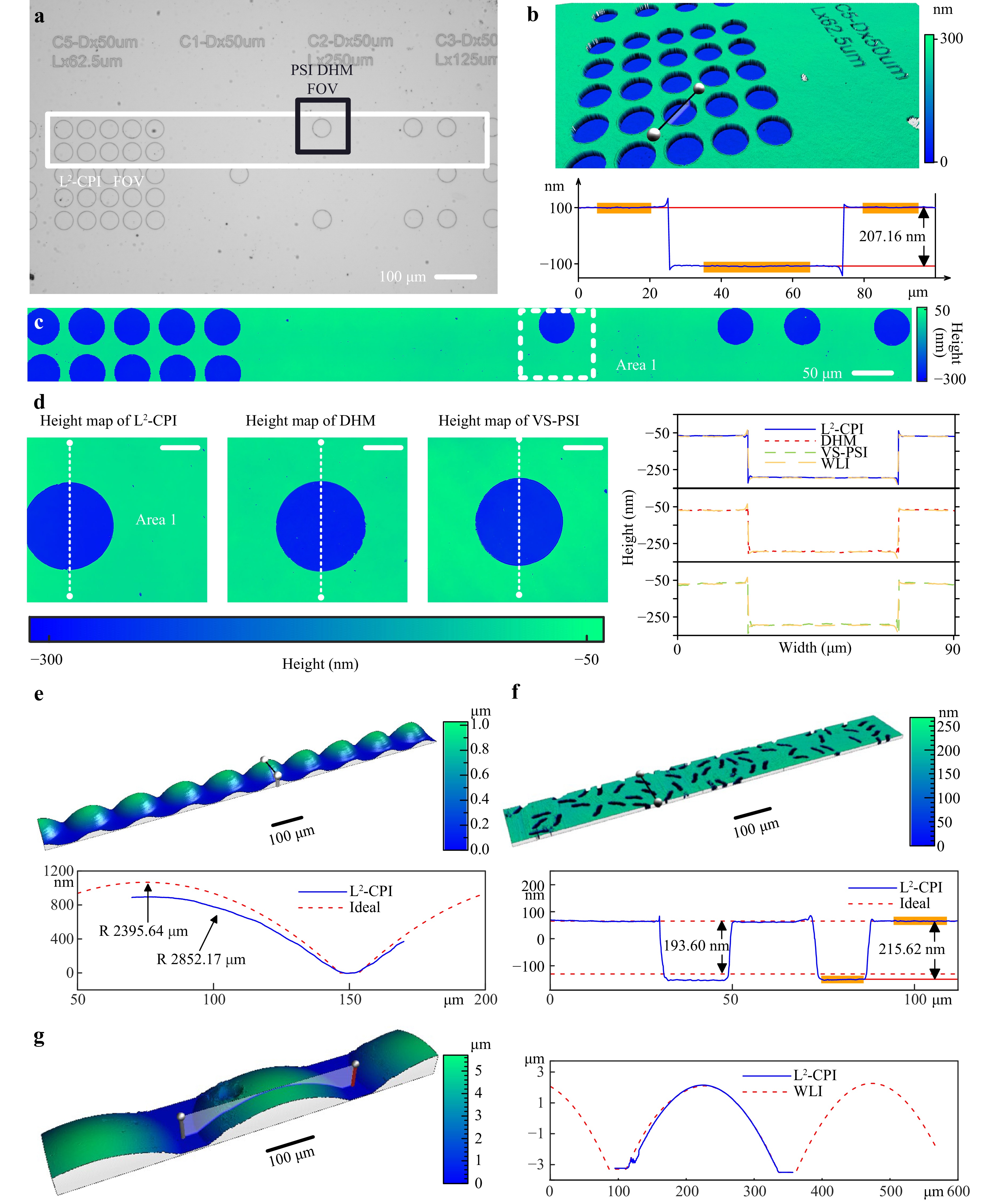
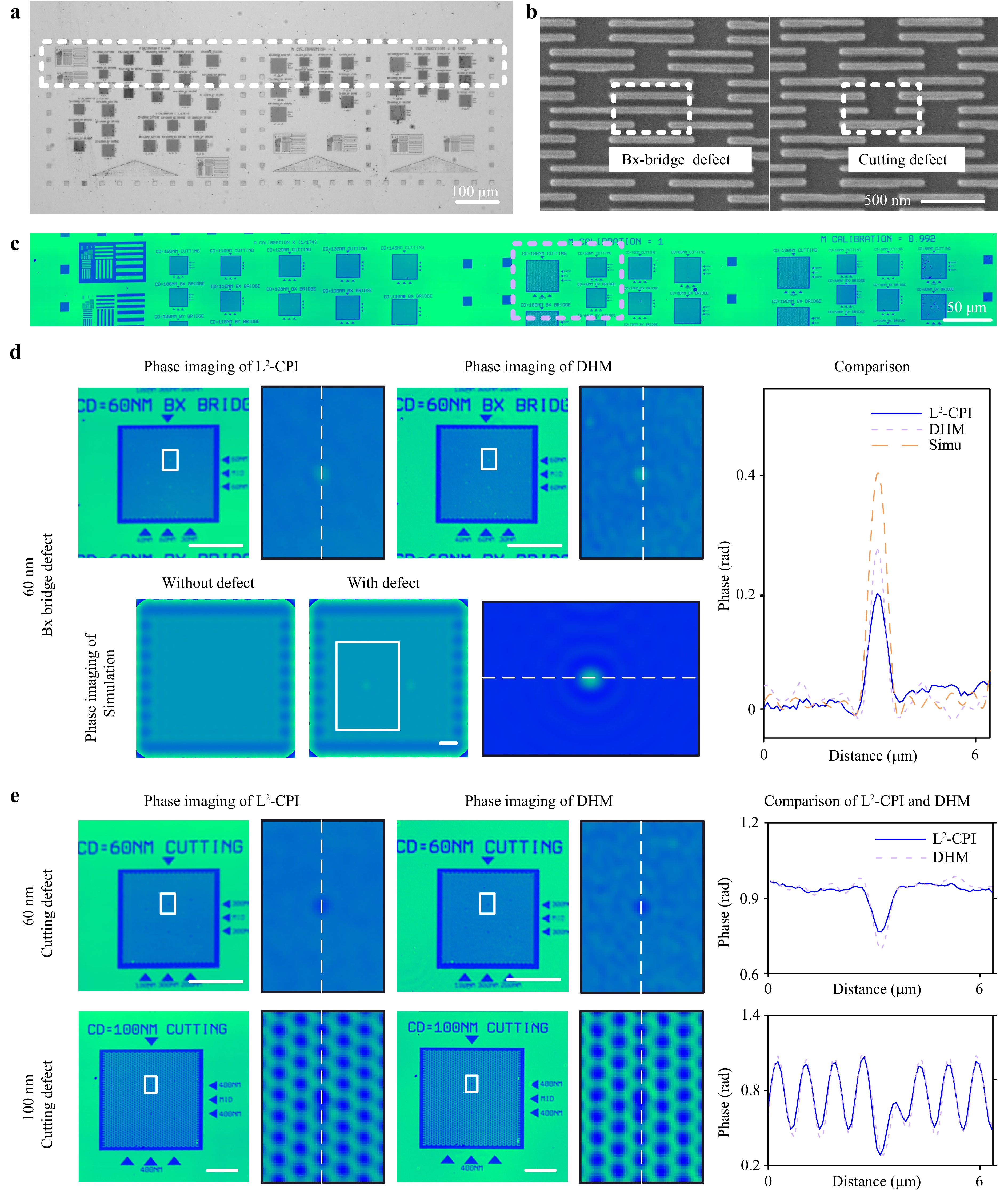
Optical phase imaging is a powerful tool widely used in bioimaging, material characterization, pathology, and nanomanufacturing. Yet, it faces a persistent challenge: the inherent contradiction between resolution and field of view (FOV) in conventional microscope-based systems. To address this limitation, we propose Lateral Line-Scan Computational Phase Imaging (L2-CPI), a novel computational phase imaging architecture that enables consecutive phase imaging of moving samples. Our experiments with both transparent and opaque samples demonstrate that L2-CPI achieves an equivalent FOV of D × L, where D is the camera sensor edge length and L is the motorized stage travel range. This implies that the equivalent FOV of L2-CPI in a single measurement can be arbitrarily large, provided the stage travel range L is arbitrarily long. Our work breaks the long-term contradiction between resolution and FOV, establishing a new paradigm for ultra-large-FOV phase imaging in dynamic mode without sacrificing optical resolution. This advancement holds significant potential for applications in bioimaging, material characterization, biosensing, nanometrology, and semiconductor inspection.
Published. 2026, 7(3)
: 803-813
doi: 10.37188/lam.2026.066
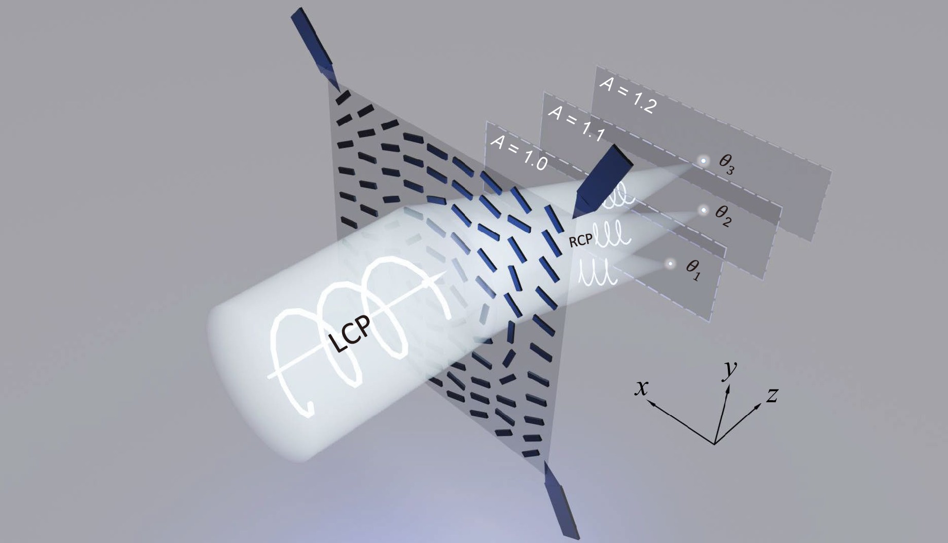
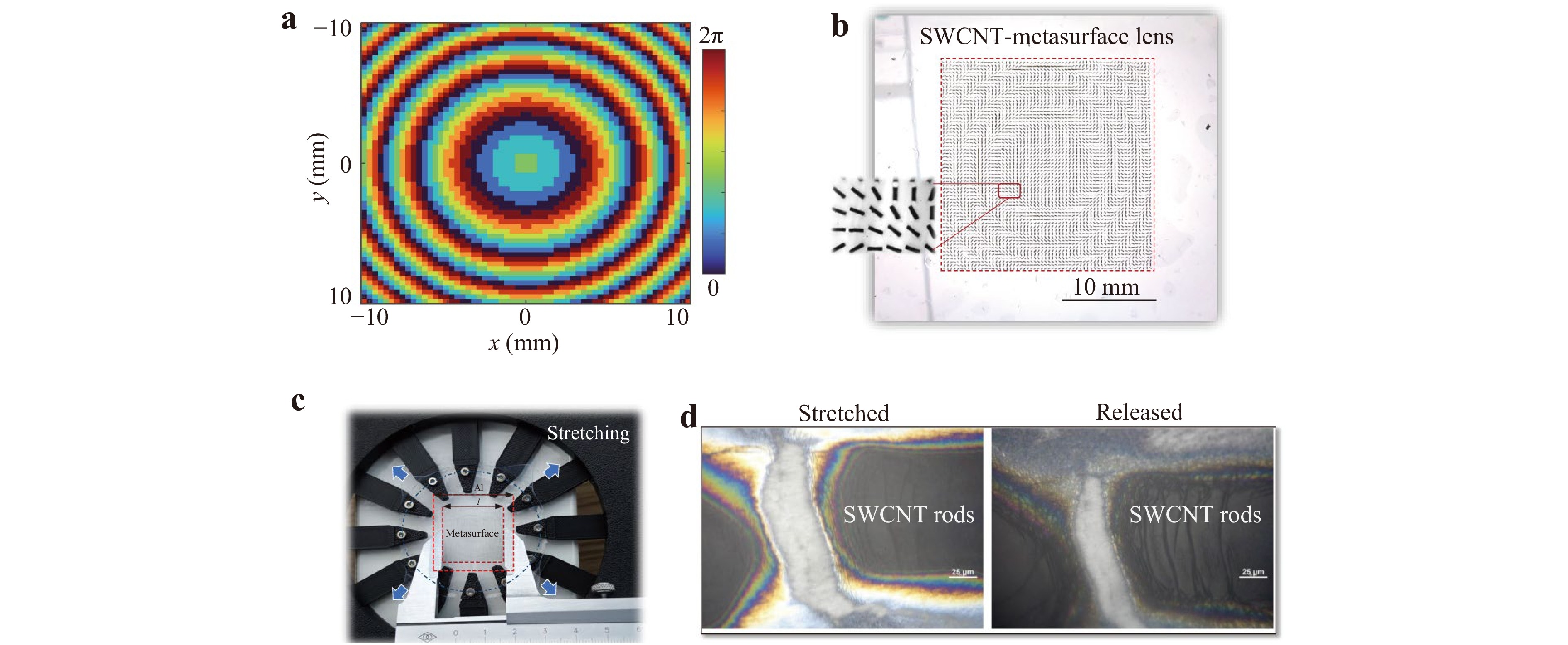
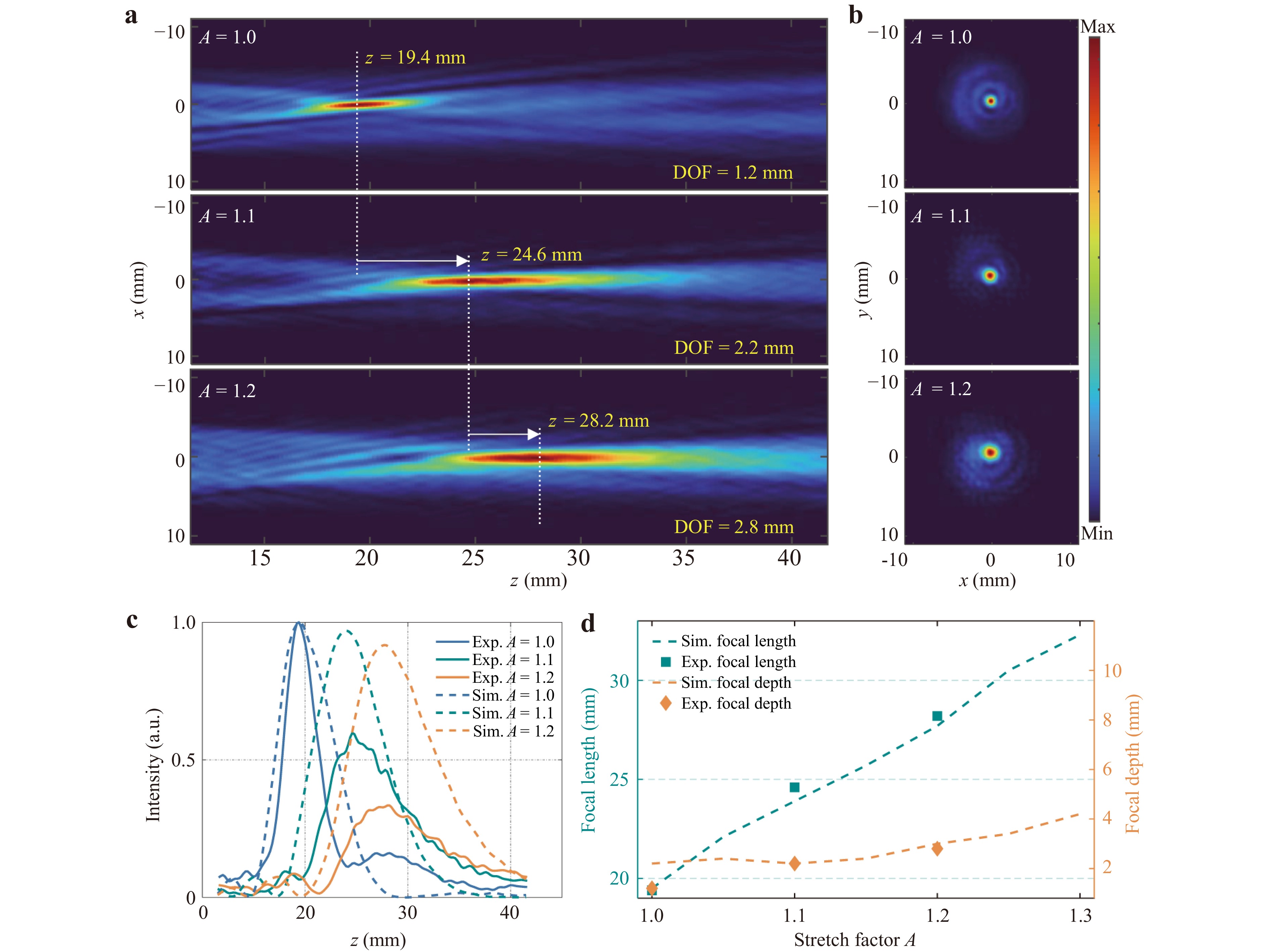
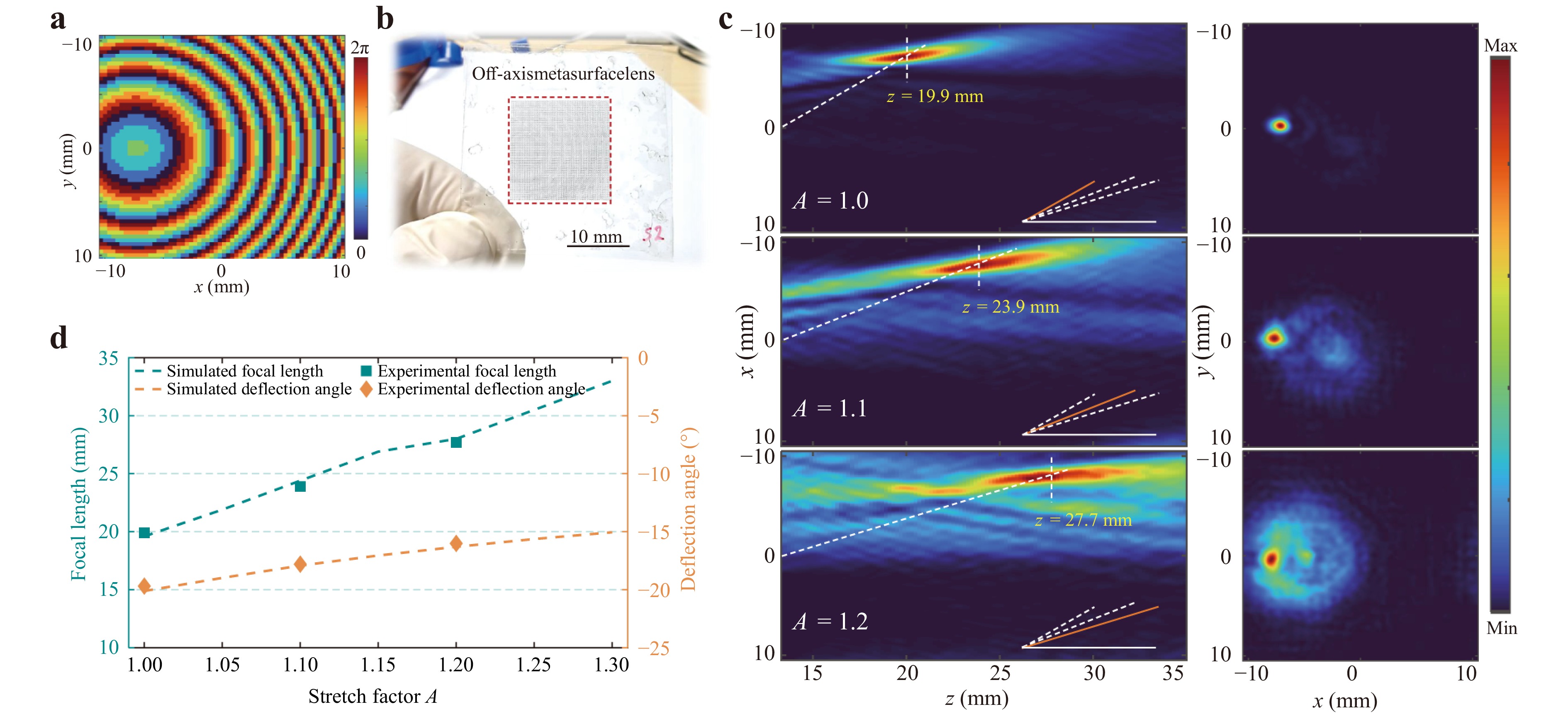
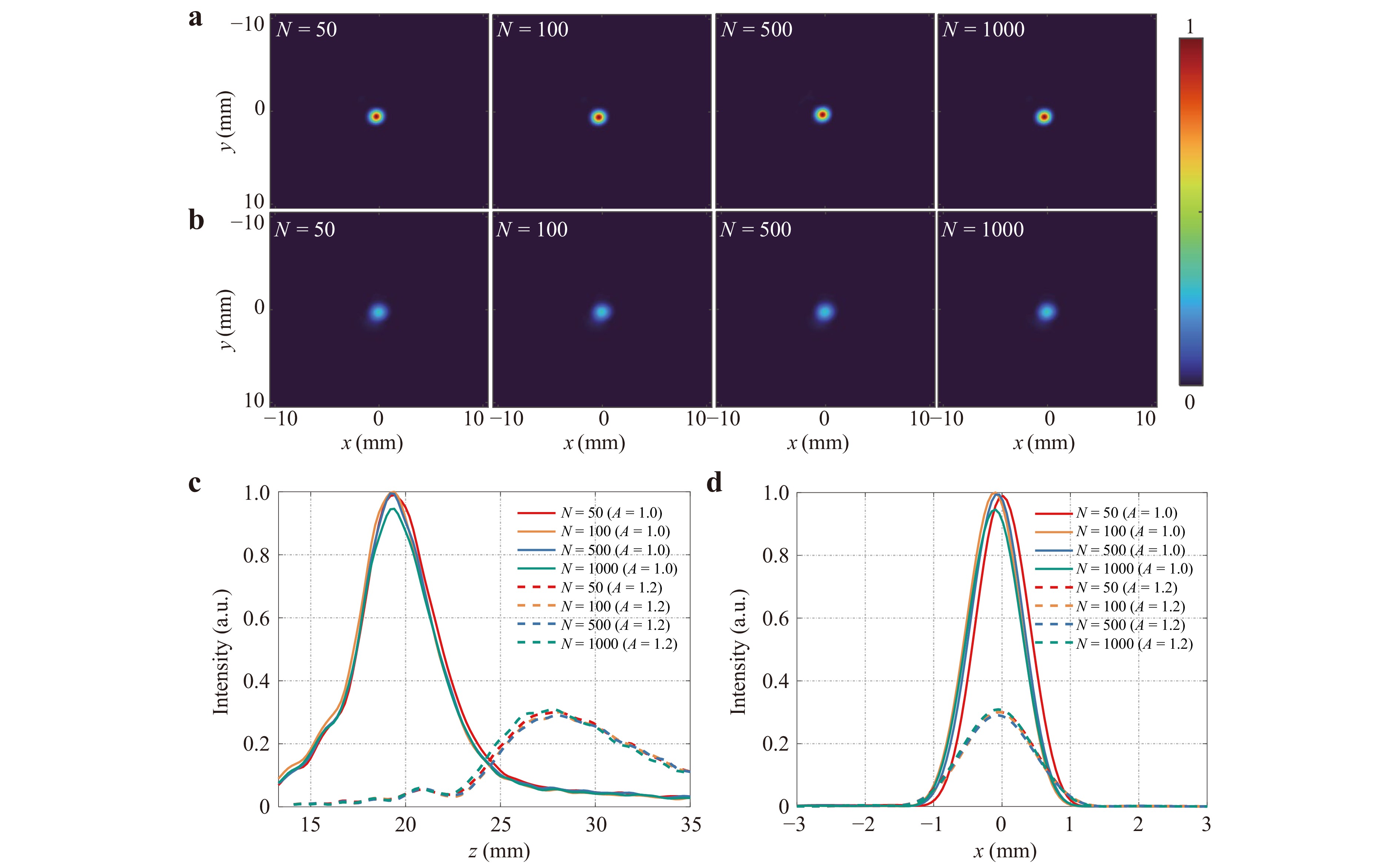
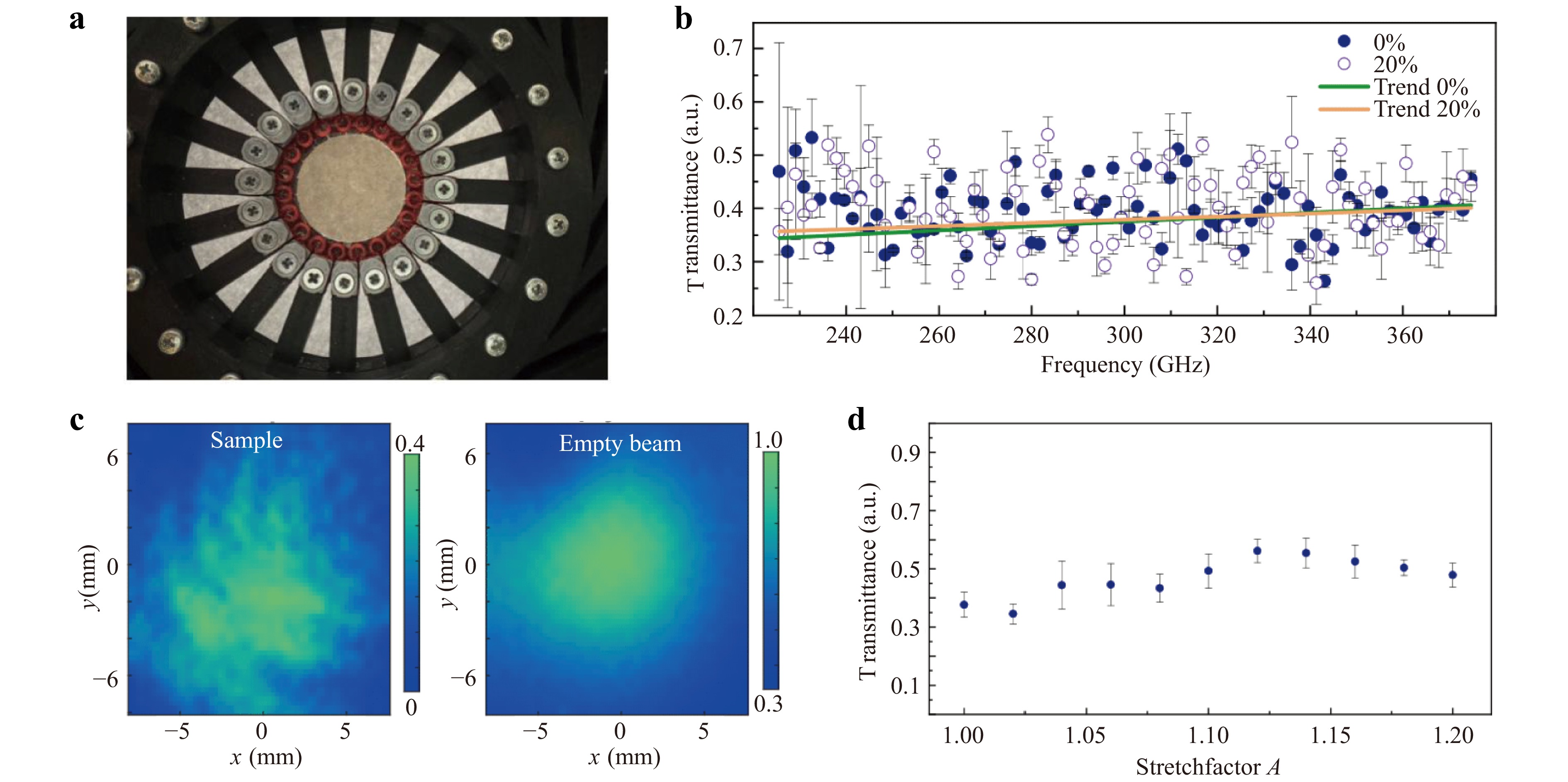
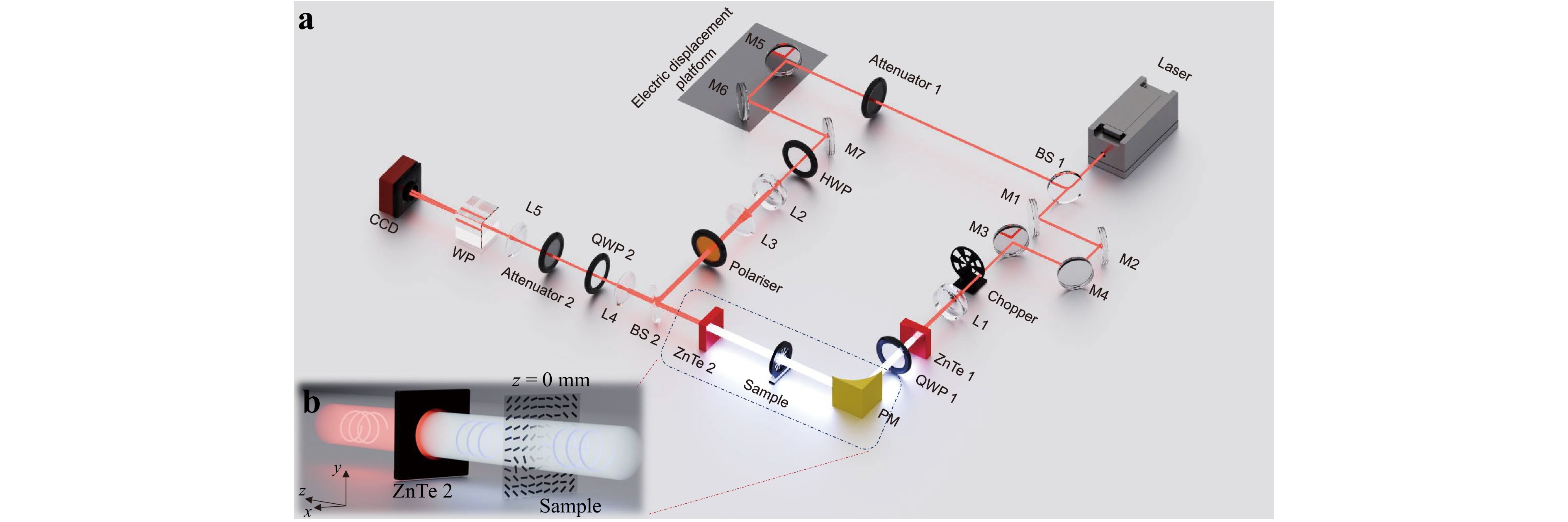
The terahertz (THz) technology has a pivotal role in advancing next-generation communication systems, offering distinctive advantages for high-speed data transmission and precise sensing. Concurrently, flexible functional devices have emerged as a key research focus due to their ability to conform to complex application scenarios through mechanical deformation. The integration of THz wavefront manipulation with flexible platforms is crucial for unlocking innovative applications. However, existing devices often lack the dynamic tunability required for practical implementation. Here, we demonstrate two types of flexible THz metasurfaces for phase modulation based on the Pancharatnam-Berry phase modulation, operating at 0.35 THz. Each device comprises an array of single-walled carbon nanotube resonators on a silicone substrate. The first design is a mechanically tuneable metasurface lens. Under a stretch factor of A = 1.2, the focal spot shifts rearwards, and the focal length increases from 19.4 to 28.2 mm (an increment of 8.8 mm). The second design enables dynamic beam deflection through controlled mechanical stretching. At the same stretch factor (A = 1.2), the deflection angle varies from −19.69° to −16.01°, with a change of 3.68°. These results provide a viable technical pathway for dynamic THz wavefront modulation, laying a solid foundation to enhance THz applications in future communication systems and expand the potential of flexible devices in high-frequency electromagnetic fields.
Published. 2026, 7(3)
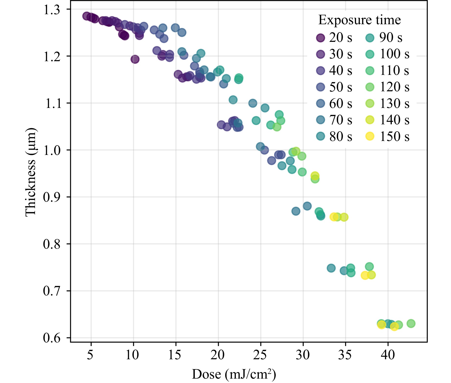
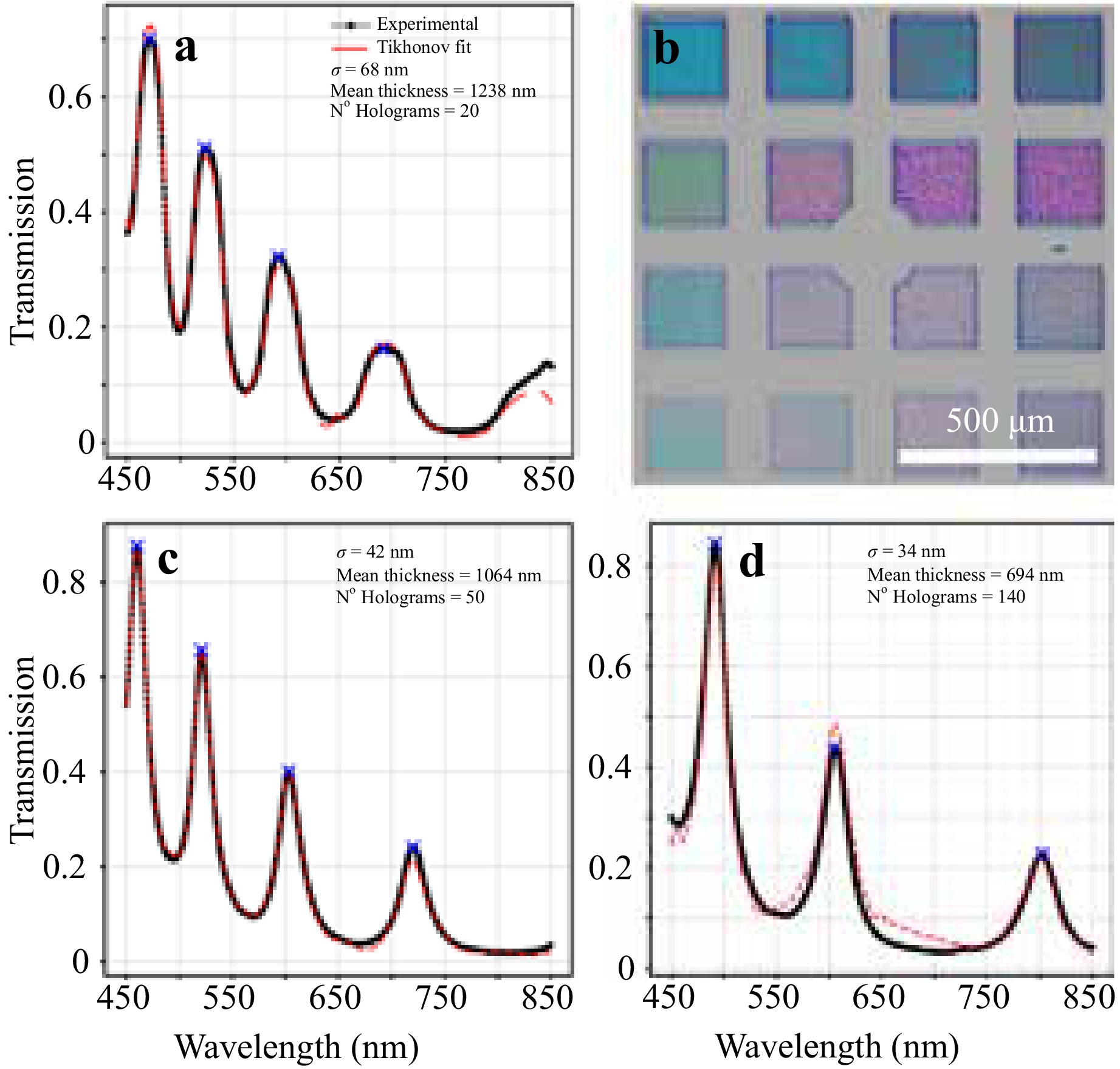
: 814-822
doi: 10.37188/lam.2026.076
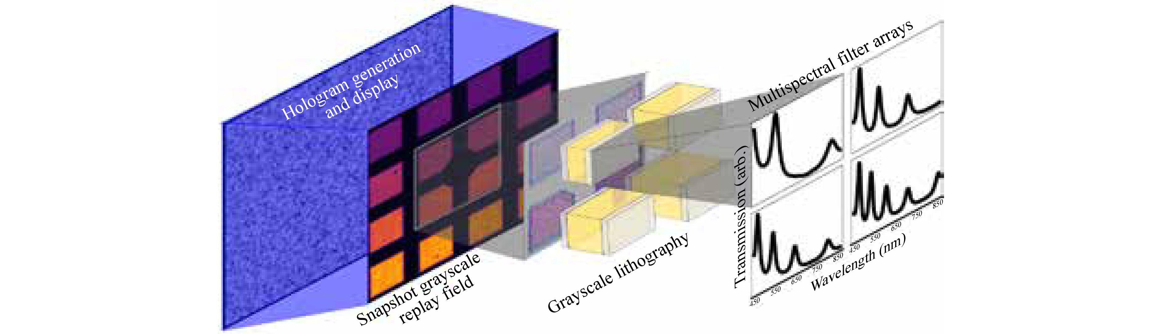
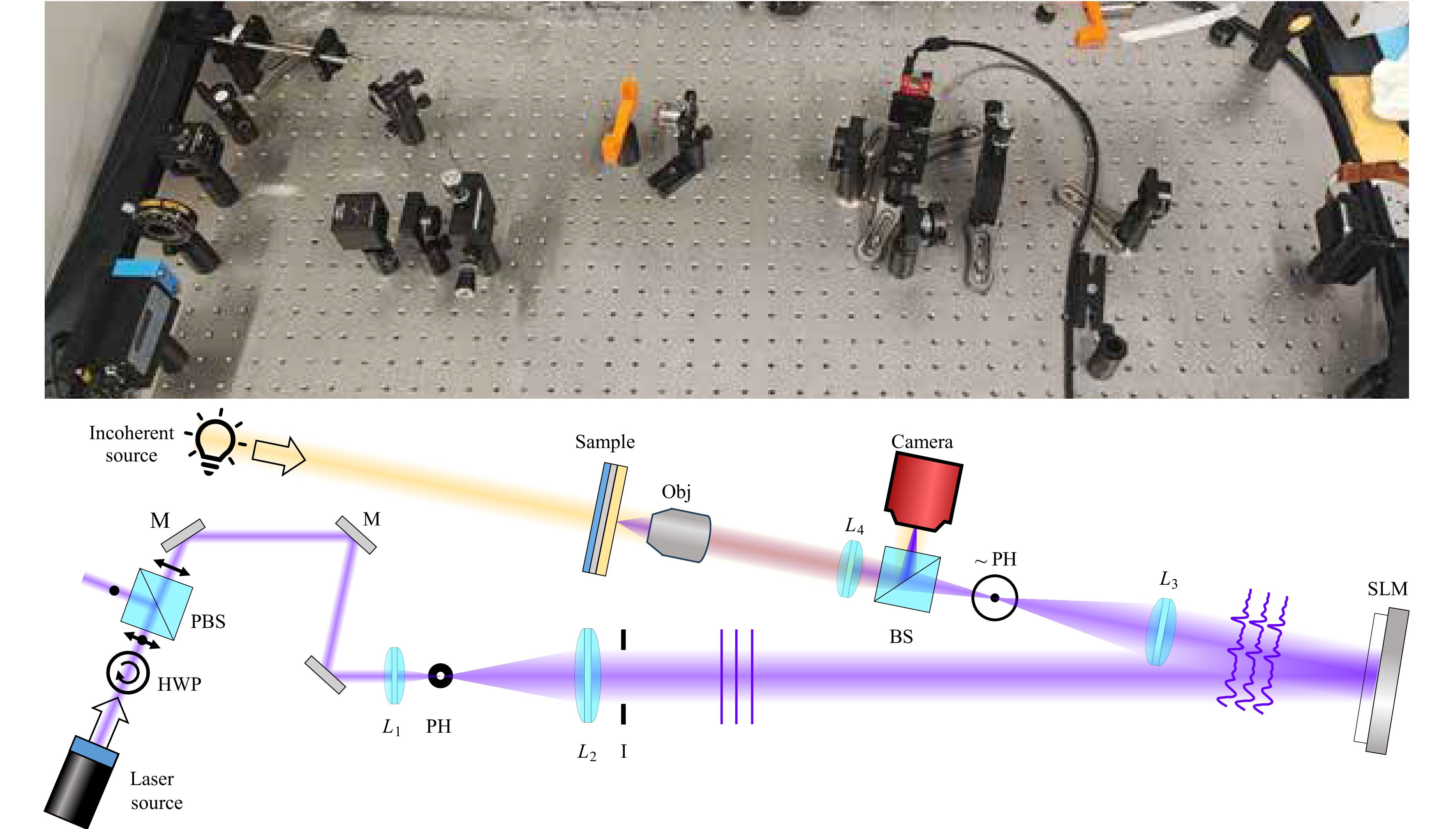
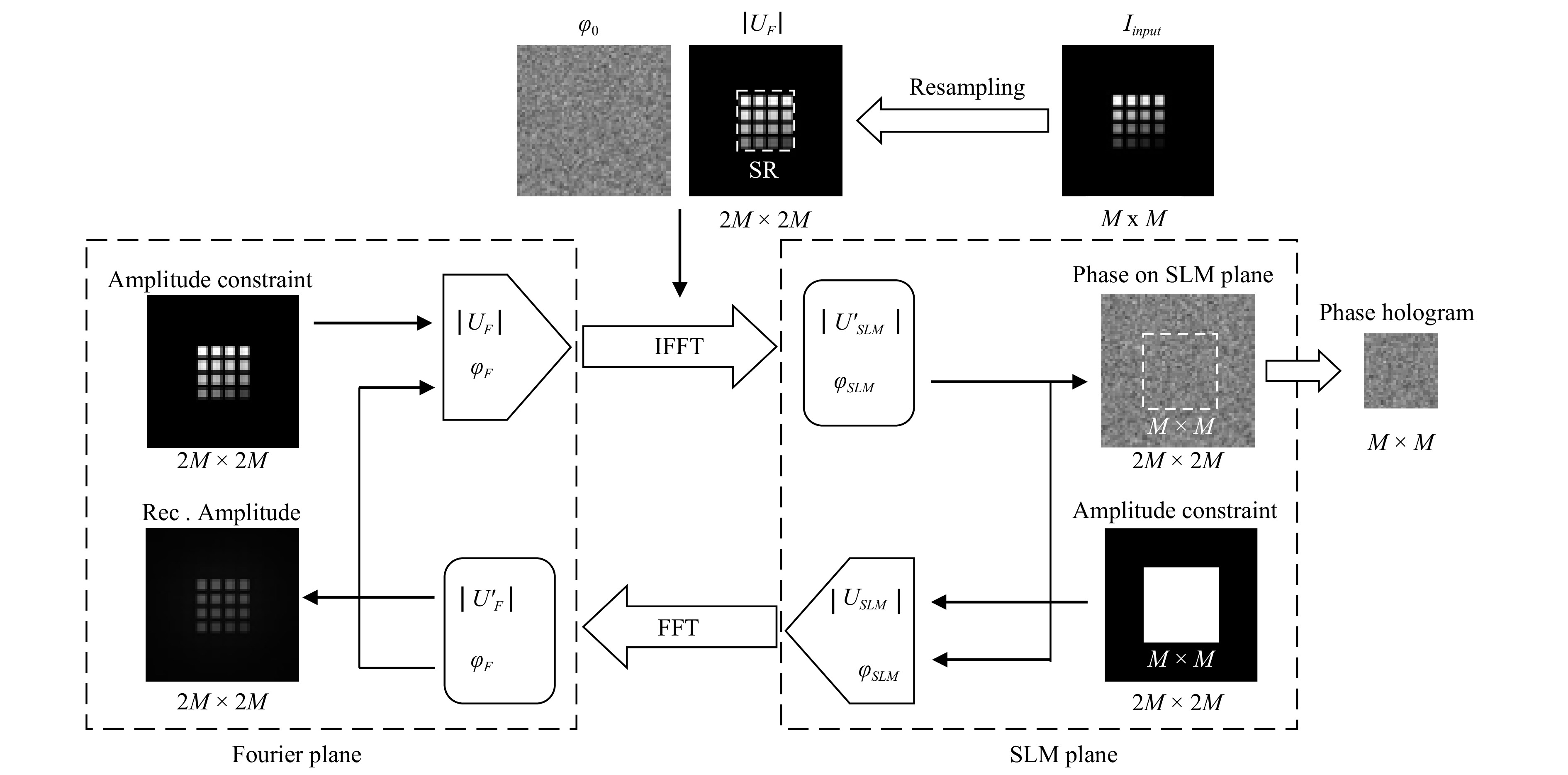
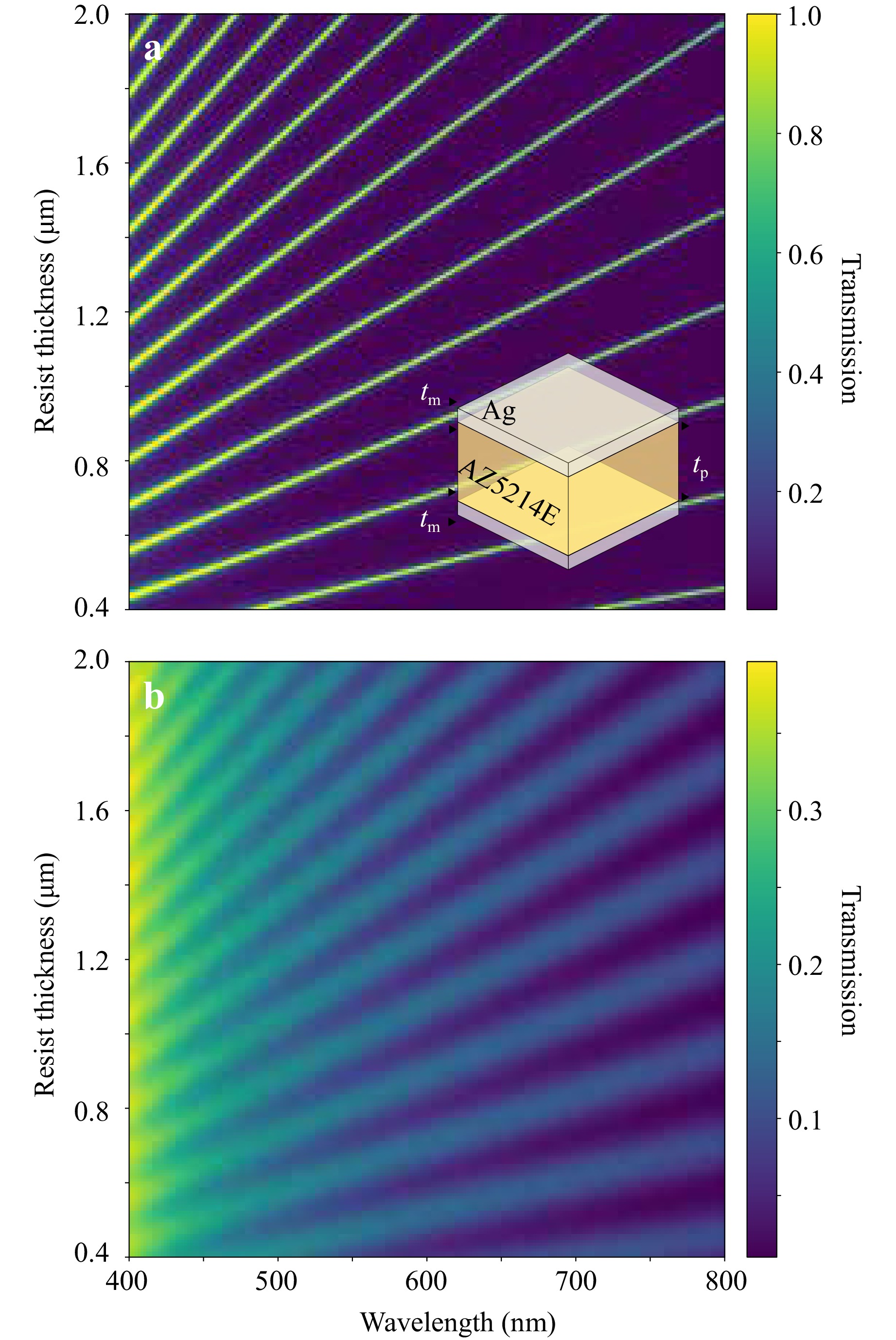
Multispectral filter arrays underpin compact spectral imaging but are typically fabricated through complex multistep photolithography. Herein, we demonstrate a single-step holographic grayscale lithography method that uses a spatial light modulator to directly write Fabry-Perot filter arrays. A phase-retrieval algorithm is used to compute holograms that project grayscale intensity patterns onto a photoresist, enabling cavity thicknesses ranging from 600 to 1,300 nm across a single exposure. In this study, transmission spectra were modelled using transfer-matrix simulations with Monte Carlo averaging to capture thickness variations, and experimental spectra were fitted via Tikhonov-regularized inversion. Good agreement was observed between the theory and experiment (R2 \begin{document}$\approx$\end{document}
Published. 2026, 7(3)
: 823-834
doi: 10.37188/lam.2026.080
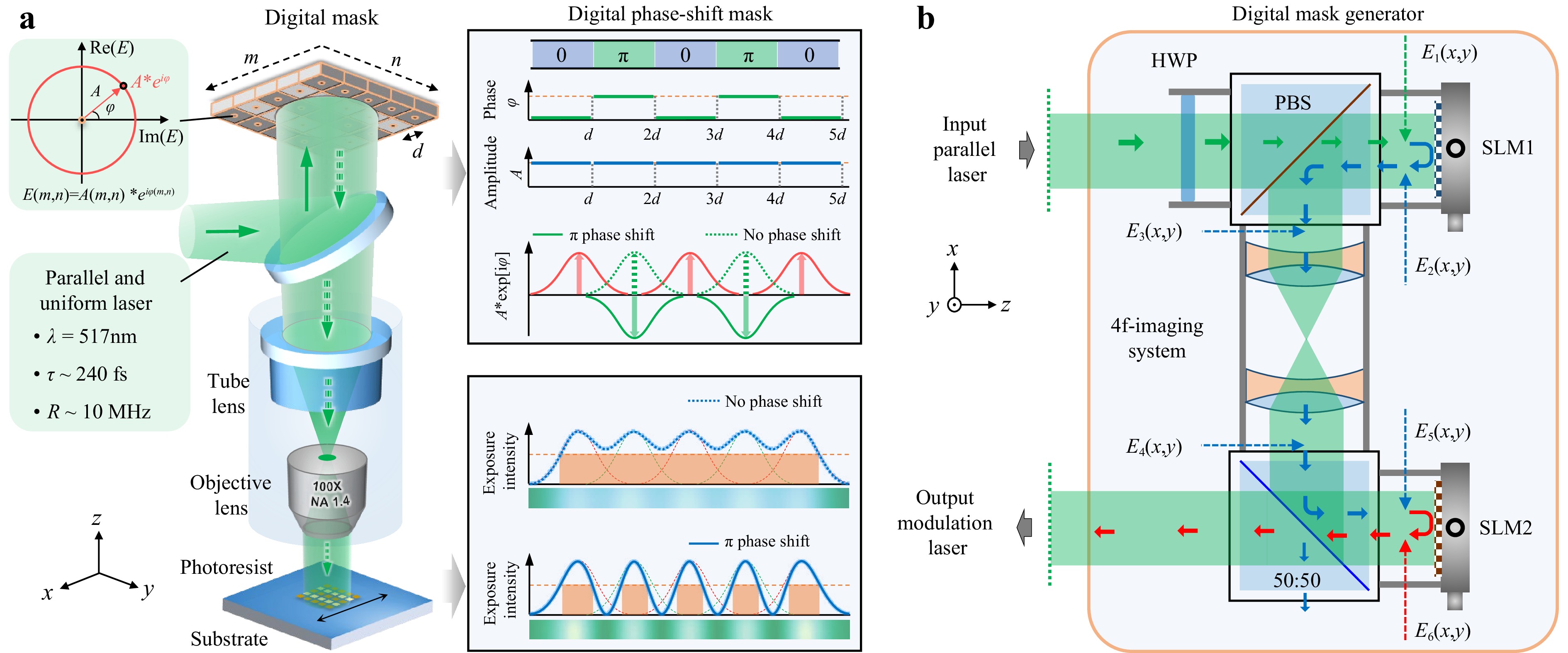
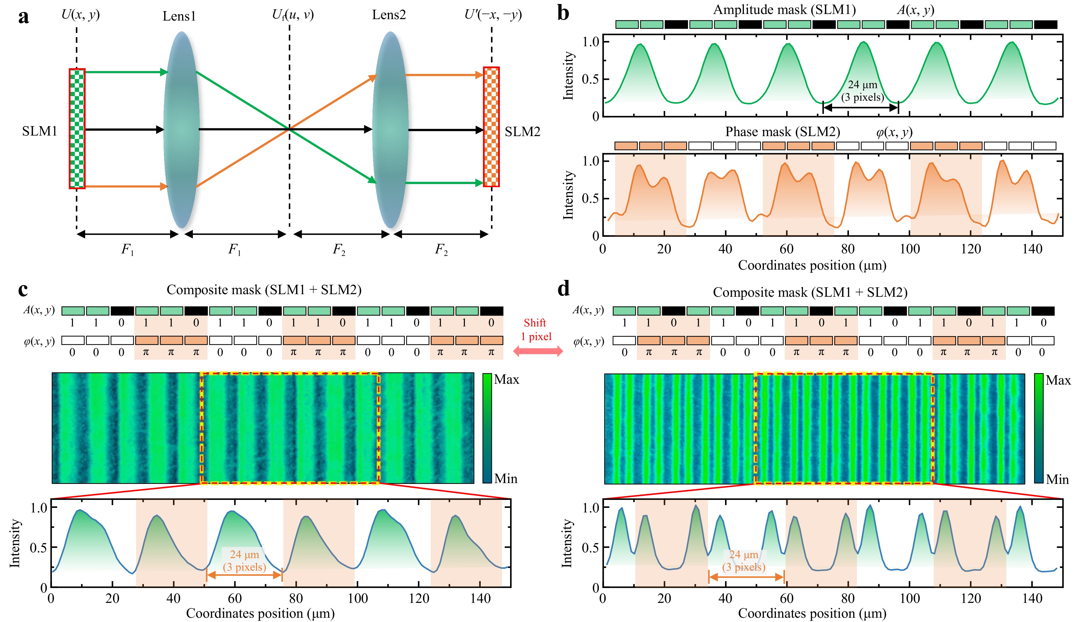
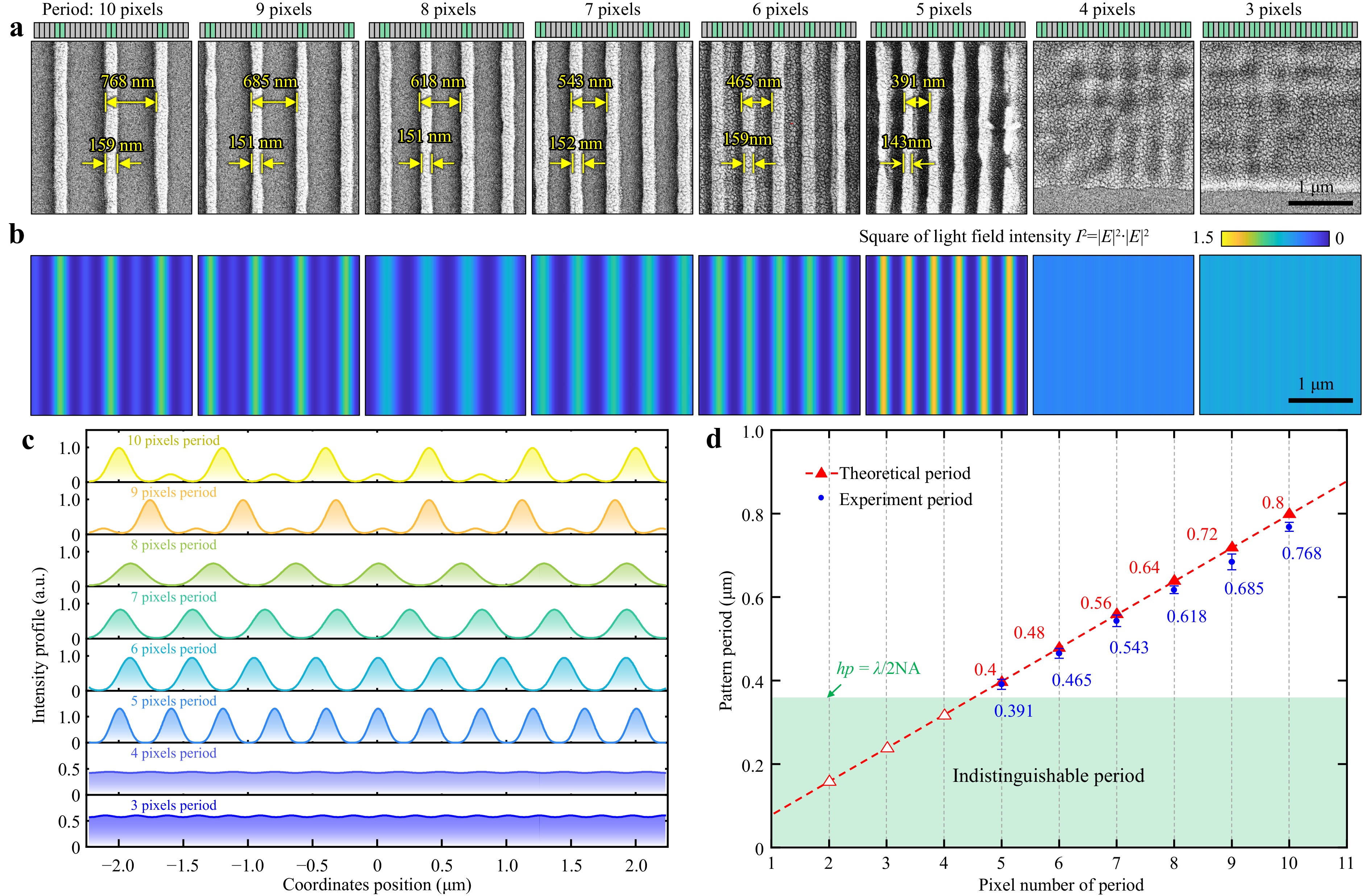
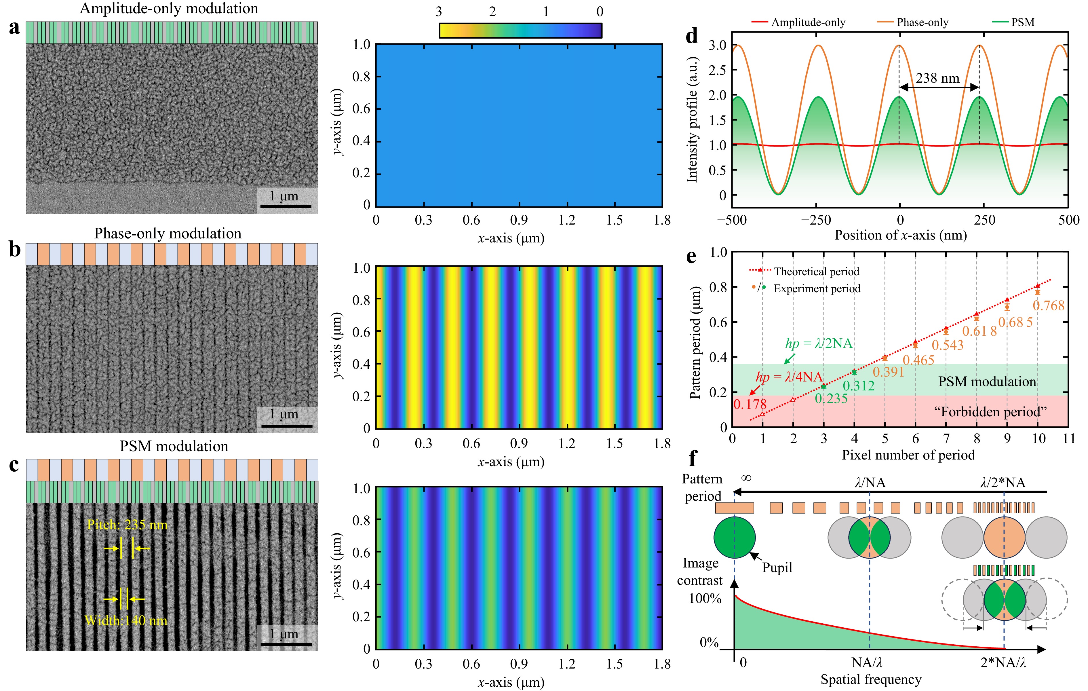
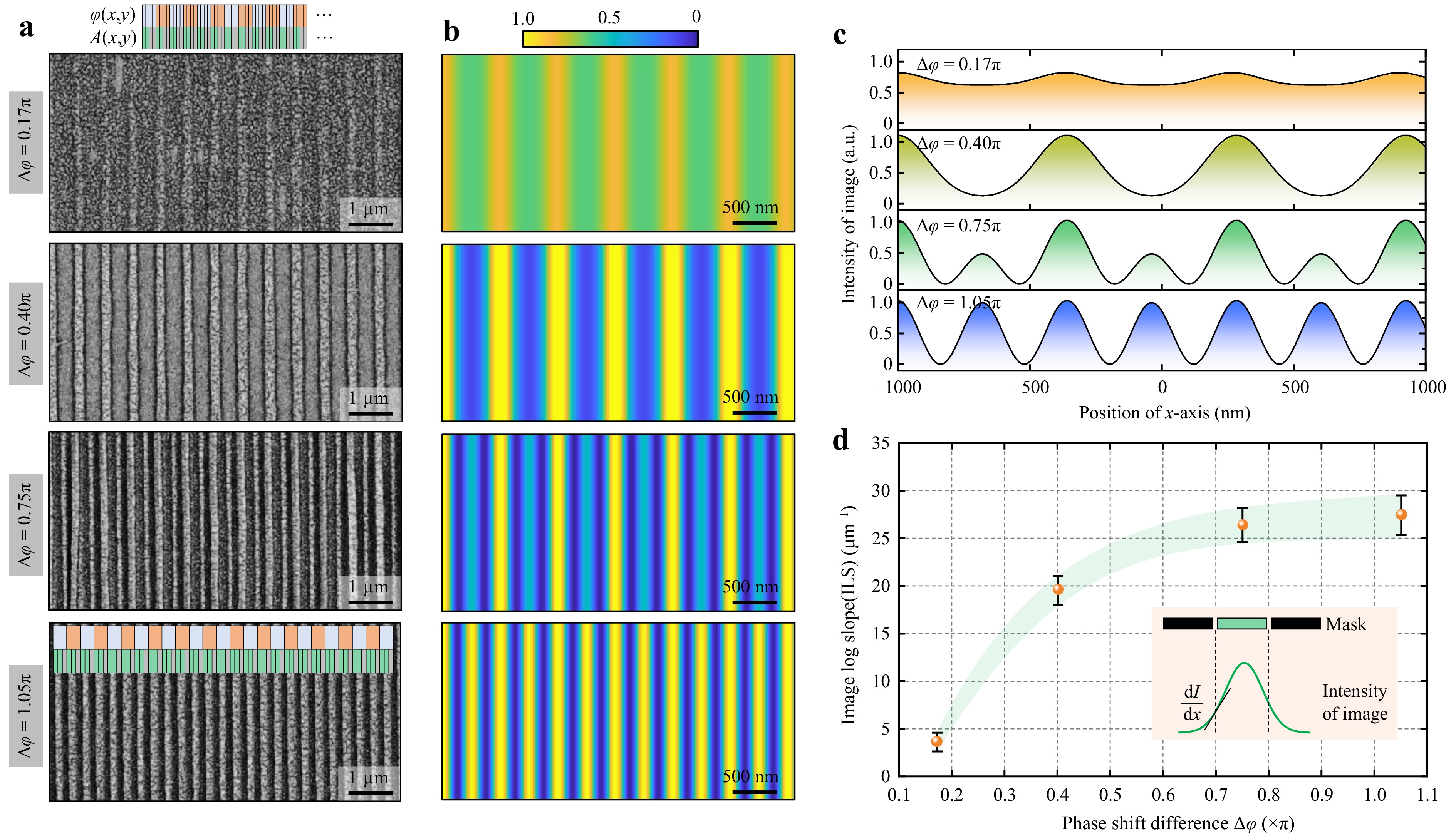
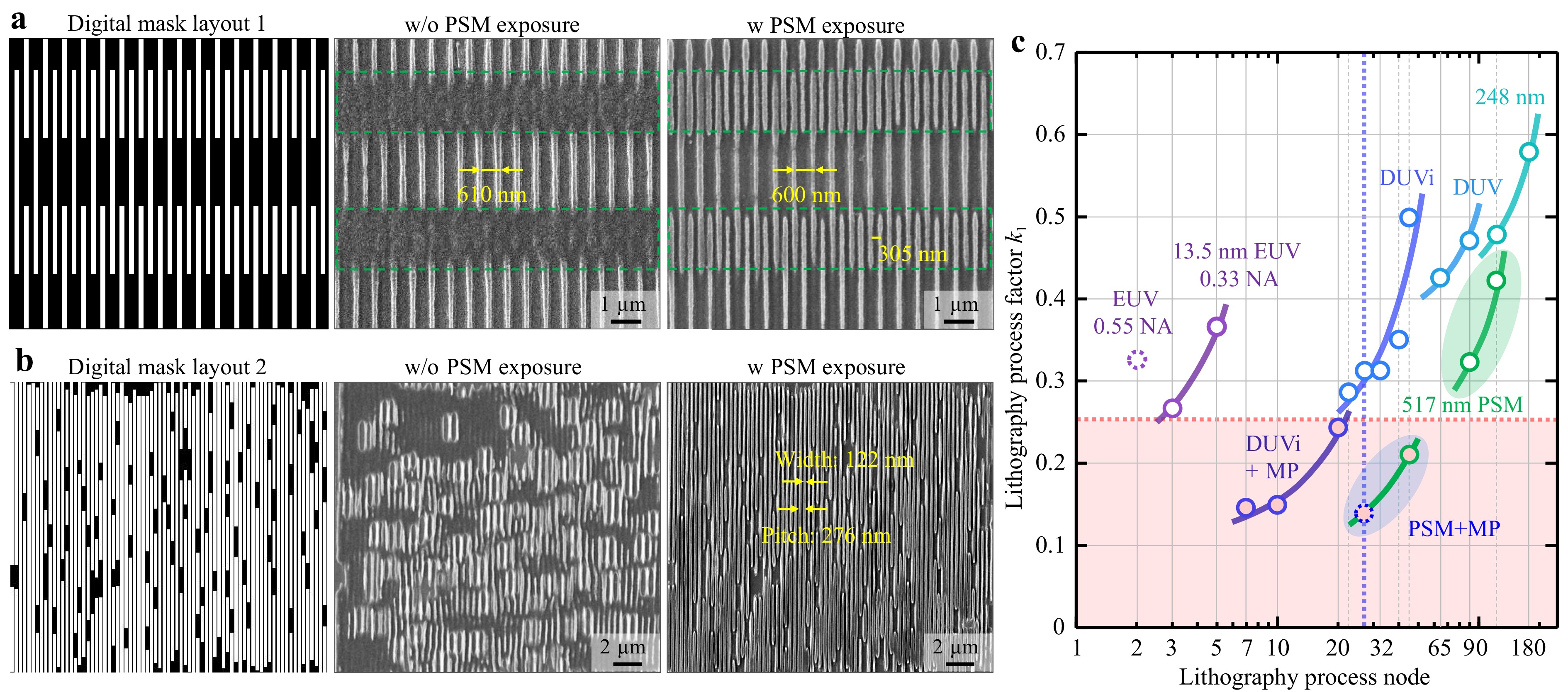
The diffraction limit poses a fundamental challenge to digital mask projection lithography (DMPL) in fabricating subwavelength-scale dense periodic patterns, limiting its application in advanced chip manufacturing. To address this, we present a DMPL platform with a resolution-enhancement strategy combining a digital phase-shifting mask with two-photon polymerisation. The method enables precise control of subwavelength structure distribution while preserving DMPL flexibility. Using alternating phase-shifting modulation through cascaded spatial light modulators under 517 nm femtosecond laser illumination, we achieve near-physical-limit resolution in a single exposure, producing line patterns with a critical linewidth of ~60 nm (0.16 λ/NA) and a single-exposure pitch resolution of ~235 nm (half pitch ~0.32 λ/NA). With a double-exposure strategy, the pitch is further reduced to ~158 nm (half pitch ~0.21 λ/NA), enabling robust sub-diffraction-limit patterning. This approach advances diffraction-limited patterning and offers new possibilities for manufacturing nanophotonic devices and next-generation microelectronic components.
Published. 2026, 7(3)
: 835-843
doi: 10.37188/lam.2026.083
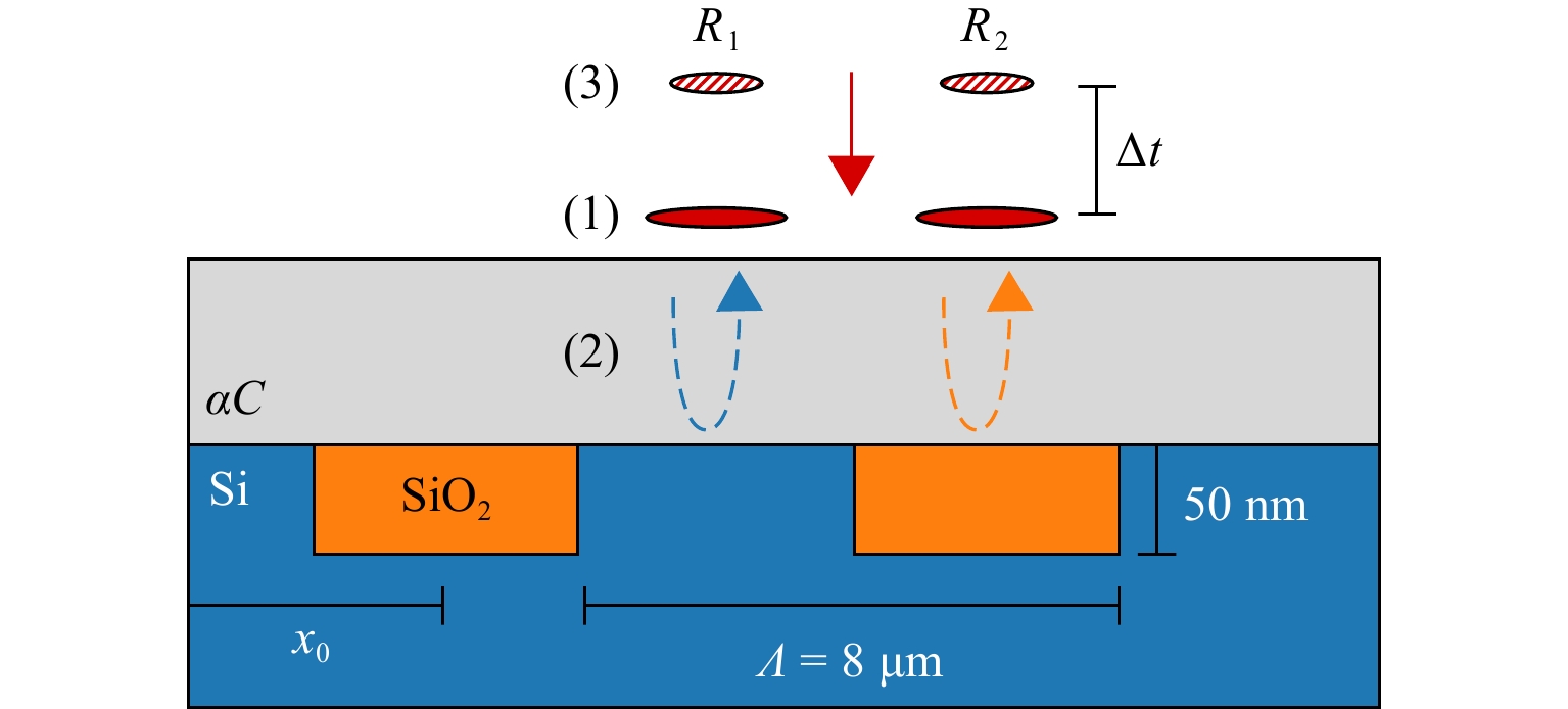
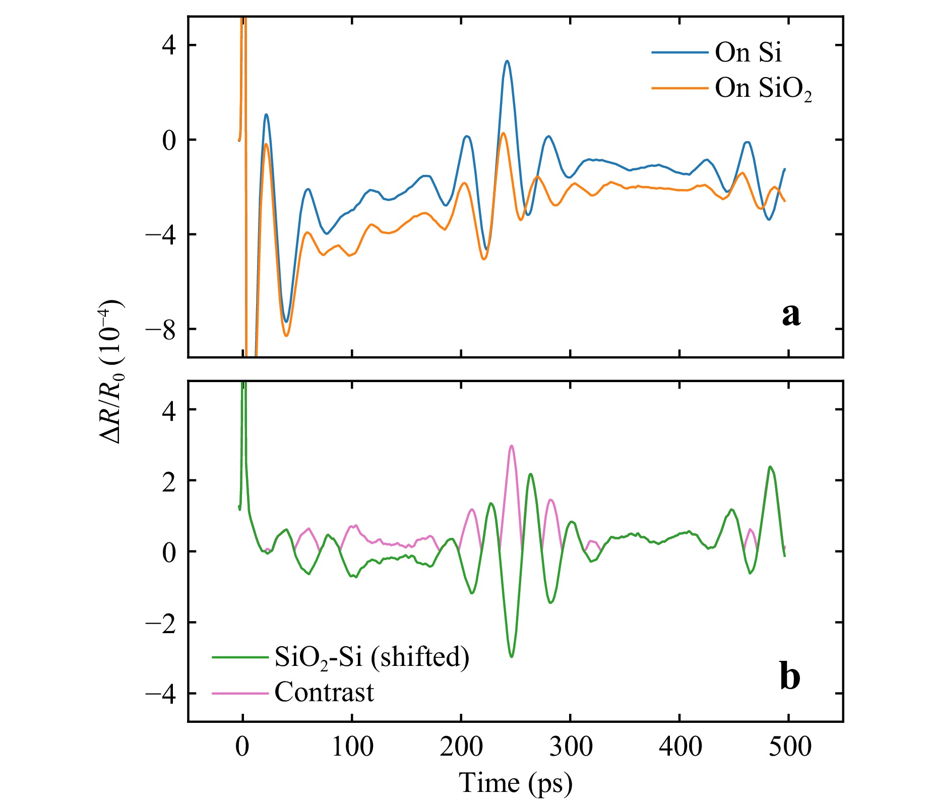
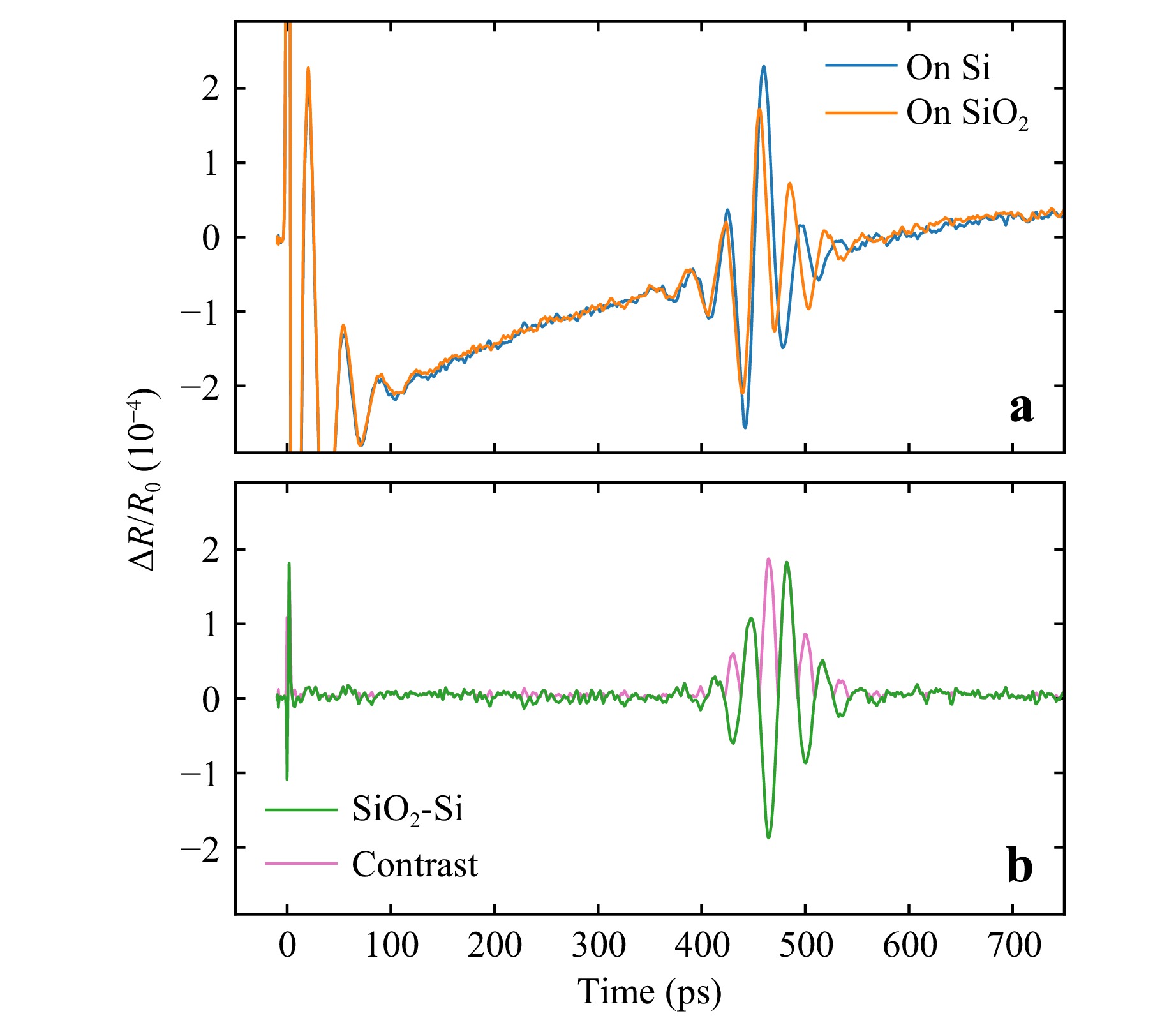
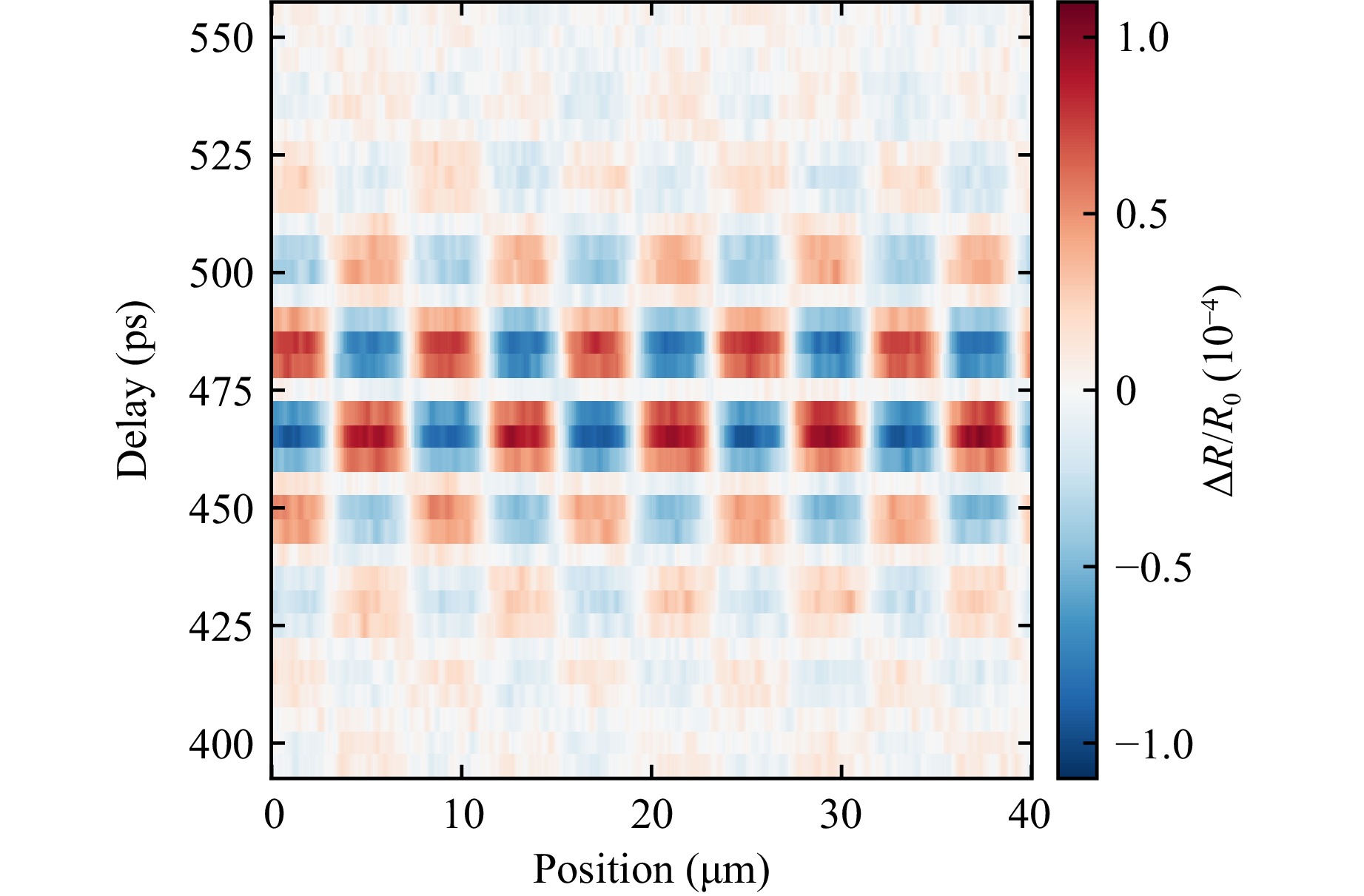
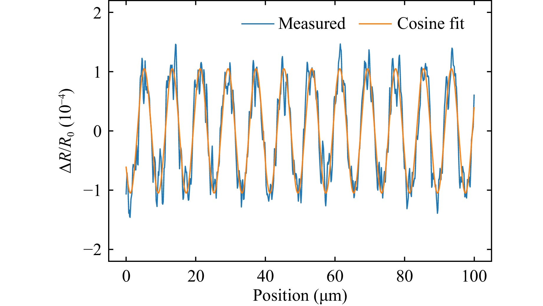
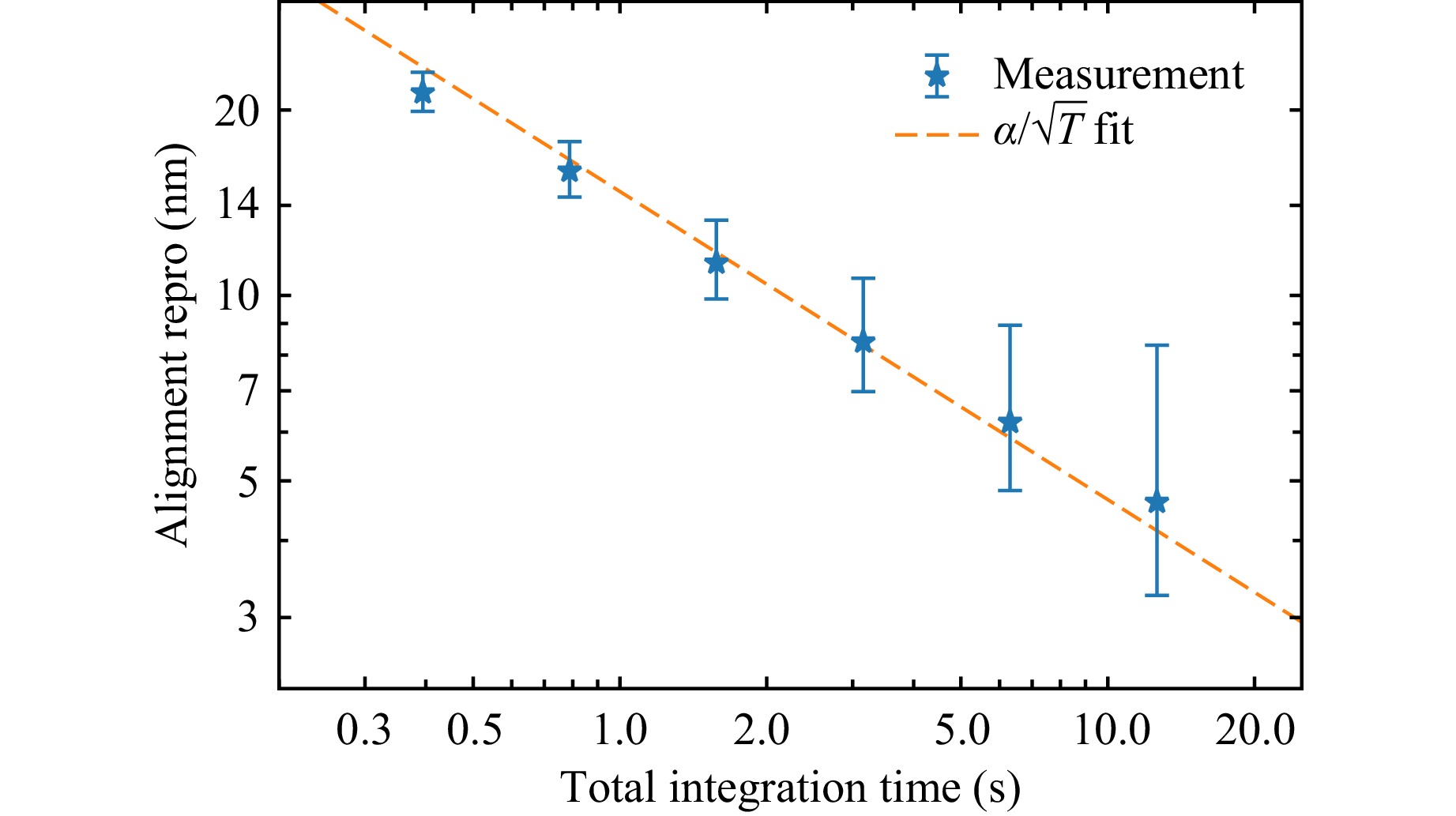
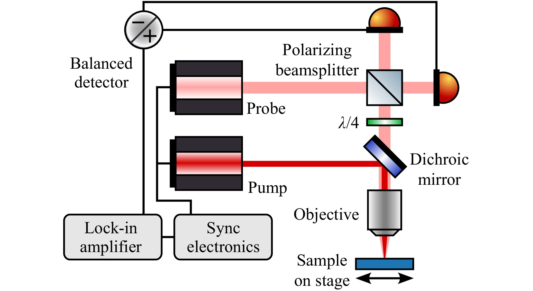
Manufacturing integrated circuits (ICs) using photolithography is the key technology enabling modern electronic devices. As advanced ICs are fabricated in multiple lithography steps, accurate metrology is crucial. For wafer alignment, optical methods are essential as they enable fast and non-invasive measurements. However, the use of optically opaque materials complicates optical metrology on markers in deeper layers. Here we present an optical metrology approach capable of nanometer-level alignment metrology through optically opaque layers. We use ultrashort laser pulses to generate high-frequency ultrasound at picosecond timescales, with which buried metrology markers can be probed. By detecting the ultrasound reflections with a second, time-delayed laser pulse, position information is obtained in an all-optical way. We demonstrate our approach on an alignment grating covered by a 1.3 μm thick layer of amorphous carbon, achieving 15 nm positioning reproducibility in 1 s measurement time, with significant potential for further scaling. This measurement concept will help advance semiconductor manufacturing, by enabling optical wafer metrology on future devices featuring layers of metals and other opaque materials.
Published. 2026, 7(3)
: 844-856
doi: 10.37188/lam.2026.075
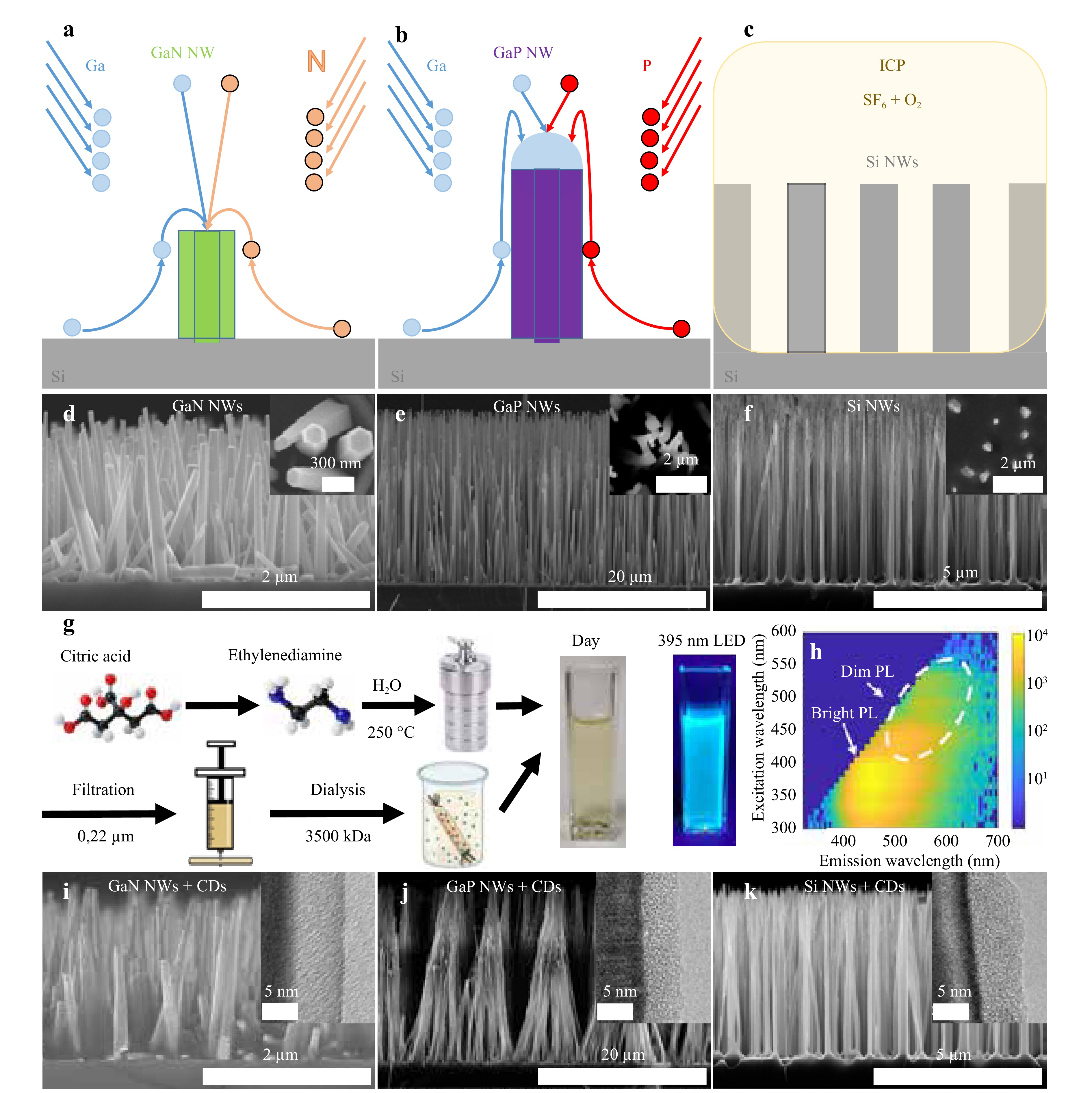
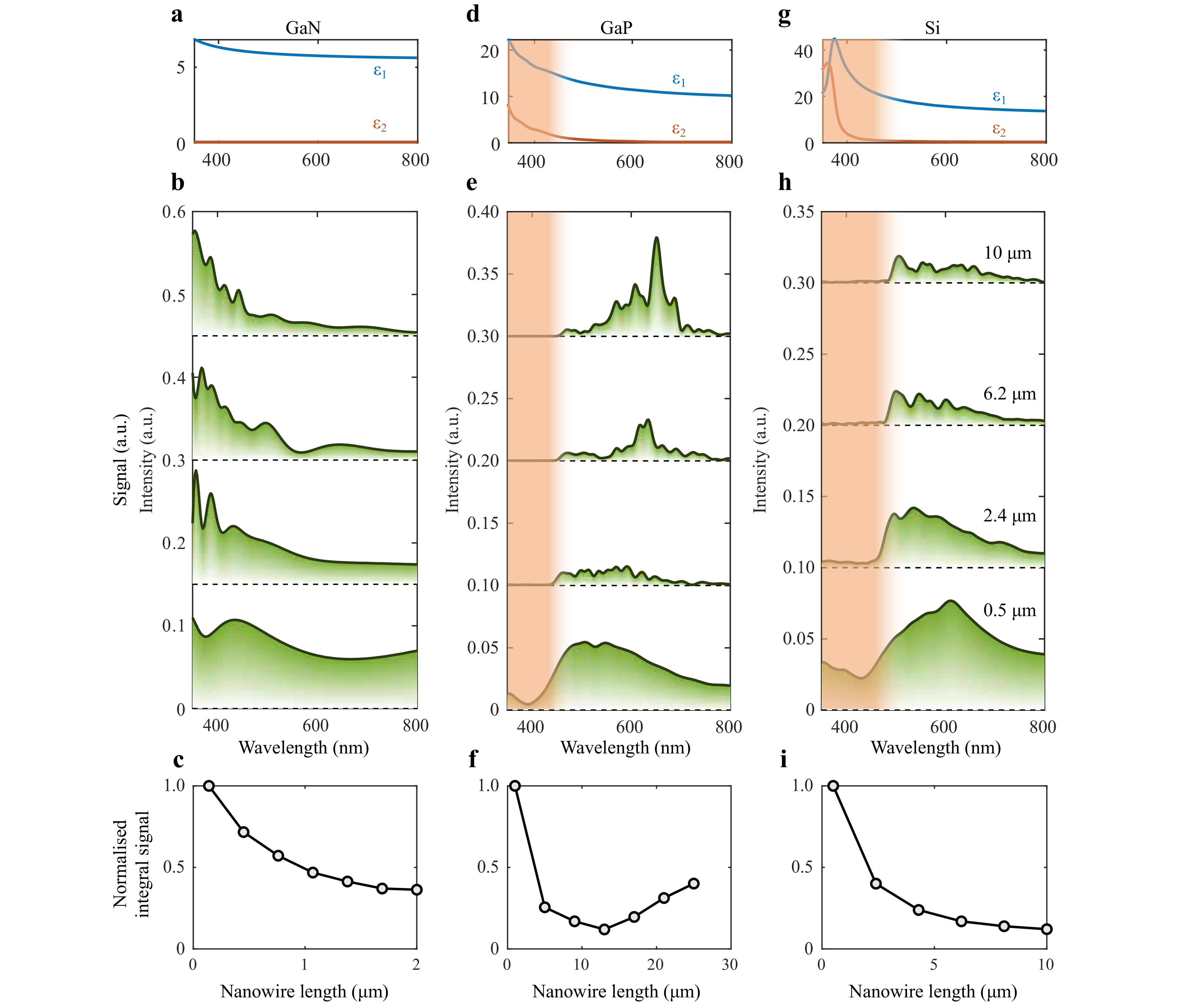
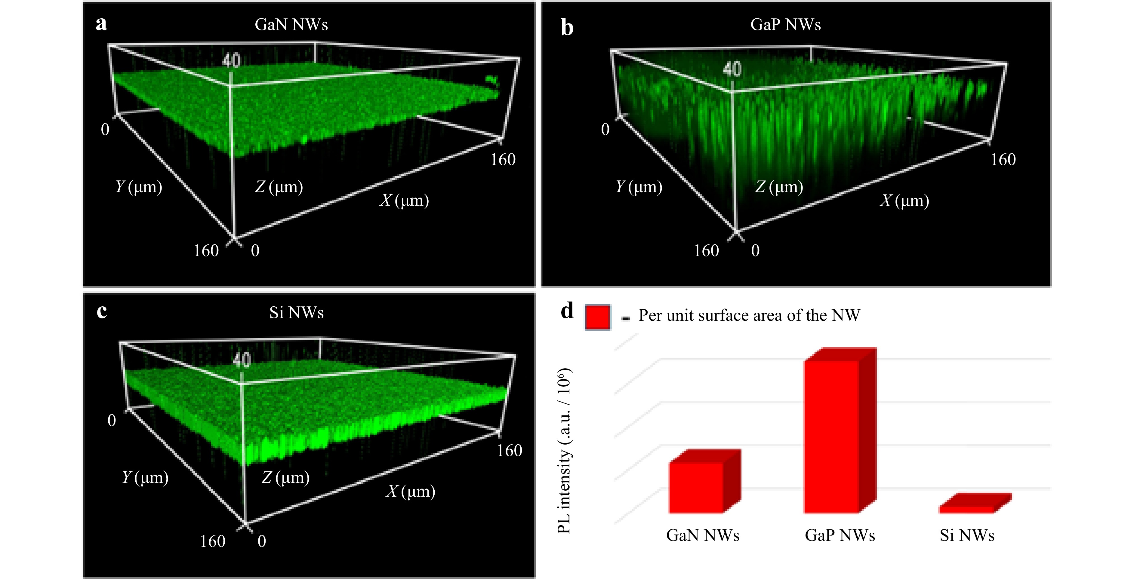
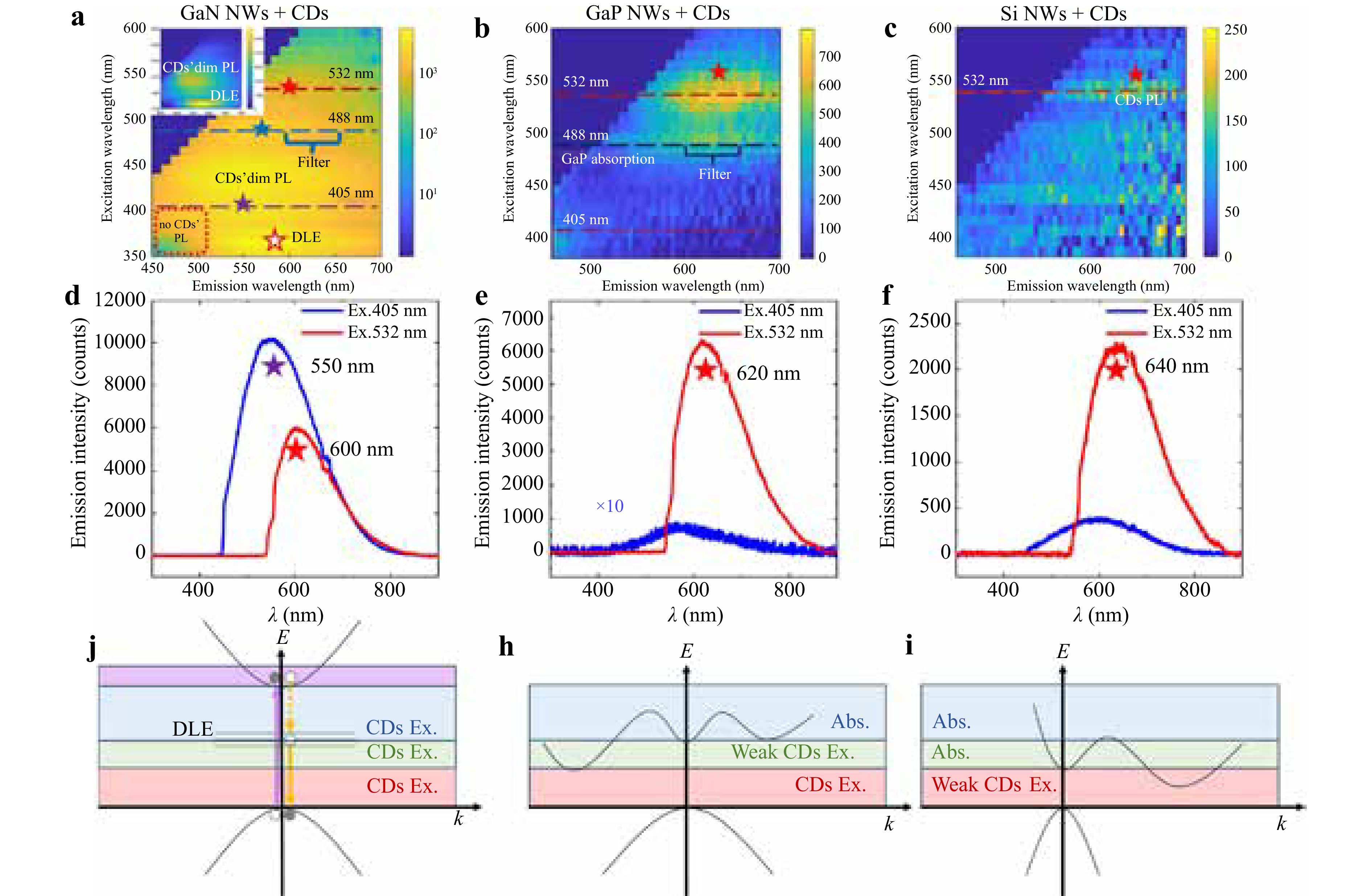
The integration of luminescent nanomaterials into scalable semiconductor platforms is vital for on-chip photonics. This study demonstrates an approach to fabricate fluorescent nanostructures by hybridising carbon dots (CDs) with semiconductor nanowires (NWs) grown on Si. We systematically investigated the photoluminescence of CDs on GaN, GaP, and Si NW hosts and demonstrated the key role of the absorption edge of the host as a practical spectral filter. Our results show that efficient CD excitation is governed by the transparency window of the NW, thereby allowing the precise tailoring of the emission spectrum through rational host selection. This effect has been consistently demonstrated in different materials. By coupling the tuneable chemistry of CDs with the tailored optoelectronics of semiconductor NWs, this study establishes a scalable host-guest architecture for engineering nanoscale light sources to promote applications in integrated photonic circuits and sensing.
Published. 2026, 7(3)
: 857-867
doi: 10.37188/lam.2026.022
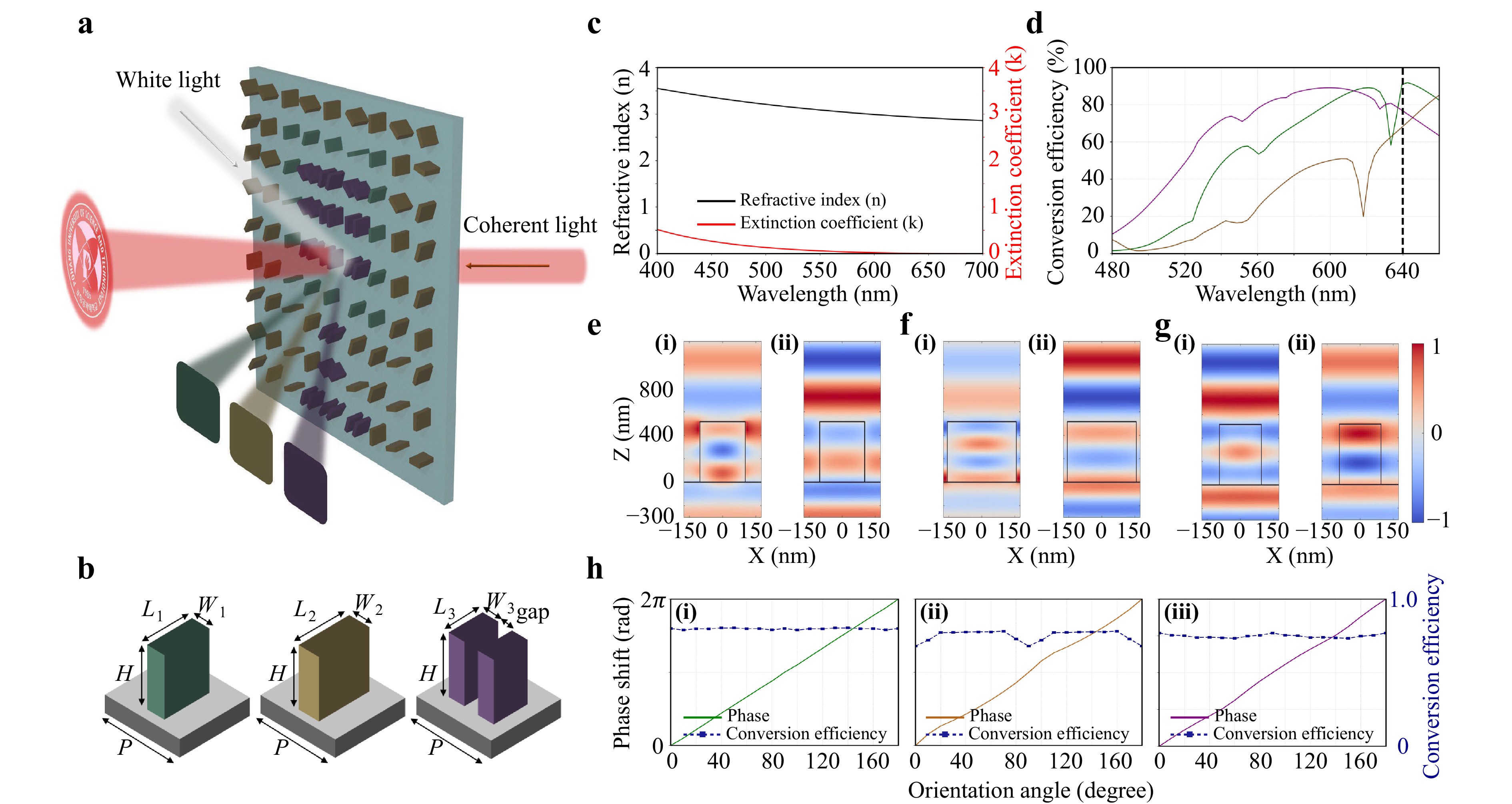
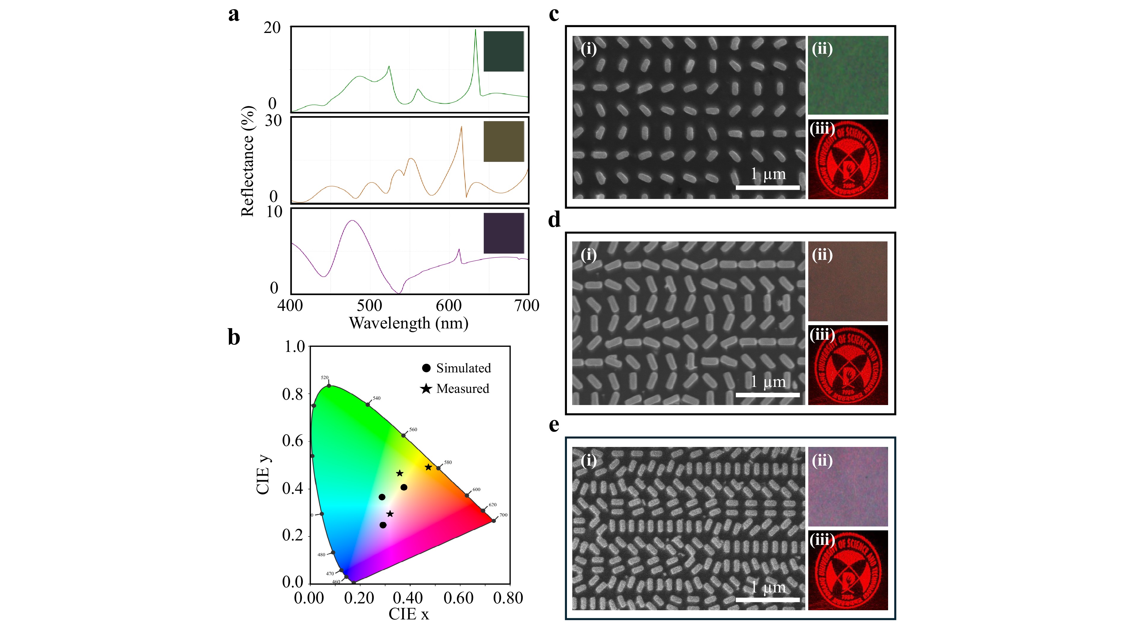
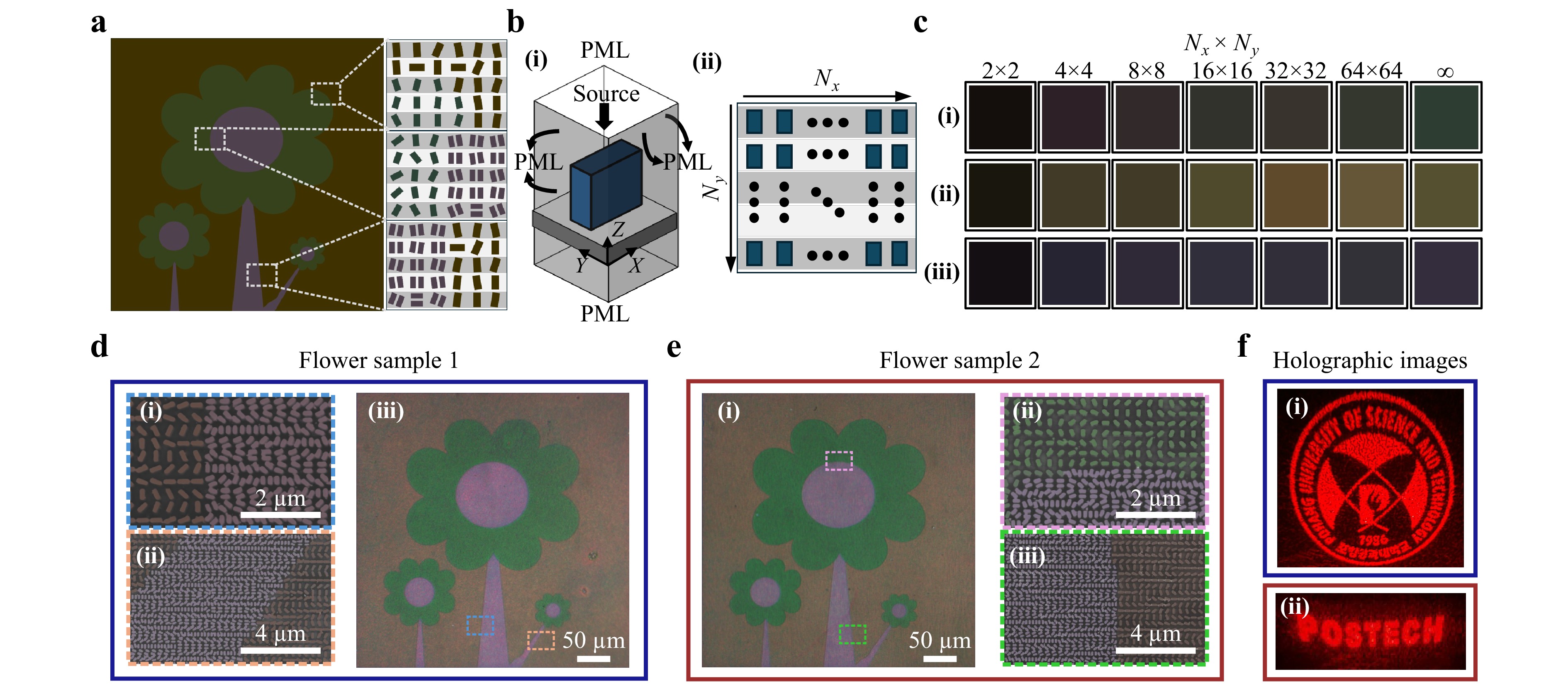
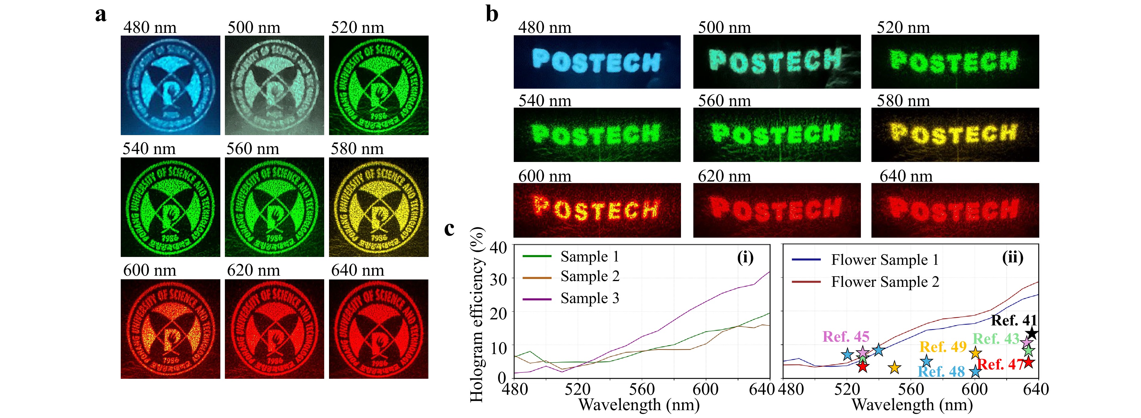
Metasurfaces, flat optical devices built from nanoscale structures, offer powerful and precise control over light. They have enabled applications such as structural color printing by manipulating spectral responses and holography through precise phase control. Integrating these functions into a single metasurface has gained interest for compact multifunctional platforms. However, most existing dual-mode designs suffer from low hologram efficiency, limiting their practical applications in multifunctional optical systems. Here, we present dual-functional metasurfaces that simultaneously enable three-color structural printing under white light illumination and high-efficiency holography under coherent light. Our design employs three distinct meta-atoms, composed of single and double nanorods, to achieve independent spectral and phase modulations. The metasurfaces produce three distinct reflective colors of green, brown, and magenta and achieve numerical conversion efficiency up to 90% at the 640 nm wavelength. The fabricated devices successfully display desired structural colors under white light and reconstruct holographic images with high efficiency under coherent illumination. The devices also demonstrate broadband performance for holography across the visible spectrum. These results confirm the effectiveness of our design in achieving independent and efficient control of color and holography within a single metasurface. This multifunctional capability offers strong potential for applications in anti-counterfeiting and compact optical data storage.
Published. 2026, 7(3)
: 868-875
doi: 10.37188/lam.2026.086
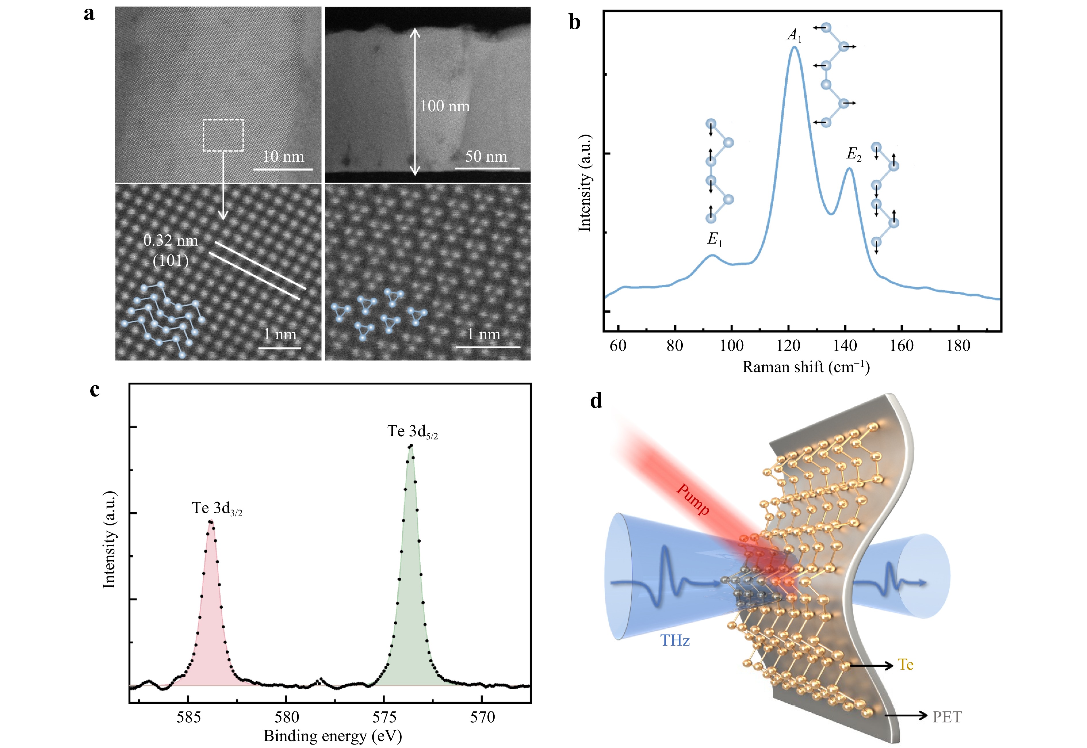
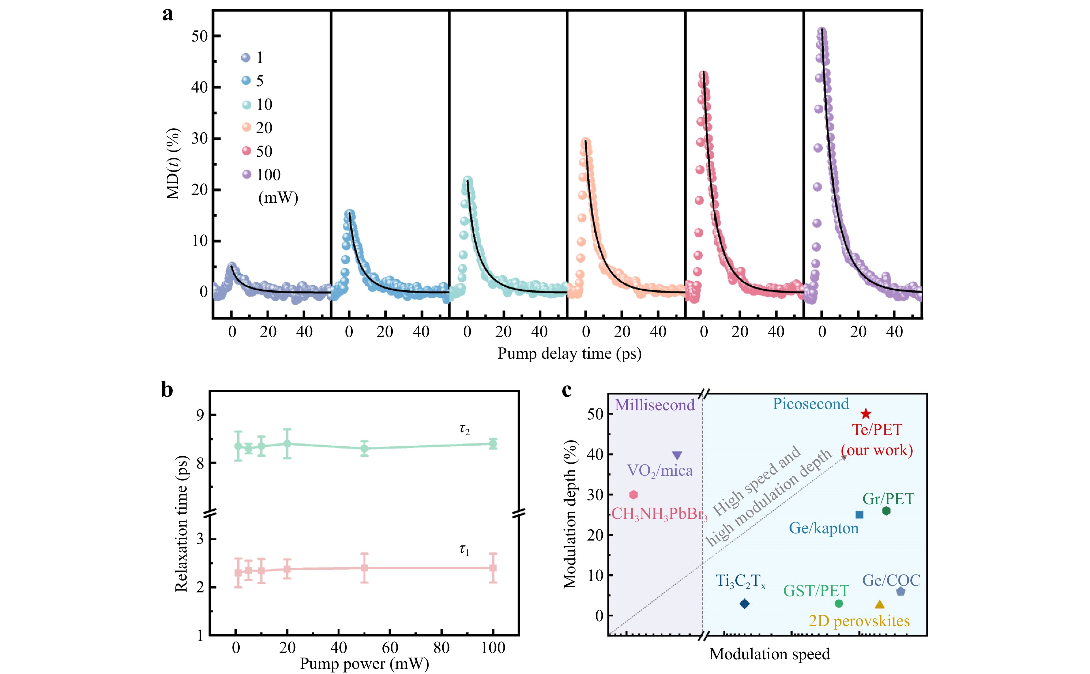
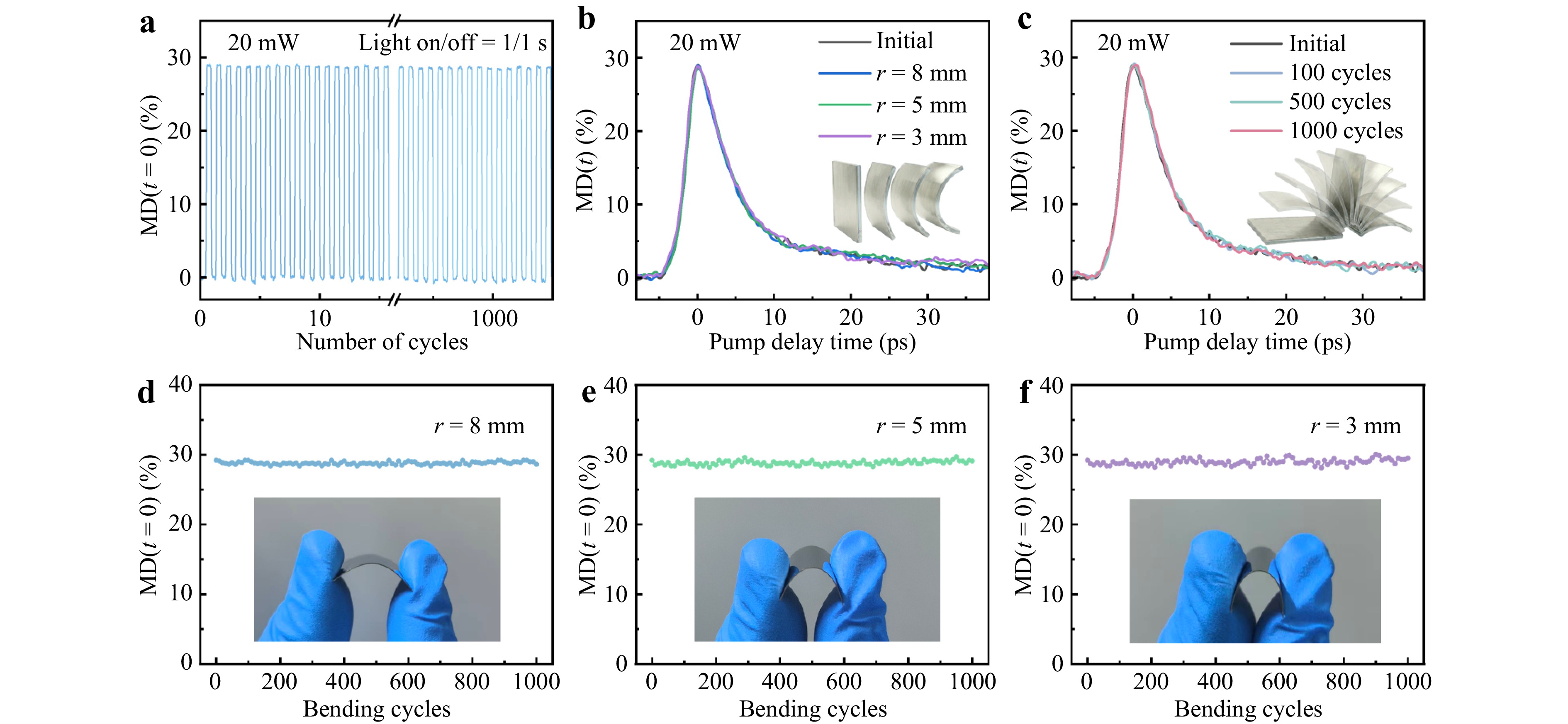
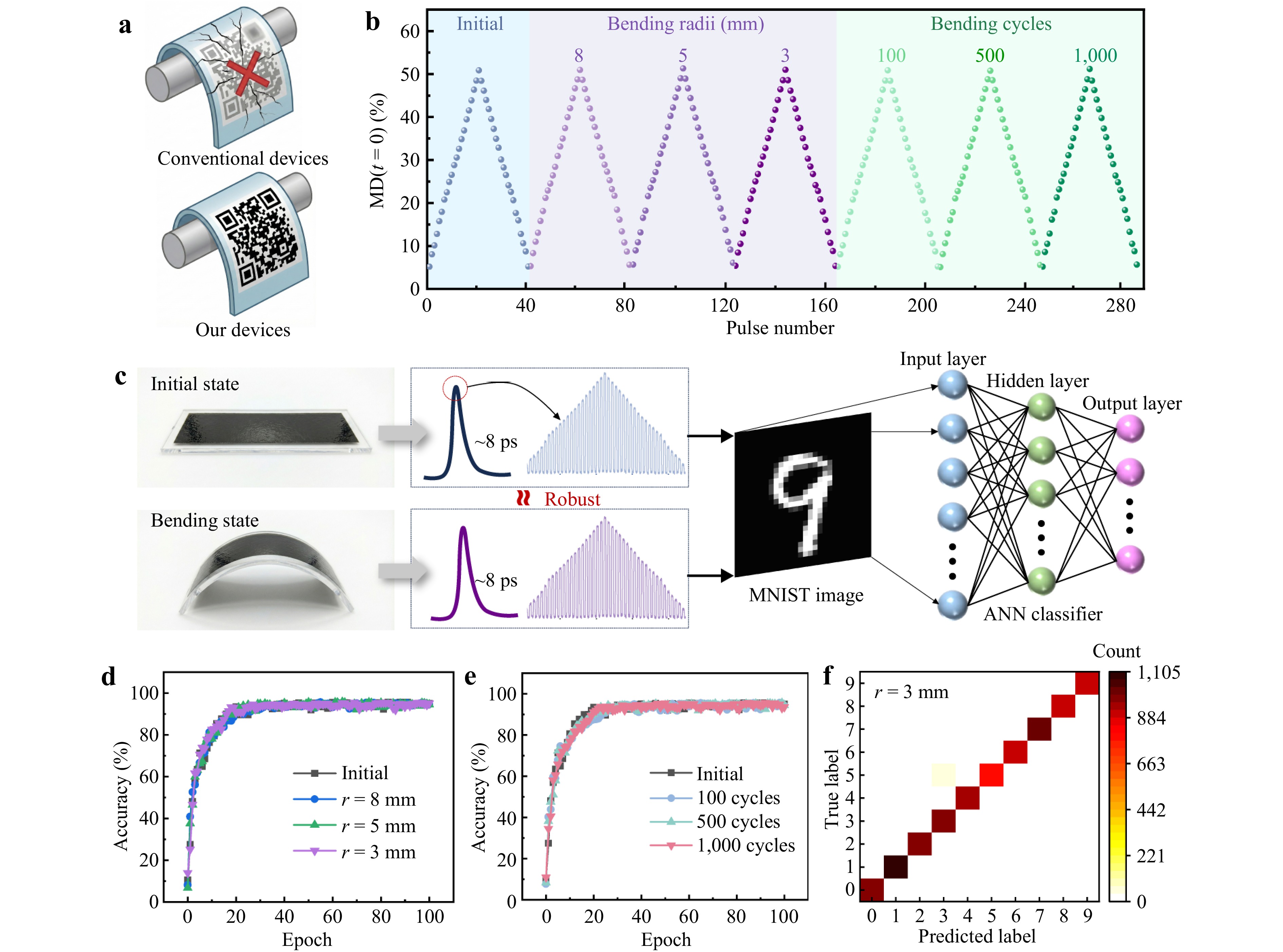
Flexible terahertz (THz) devices are fundamental components of wearable photonics and intelligent communication systems. However, conventional THz devices are affected by information loss or signal interruption due to mechanical deformation, which degrade their information fidelity. Here, we introduce tellurium (Te) nanofilms grown on polyethylene terephthalate (PET) substrates as a new class of mechanically robust THz modulators that can successfully improve device performances to optimal levels among existing flexible broadband modulators. The ultrafast transient THz photoresponses of two-dimensional Te films remained unchanged even after 1000 bending cycles or at a small bending radius of 3 mm, exhibiting high tolerance to bending deformation. Furthermore, the variations in the pattern recognition accuracy remained within 2% under different bending conditions, indicating its adaptability to various deformation conditions. This prototype lays the foundation for developing intelligent perception elements that operate stably under complex mechanical deformations.
Published. 2026, 7(3)
: 876-891
doi: 10.37188/lam.2026.088
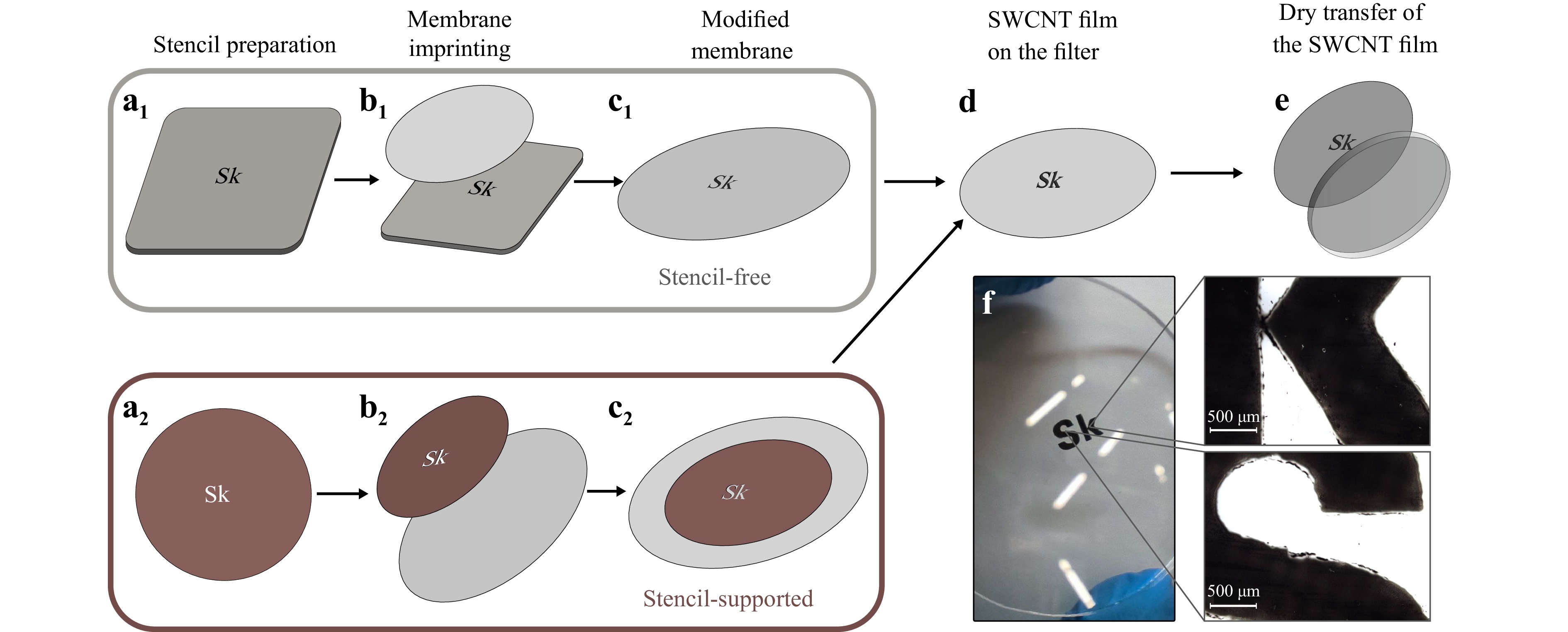
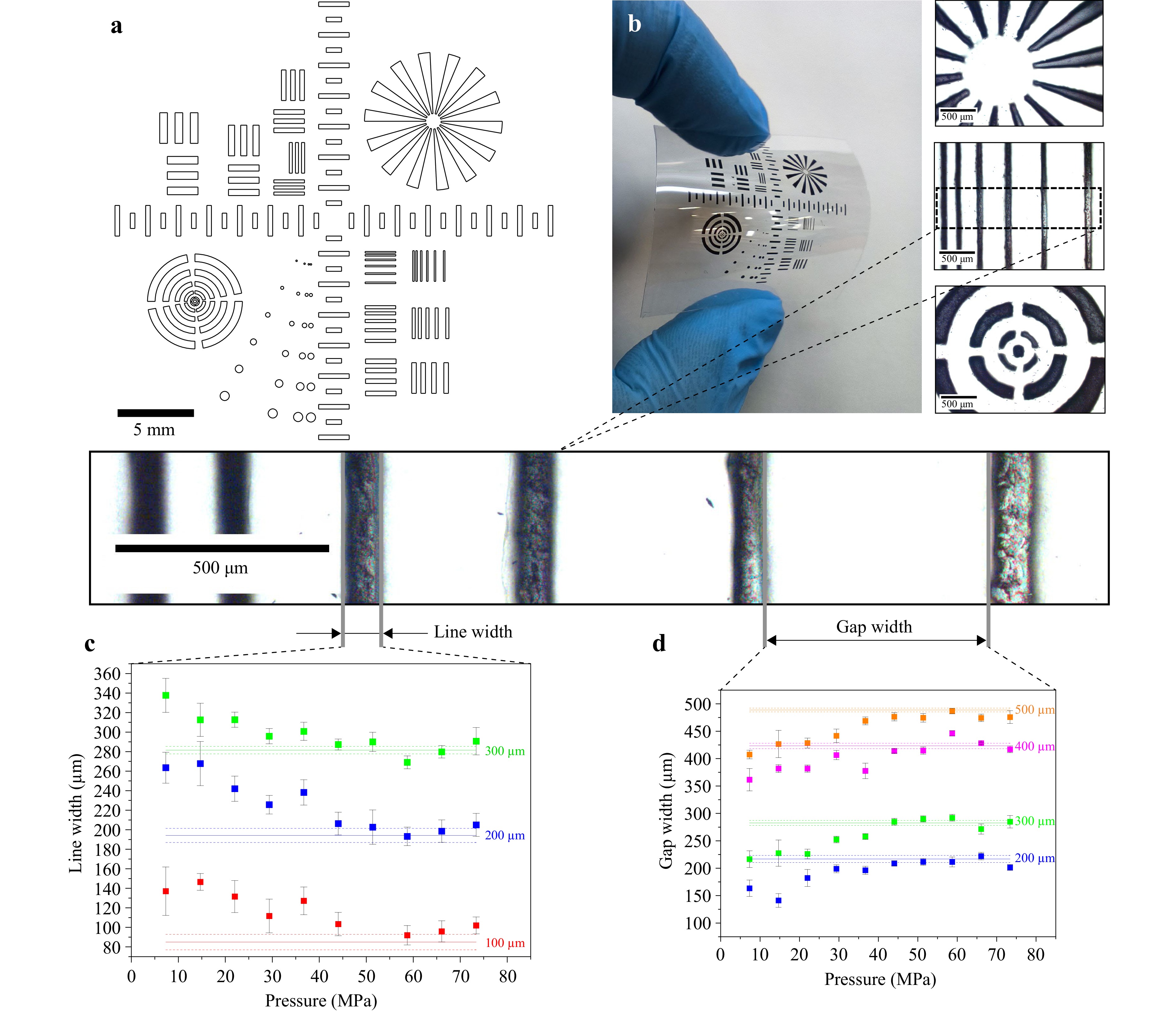
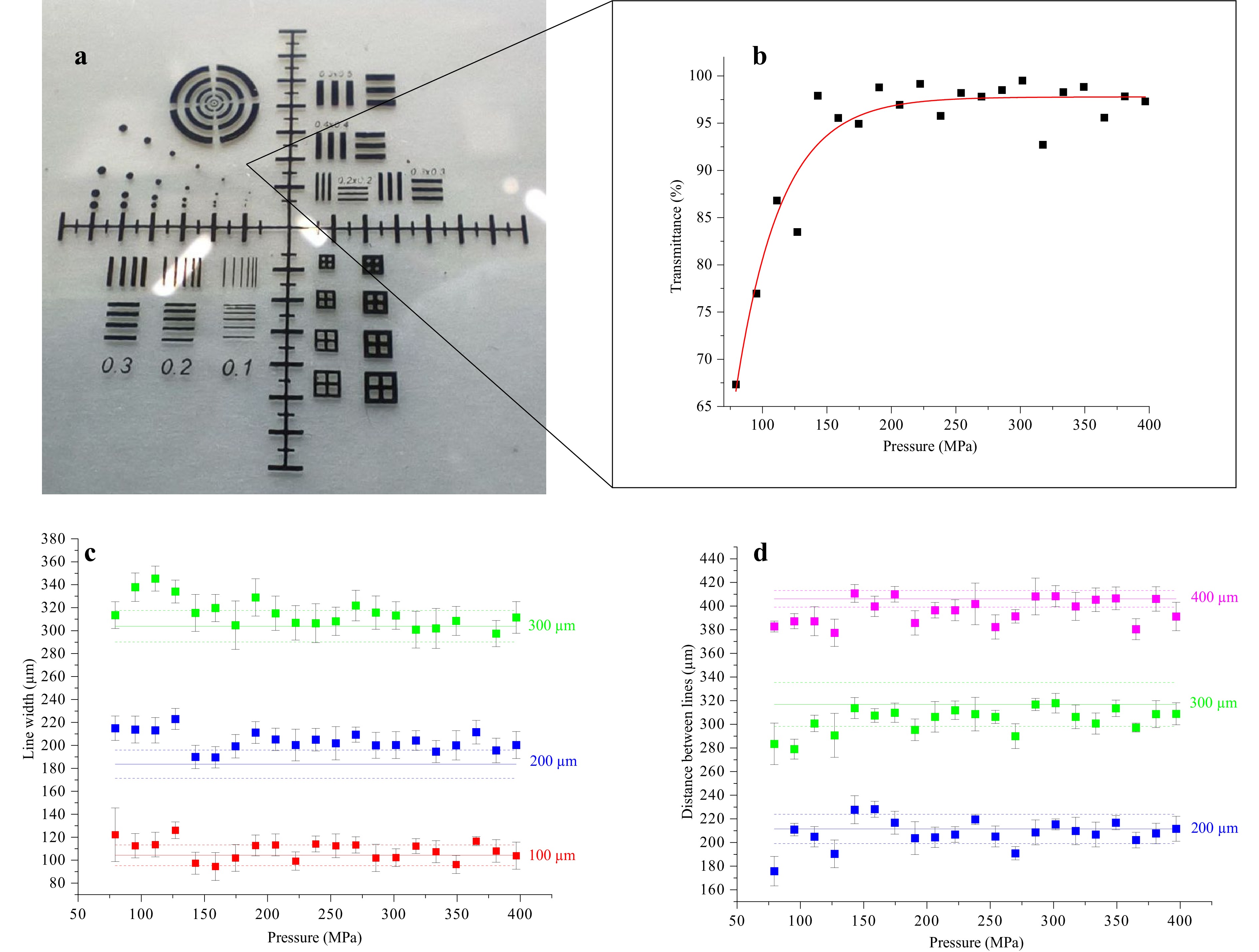
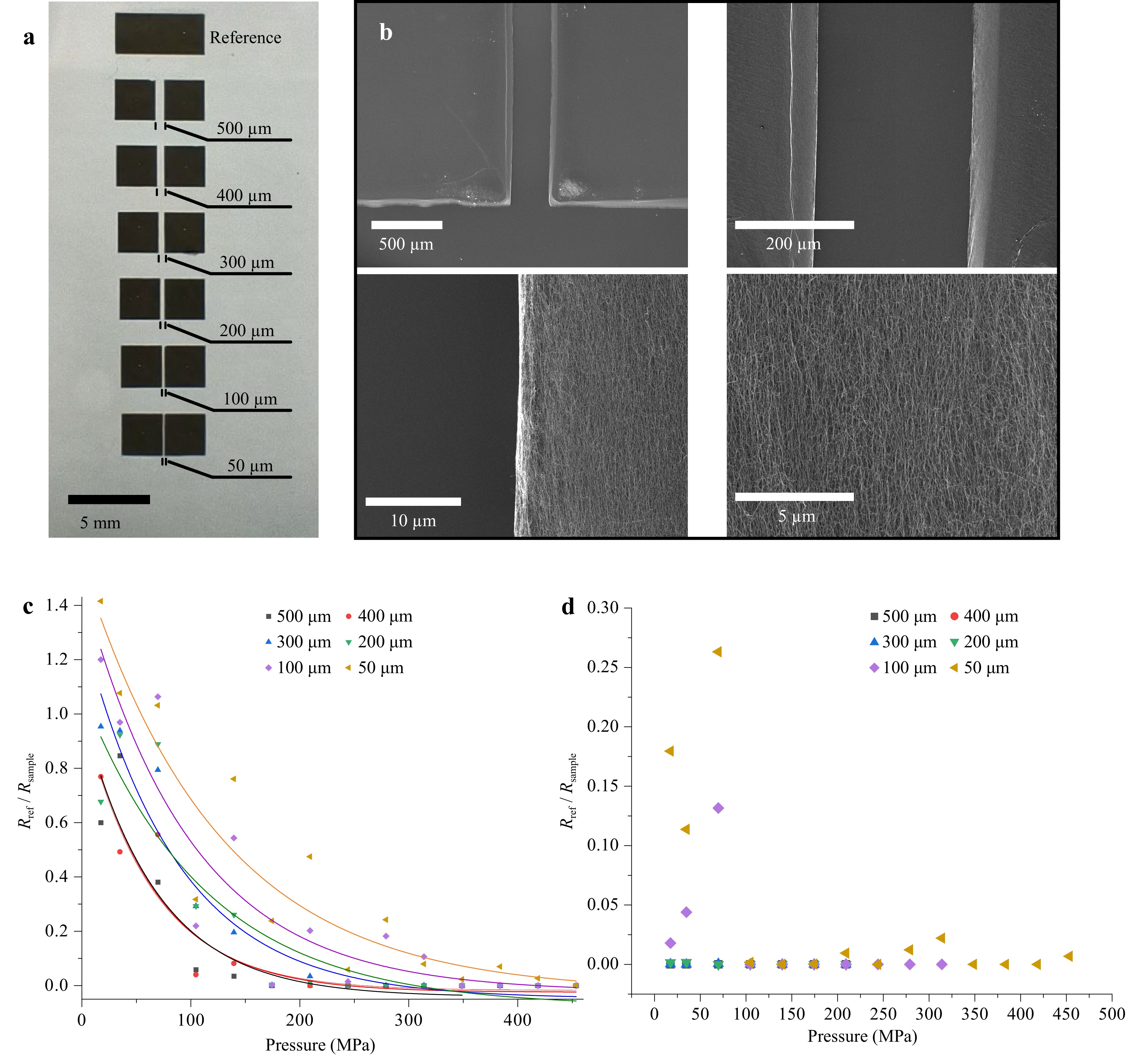
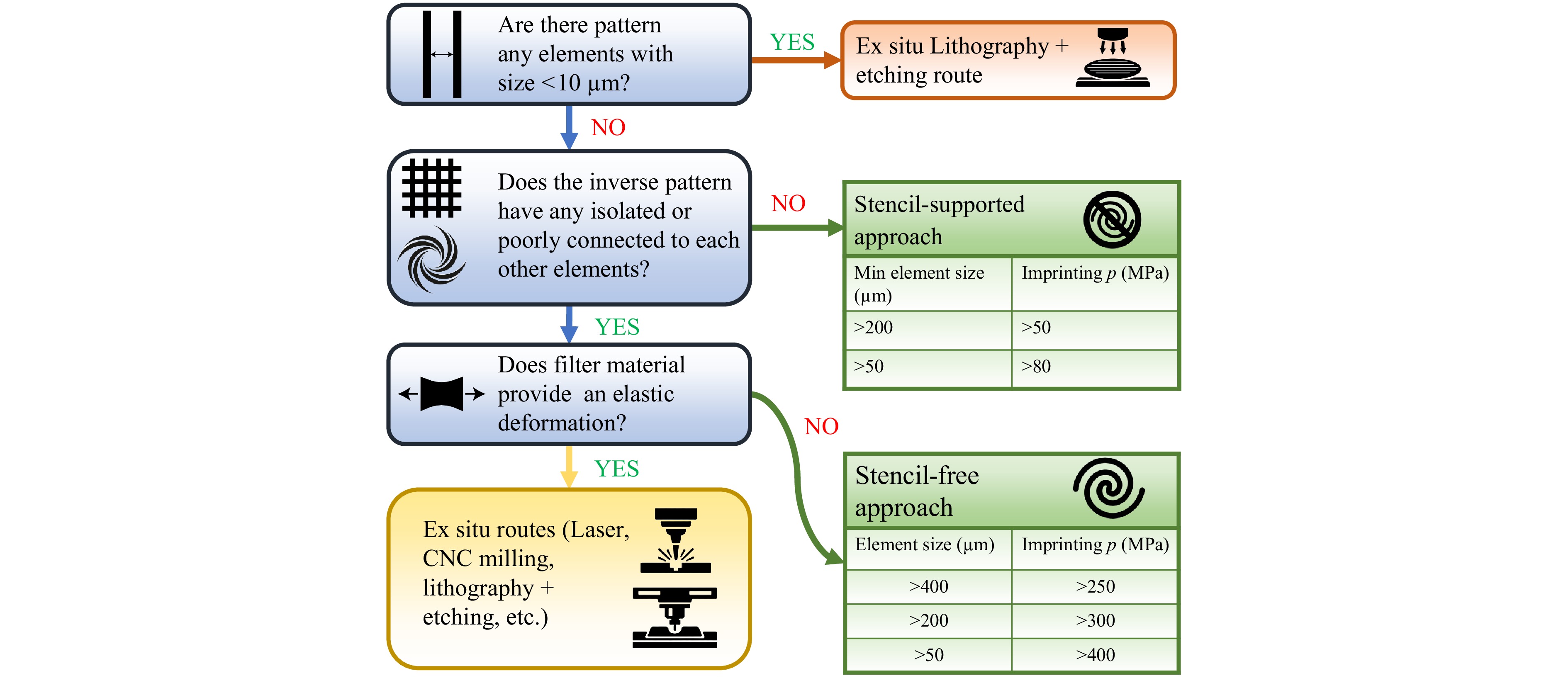
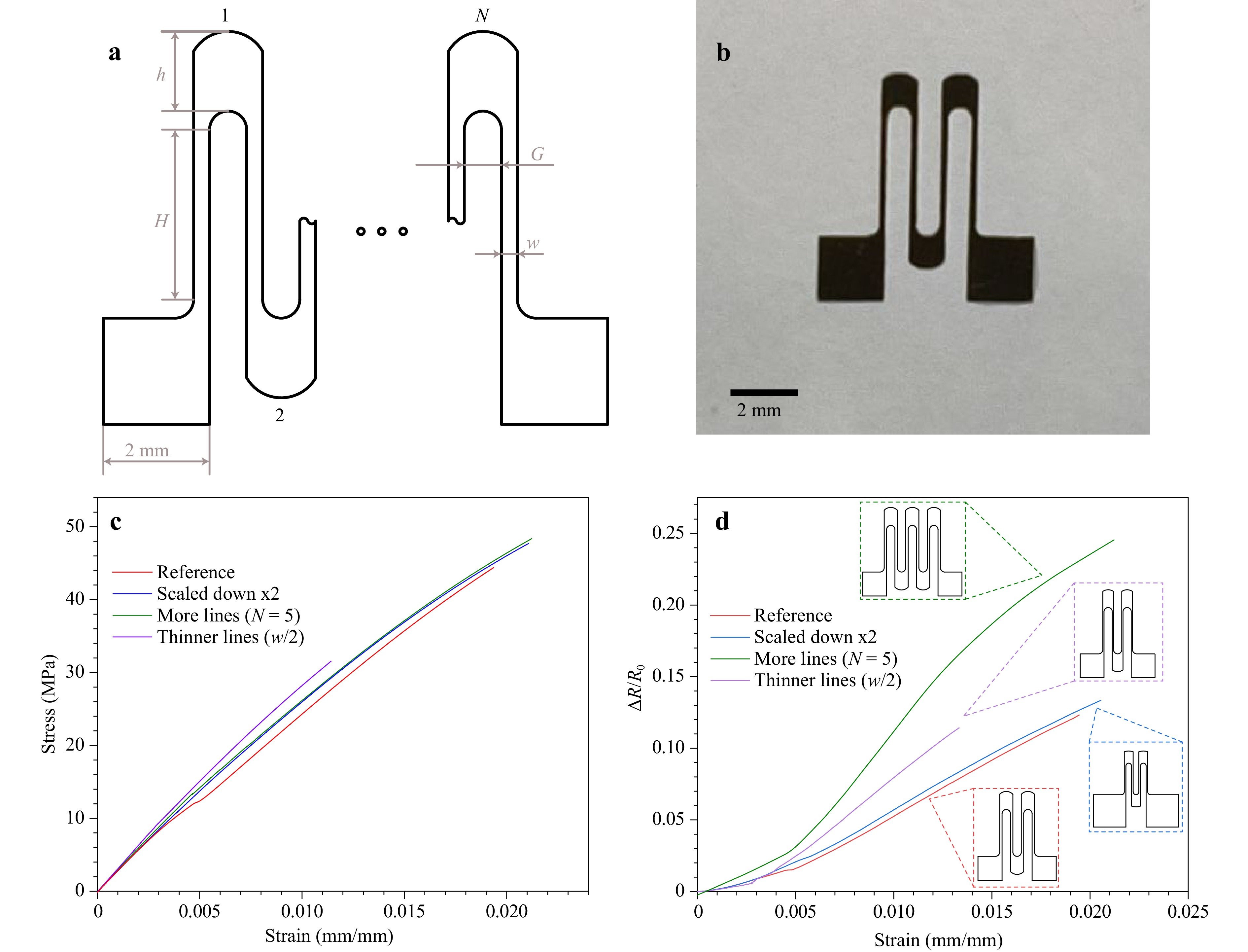
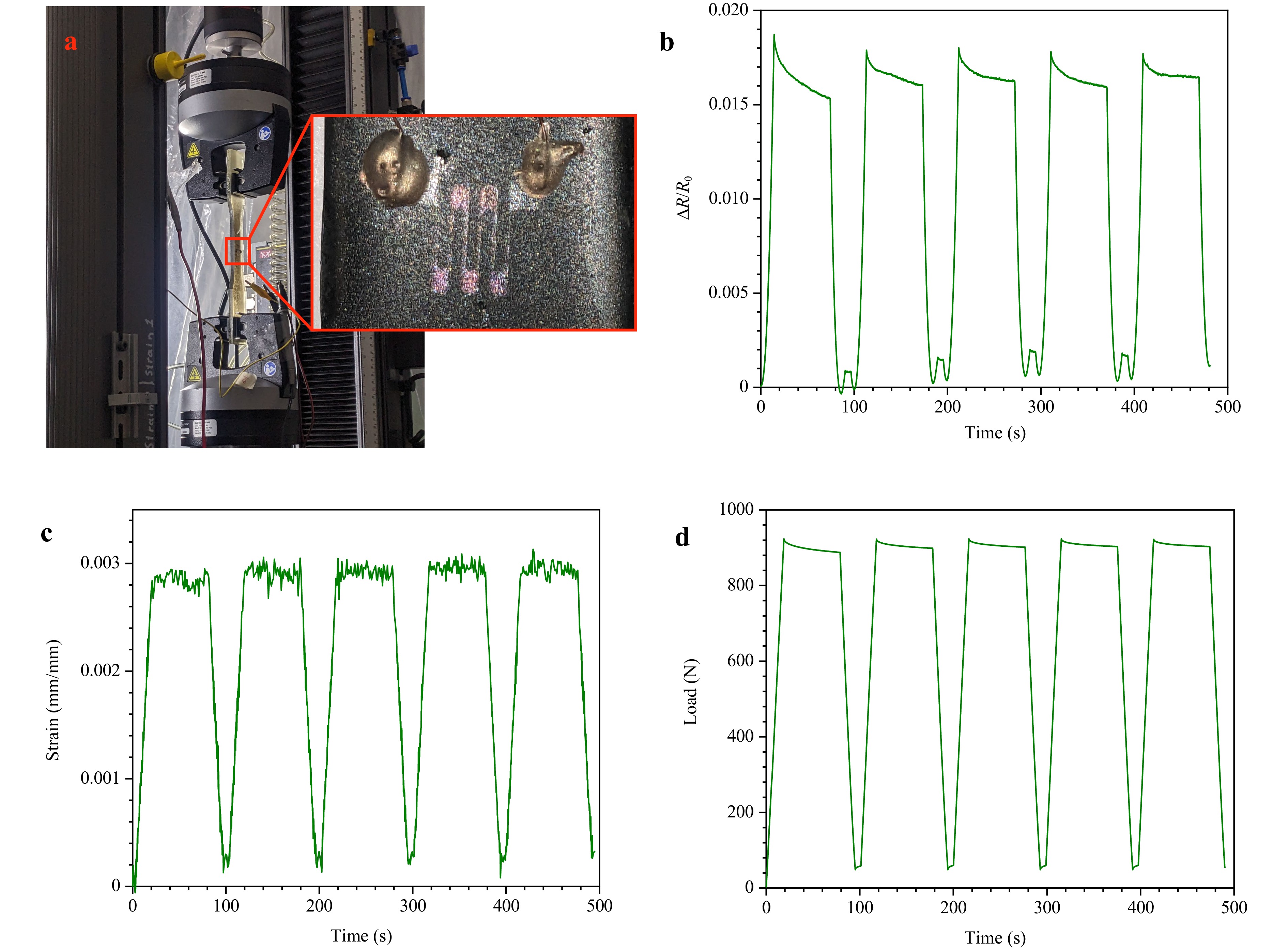
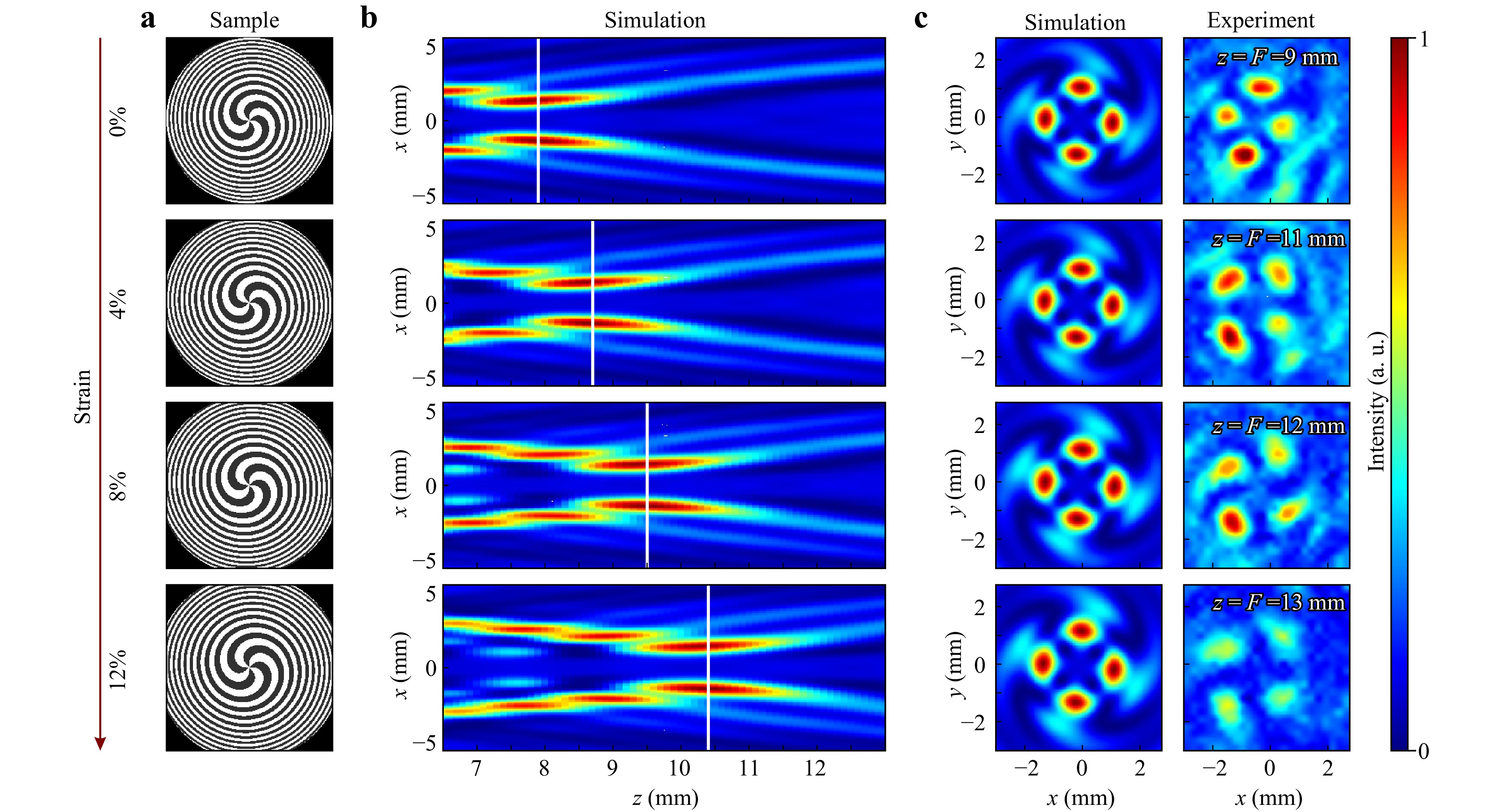
Being one of the most prominent topics, the development of the optically active devices based on lenses and metasurfaces lacks a robust material basis suitable for the terahertz (THz) range. Among candidates such as graphene and dichalcogenides, single-walled carbon nanotube (SWCNT) films offer high modulation depth, durability, and scalability, but precise spatial patterning remains challenging. We present a waste-free, one-step, dry patterning approach that combines aerosol chemical vapor deposition (CVD) with spatially controlled aerosol flow clogging via stencil imprinting. Two approaches are demonstrated. In the stencil-free variant, stencil removal after imprinting yields reproducible features >200 μm and near-complete nanotube suppression in clogged regions at pressures above 200 MPa. In the stencil-supported variant, retaining the stencil enhances flow blocking, achieving complete nanotube exclusion at lower pressures (~100 MPa) and enabling finer features approaching laser resolution. The method is validated through two applications: strain sensors with at least threefold improved response than reported values, and a mechanically tunable THz spiral zone plate with focal shifts up to 44% under 12% strain. This imprinting method offers a scalable route to precisely patterned SWCNT films and opens new opportunities for integrating CNT-based patterns into THz optics and electronic devices.
Published. 2026, 7(3)
: 892-902
doi: 10.37188/lam.2026.089
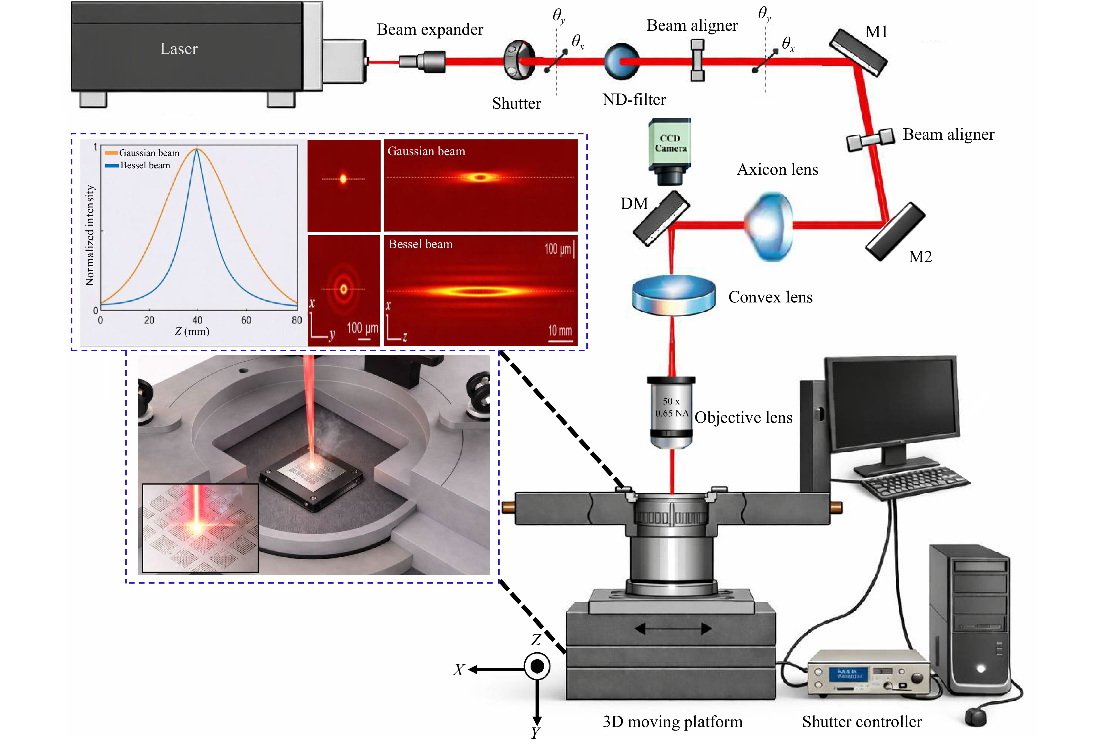
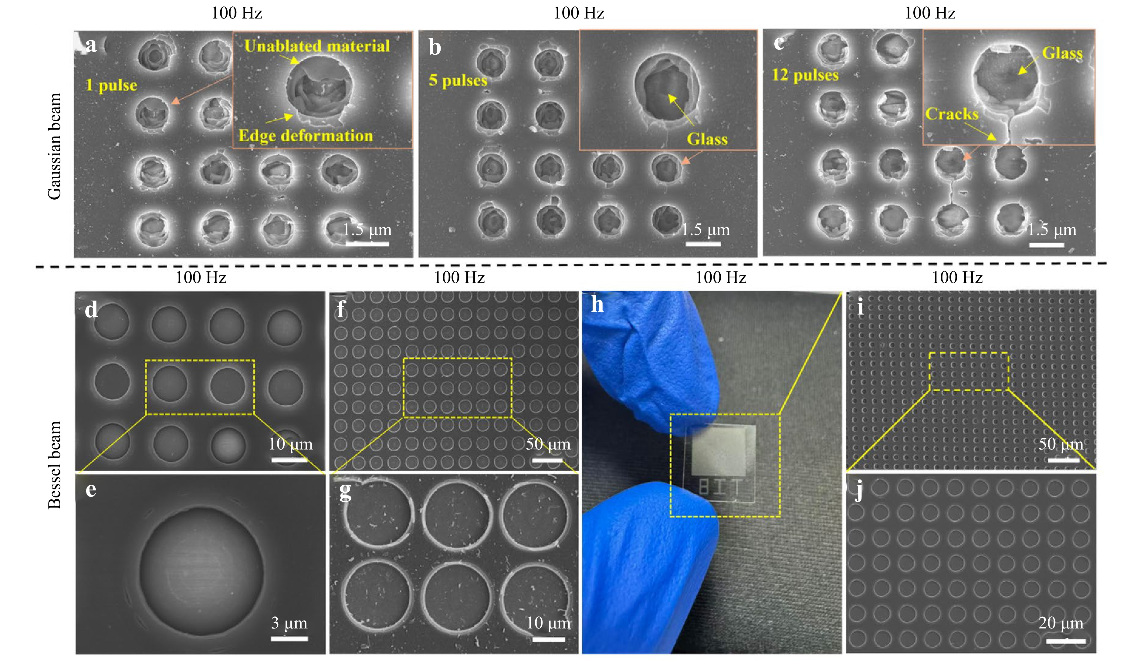
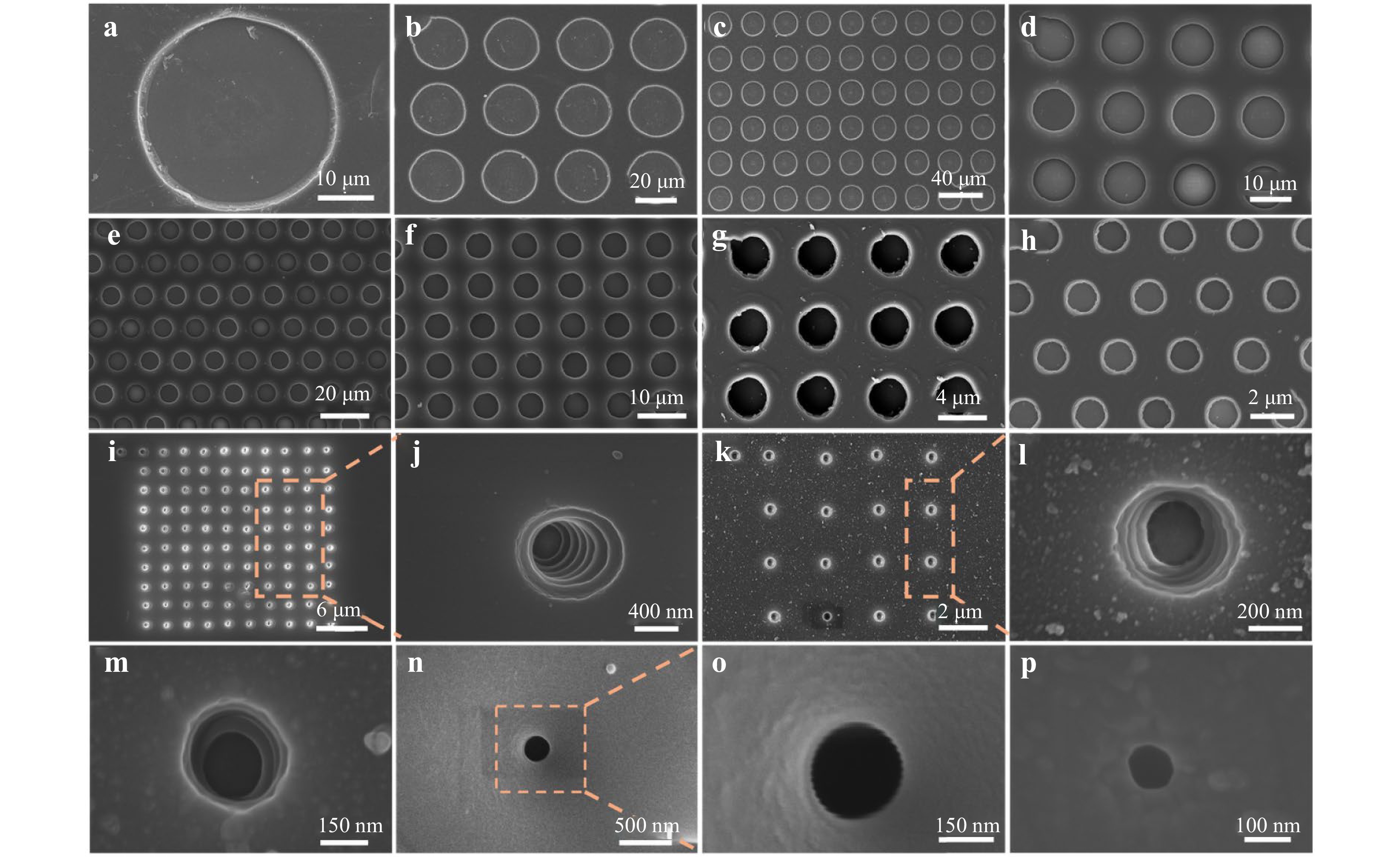
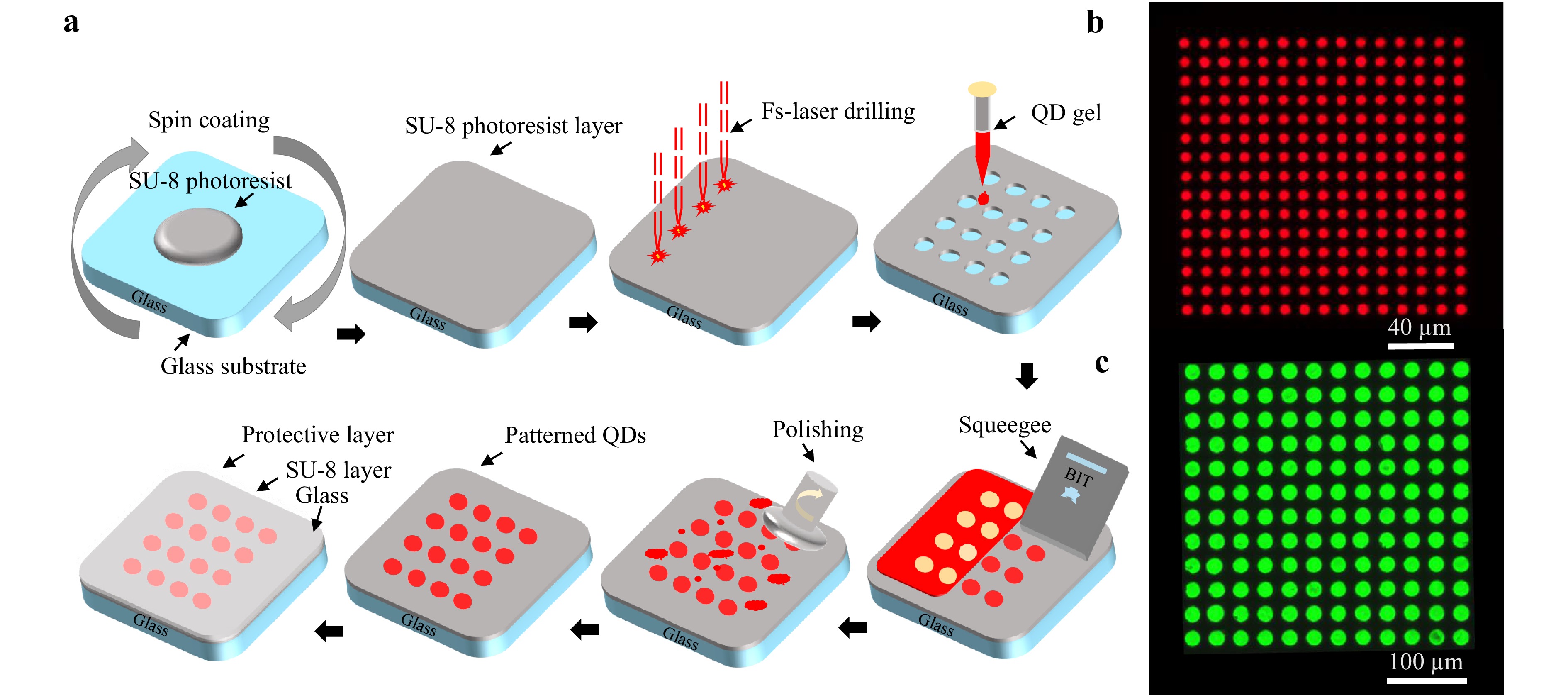
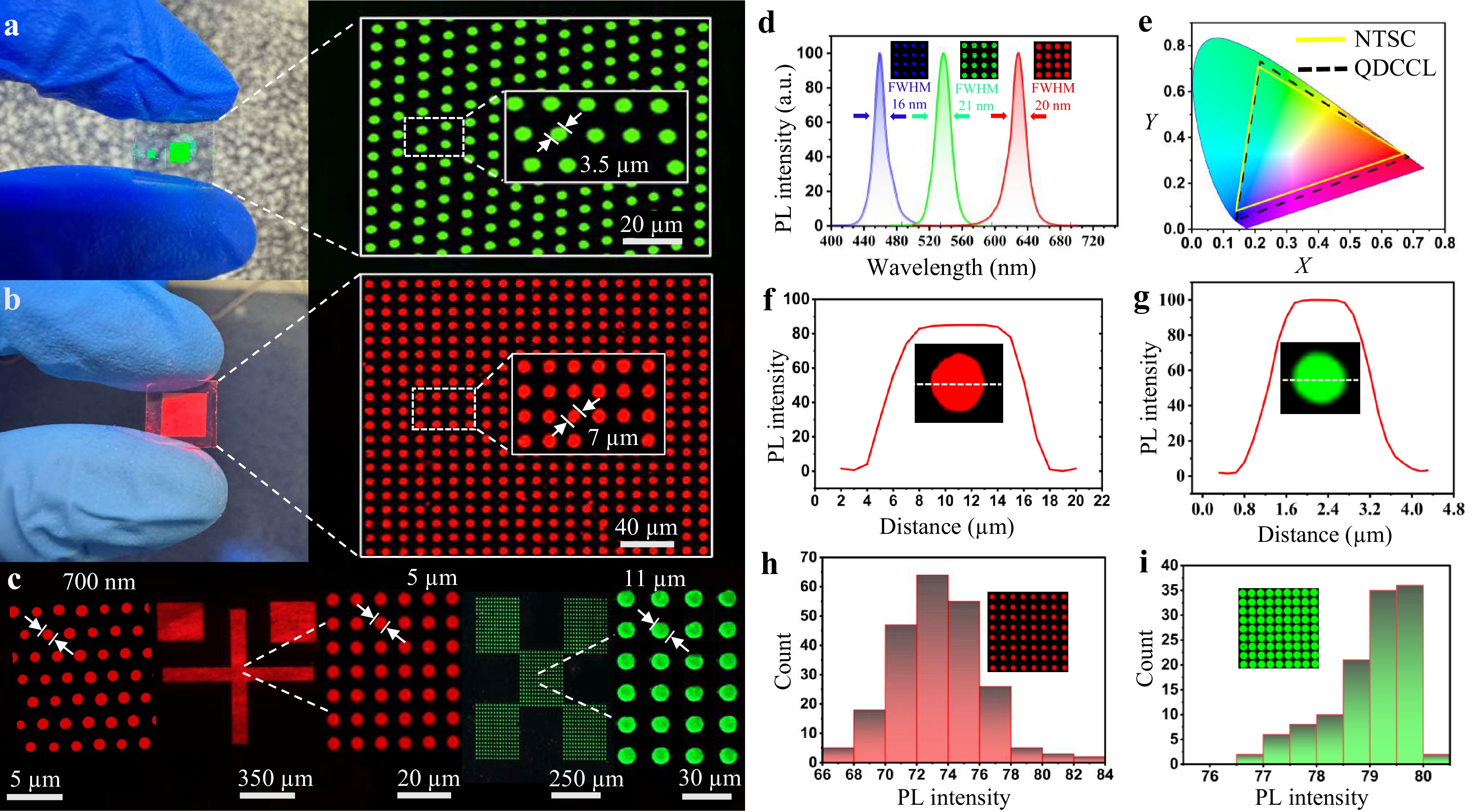
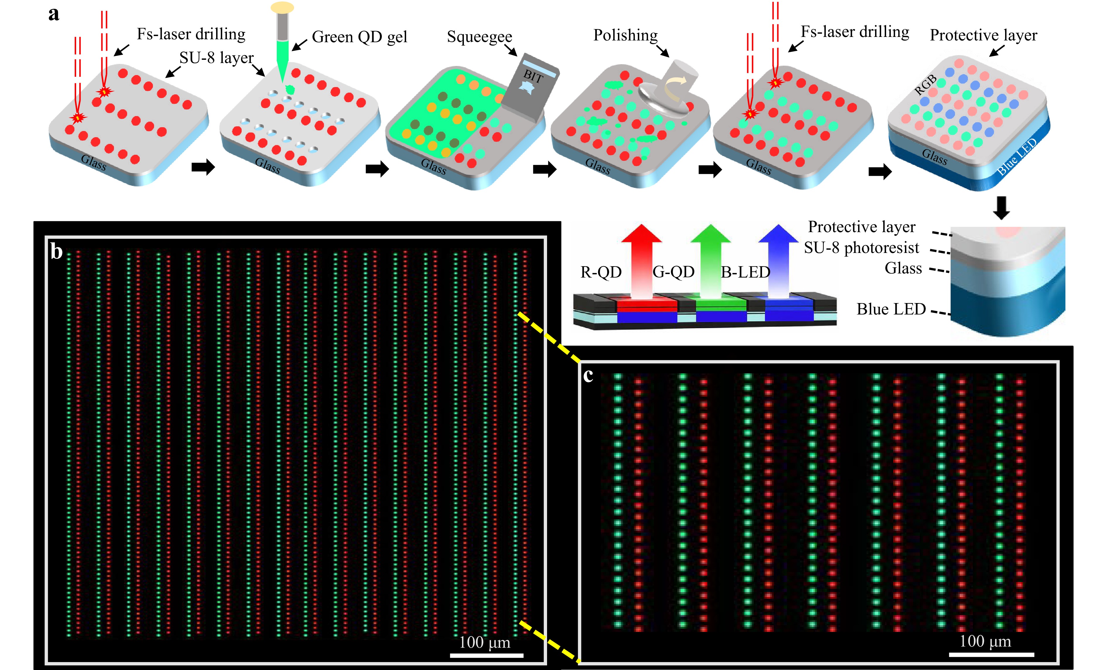
High-resolution pixelated patterning of quantum dot colour-conversion (QDCC) layers is of significant importance for advancing display technologies. However, a significant challenge lies in the fabrication of high-resolution pixel templates with submicron precision and geometric uniformity. In this study, a high-precision and scalable femtosecond (fs) laser drilling method is used to fabricate microhole arrays in SU-8 polymers. The results show that, compared with Gaussian beams, Bessel-beam irradiation enables the formation of taper-free microholes with smooth sidewalls and diameters as small as 100 nm, while preventing damage to the underlying glass substrate. The fabricated microholes are used as a micropore mould to fabricate monochrome and dual-colour QDCC layers by precisely filling them with CdSe QDs. These layers exhibit narrow-band fluorescence with full widths at half maximum (FWHMs) of 21 nm (green) and 20 nm (red), high colour purity, and a wide colour gamut reaching 111% of the National Television System Committee (NTSC) standard. Pixel-level photoluminescence (PL) mapping confirms homogeneous emission, with 93% of both red- and green-pixel intensities falling within narrow ranges and luminous uniformities of 90% and 97%, respectively. This maskless and solvent-free process offers a promising platform for high-resolution QDCC layers in augmented reality/virtual reality (AR/VR) systems and next-generation micro-light-emitting diode (micro-LED) displays.
Published. 2026, 7(3)
: 903-912
doi: 10.37188/lam.2026.082
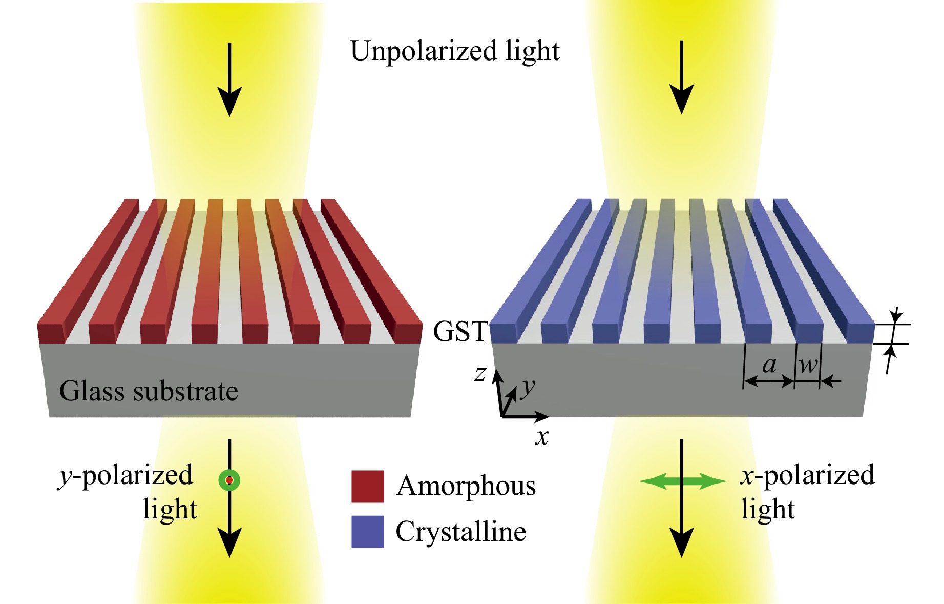
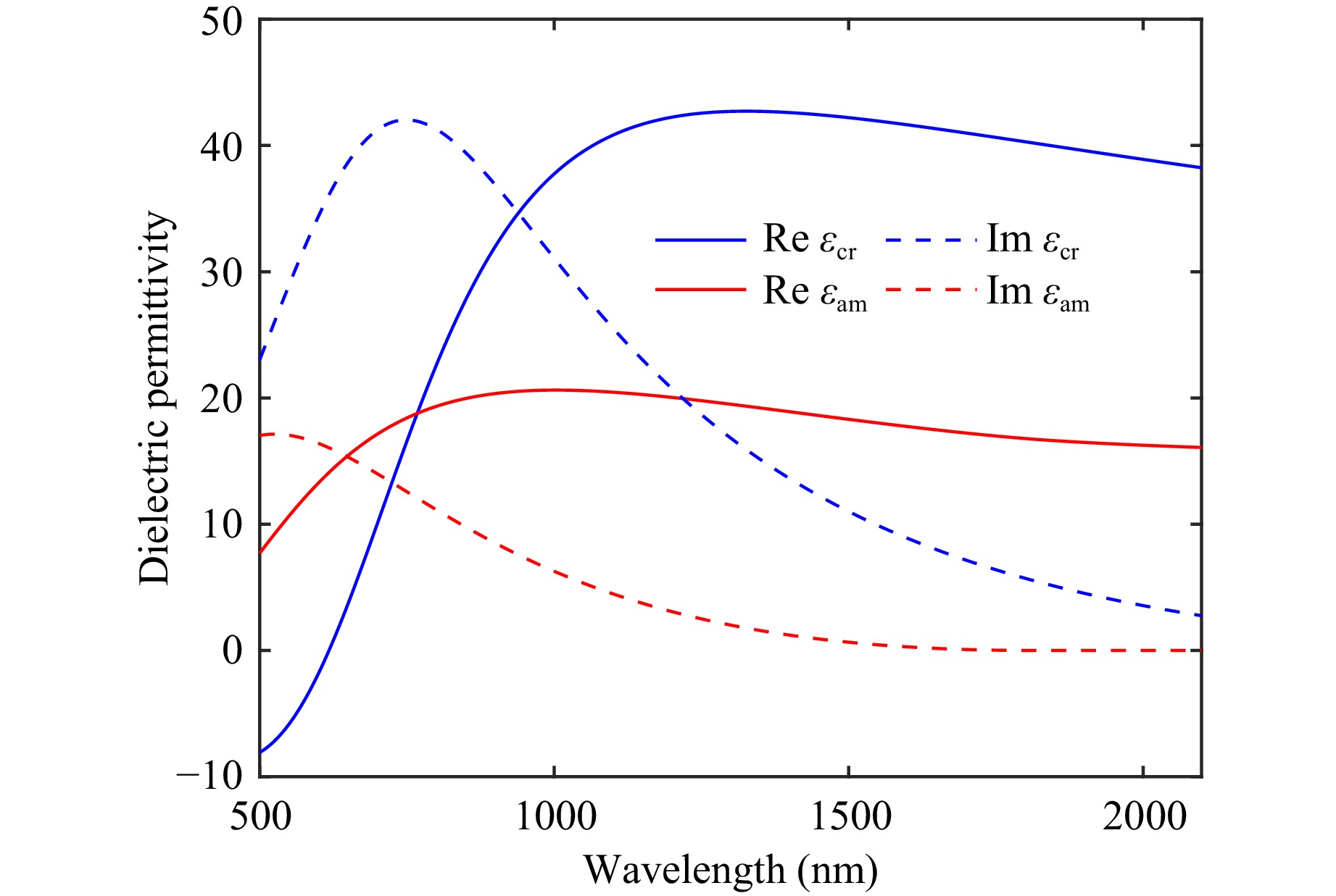
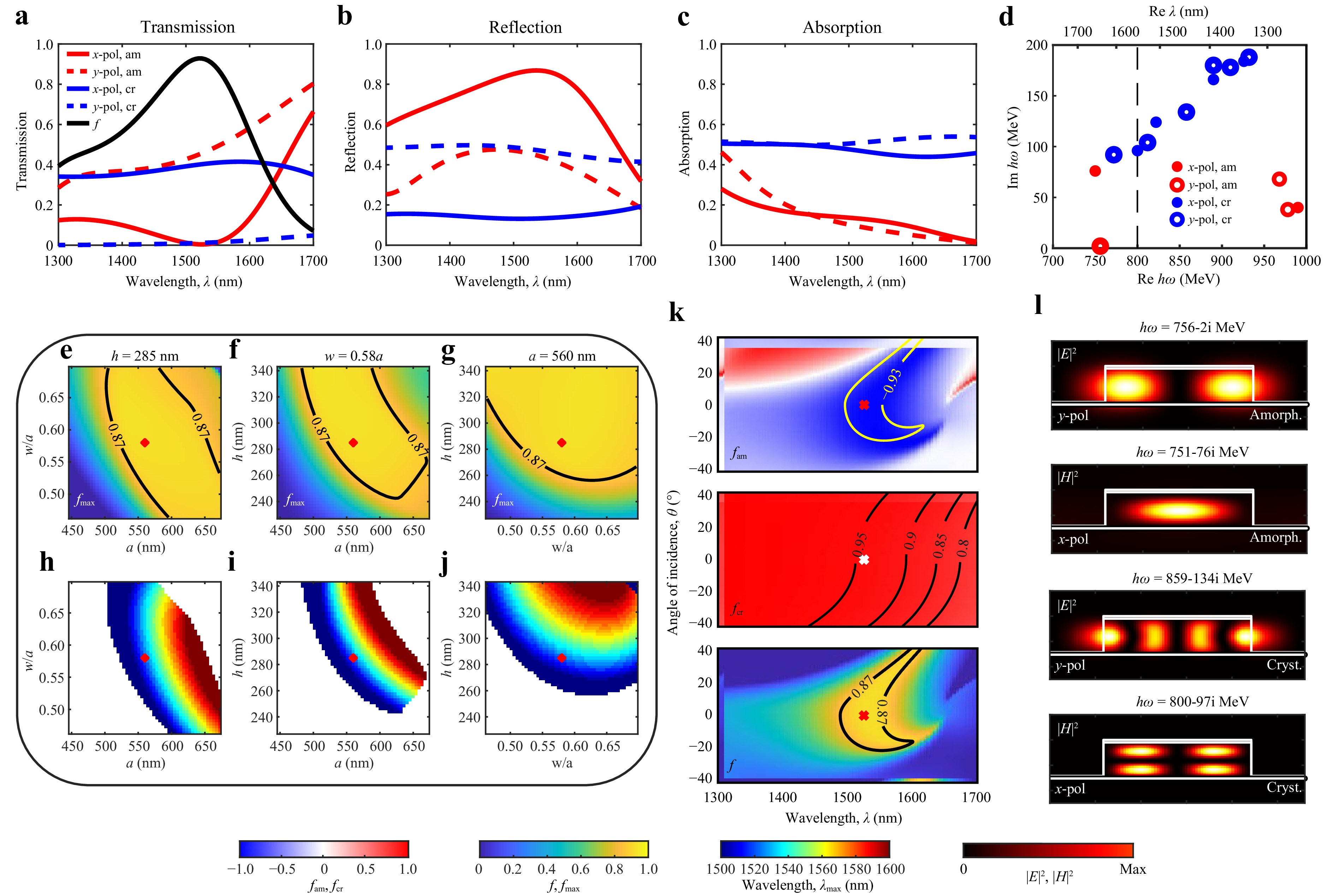
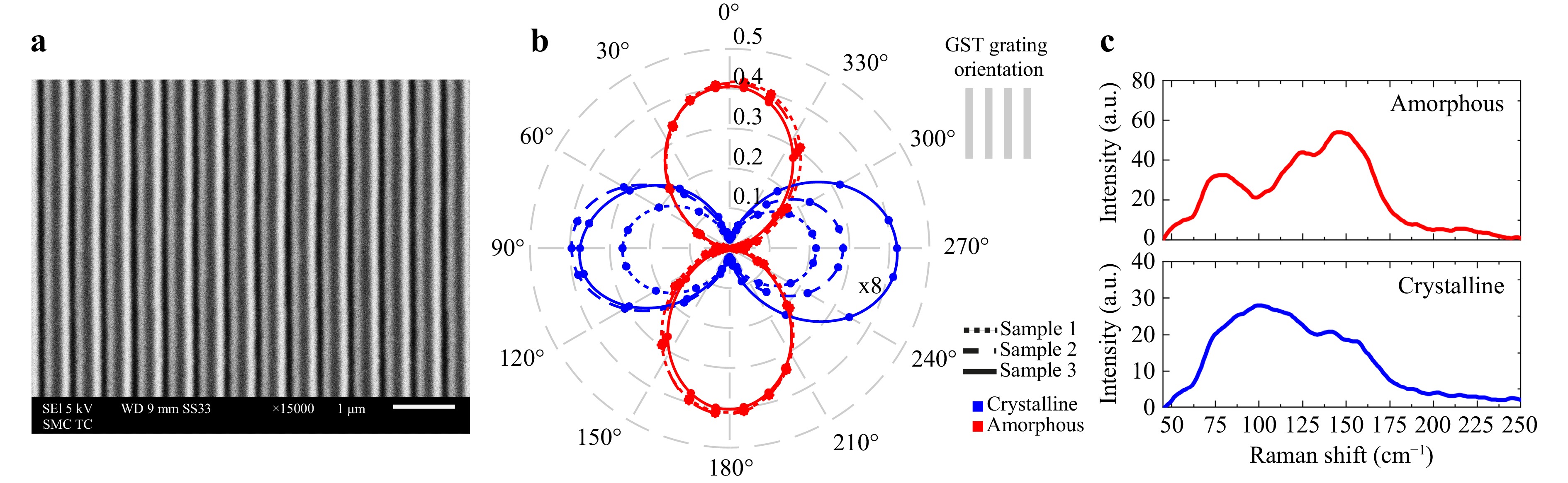
Wire-grid polarizers, which consist of a one-dimensional periodic metasurface, are convenient polarising elements used in many optical applications. However, these metasurfaces are still incapable of switching the polarisation state of transmitted light without mechanical rotation. This article presents the design of a switchable wire-grid polariser based on a one-dimensional metasurface composed of the phase-change material Ge-Sb-Te (GST). Using the Fourier modal method and genetic-algorithm-based optimisation, we designed a metasurface that transmits two orthogonal linear polarisations of light in different phase states. We demonstrate that the designed metasurface is stable with respect to variations in wavelength and angle of incidence, as well as variations in the geometrical parameters of the metasurface. This concept was verified by measuring the transmission characteristics of a GST metasurface fabricated using magnetron sputtering on a glass substrate. The experimental extinction ratio of the fabricated samples in both polarisation states ranged between 10 and 14~dB, depending on the specific sample. Because the phase transition in GST films can occur on a sub-microsecond timescale, the developed switchable wire-grid polariser offers significant potential for creating a fast, compact polarisation modulator for telecommunication wavelengths.
Published. 2026, 7(3)
: 913-924
doi: 10.37188/lam.2026.087
Ultrathin (\begin{document}$ \phi $\end{document} \begin{document}$\phi $\end{document}
Design-for-manufacture, fabrication, and assembly of an all-reflective freeform microscope objective
Published. 2026, 7(3)
: 925-937
doi: 10.37188/lam.2026.113
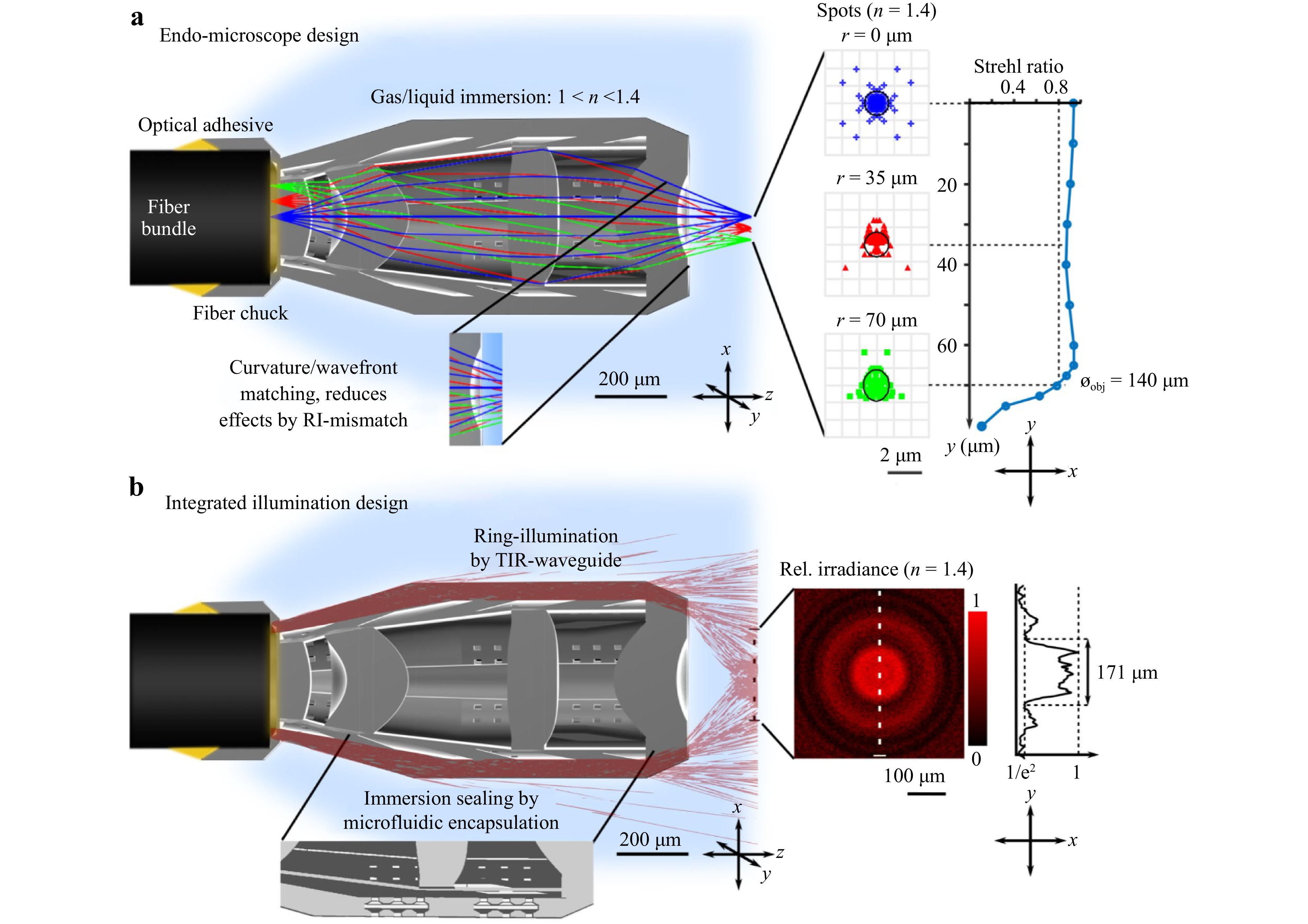
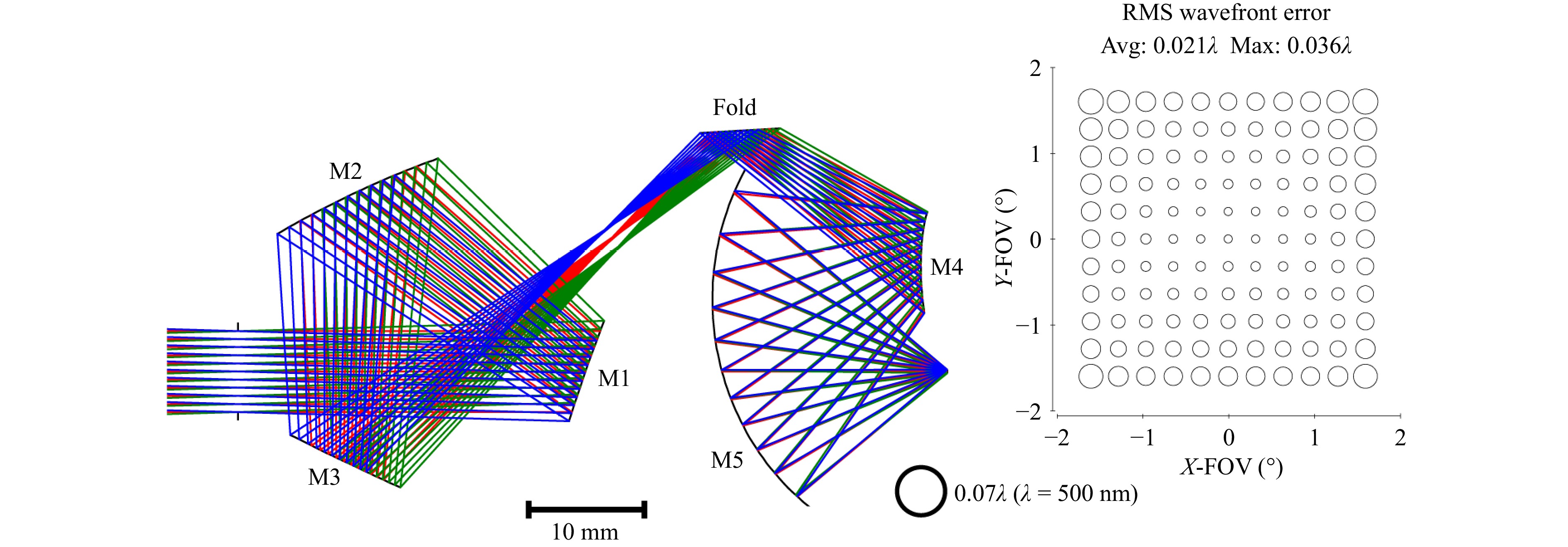
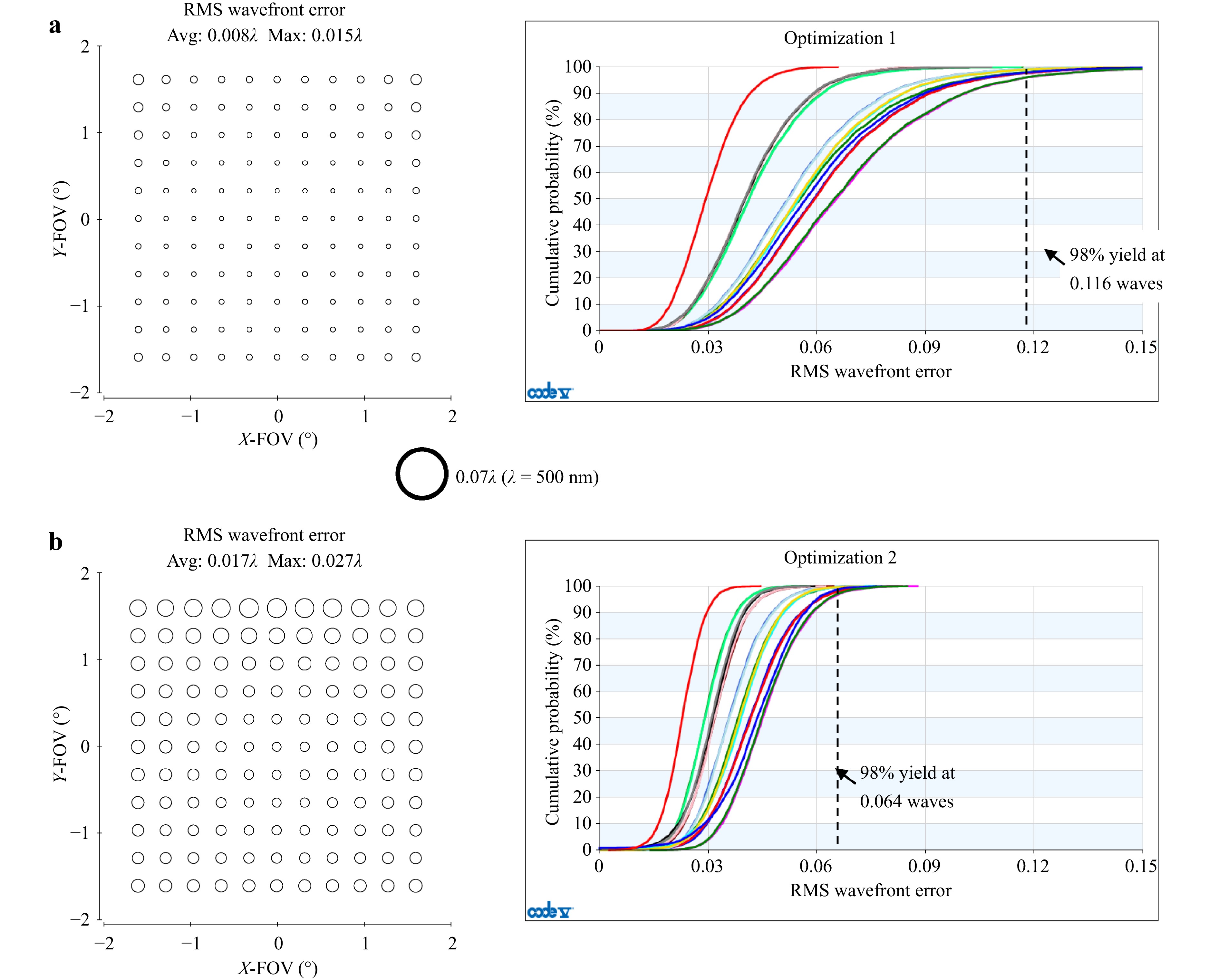
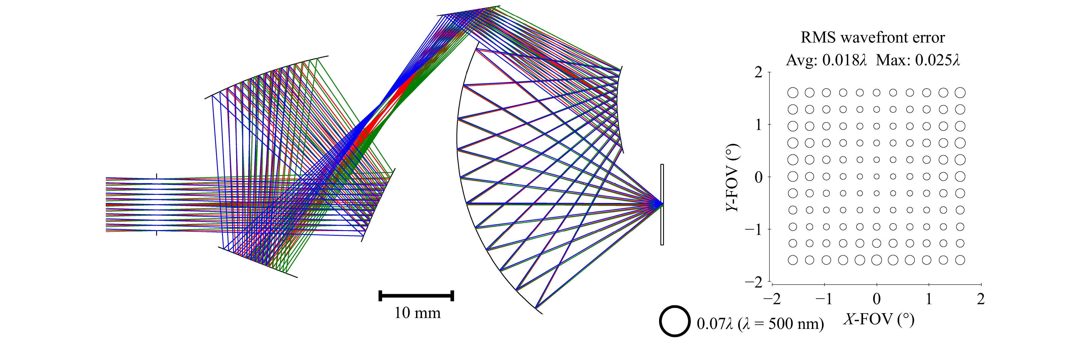
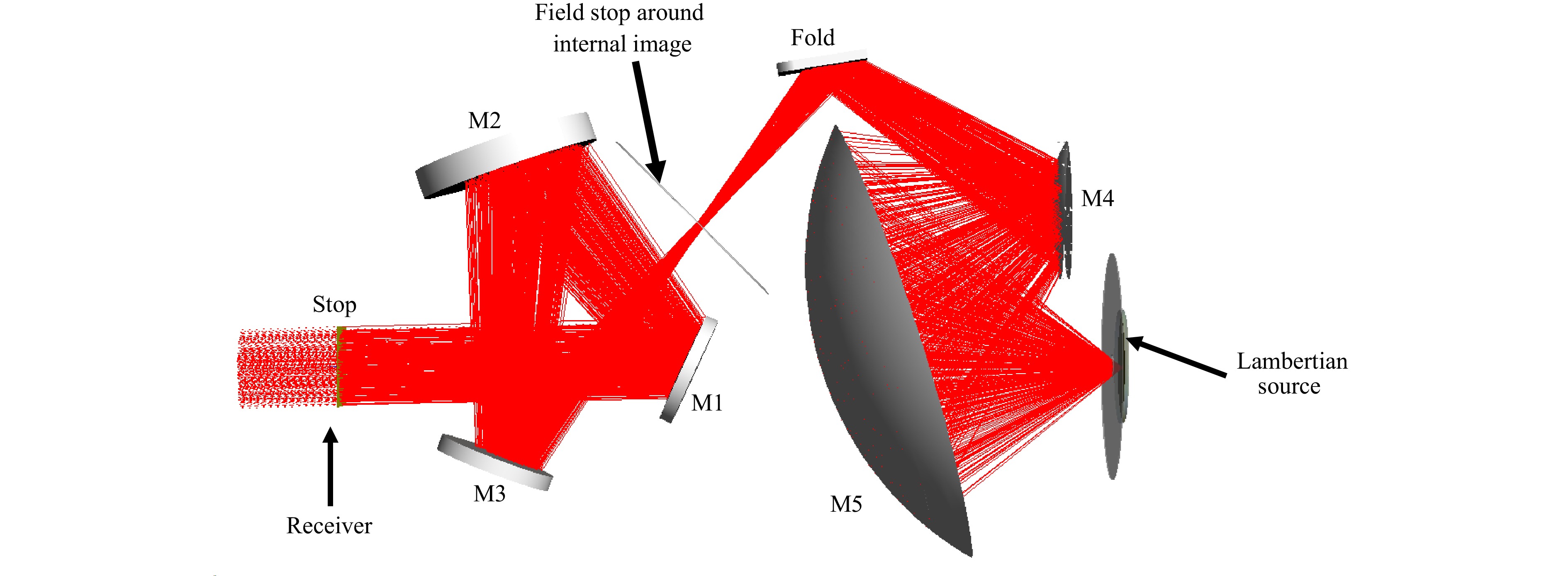
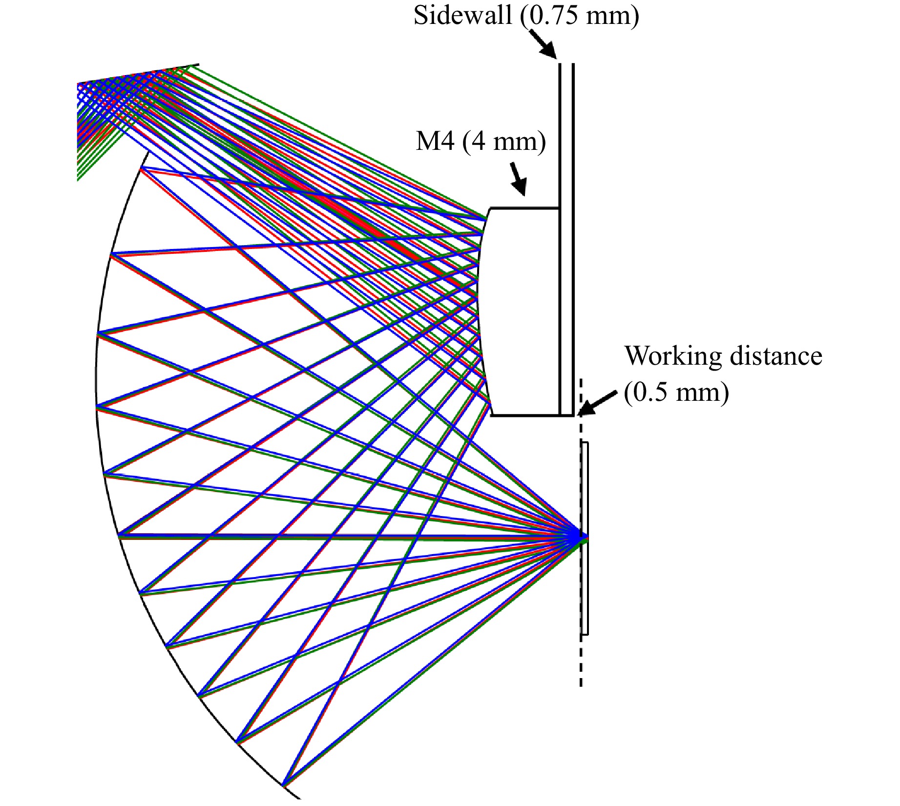
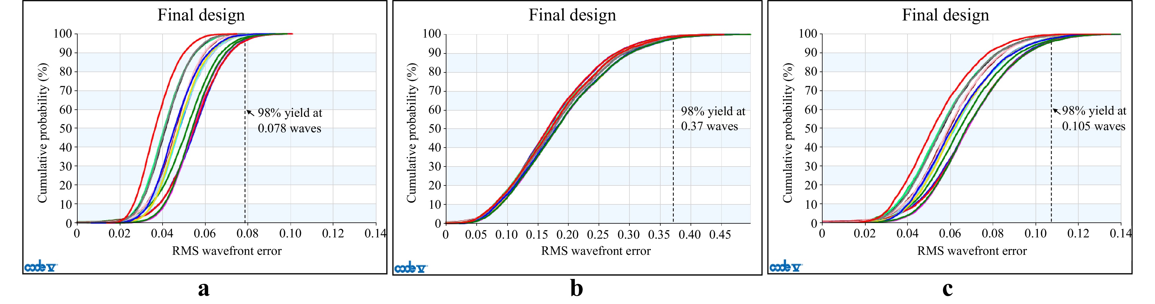
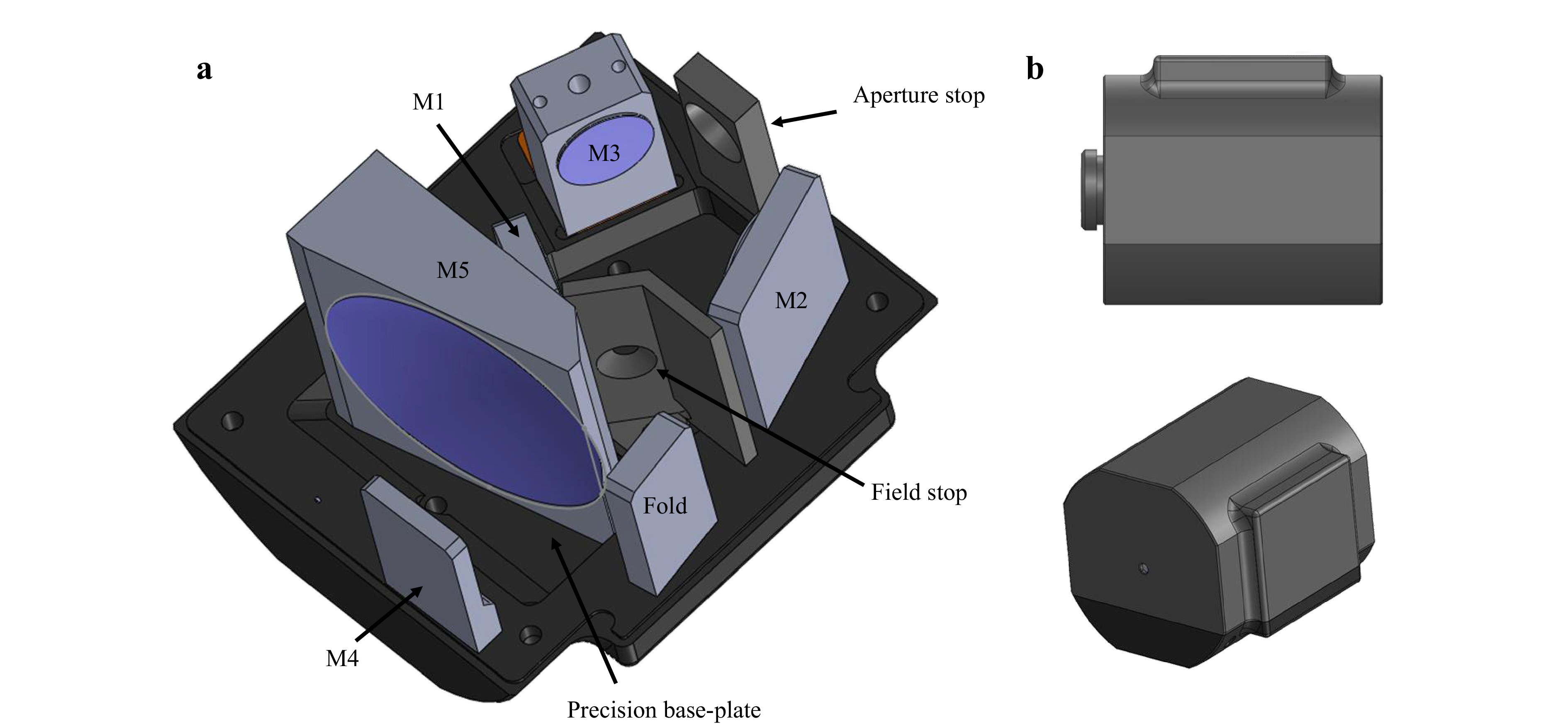
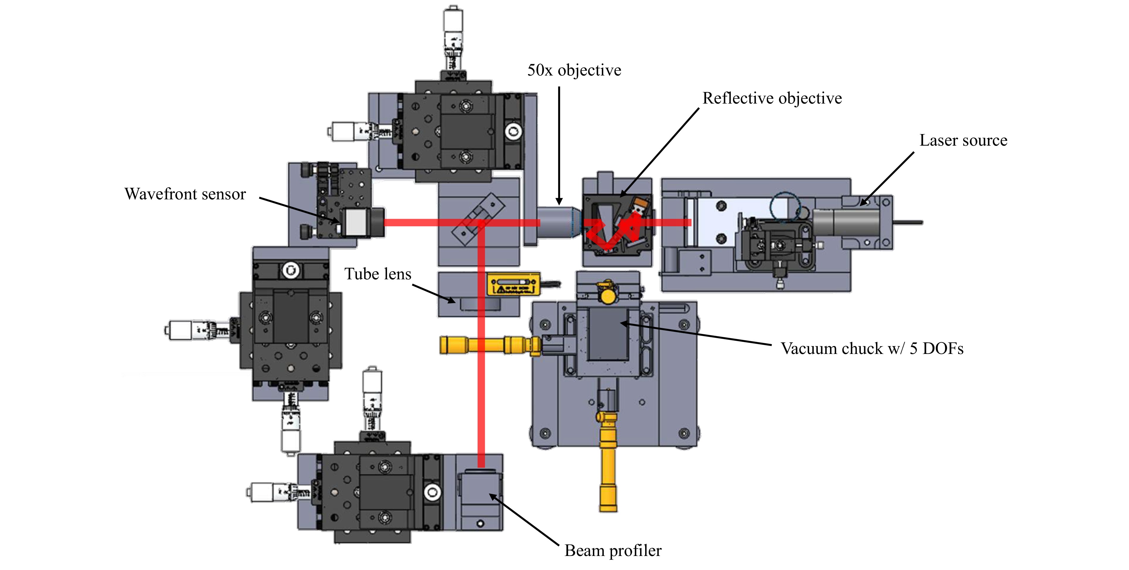
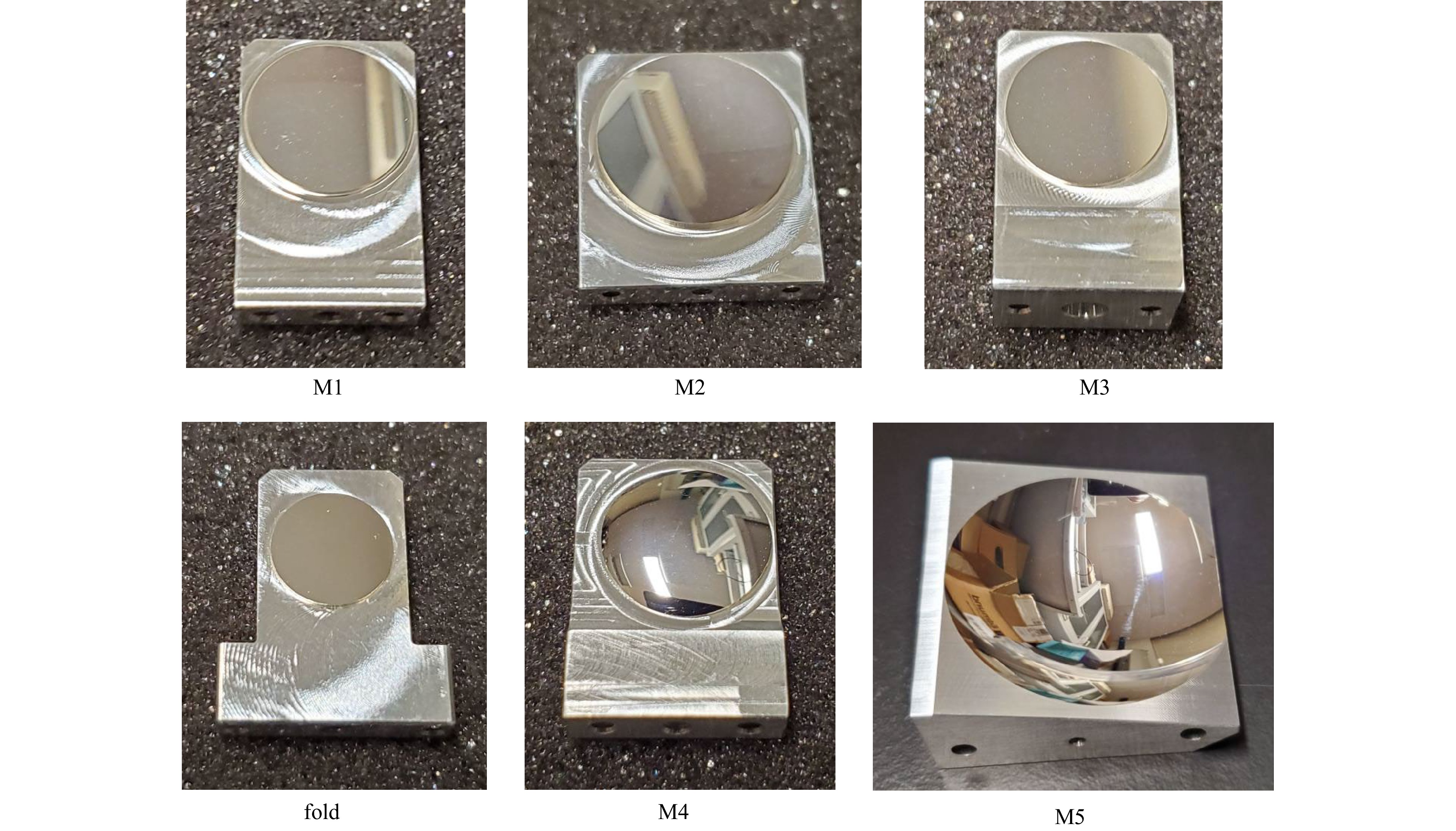
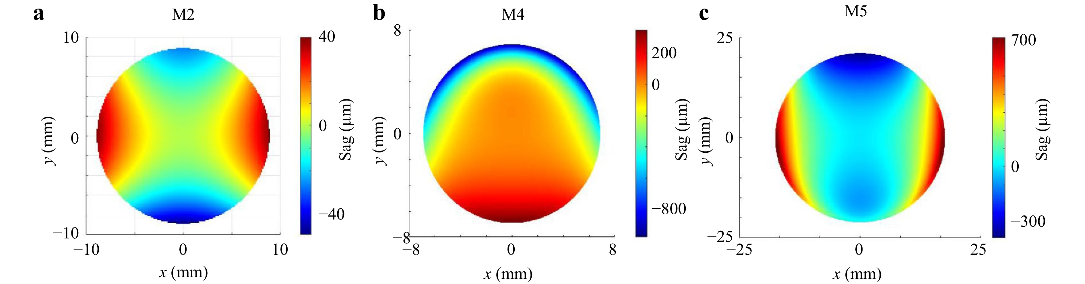
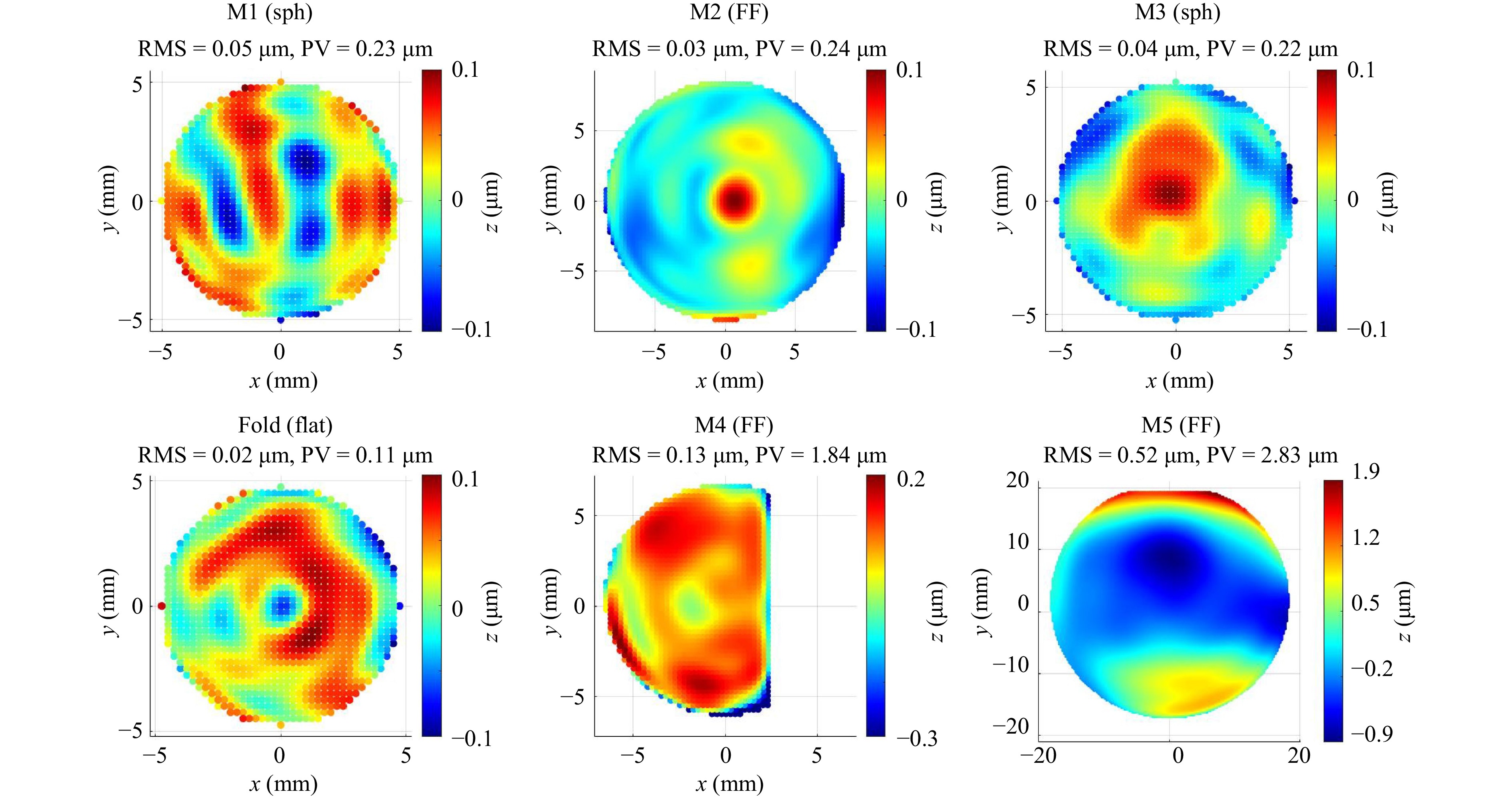
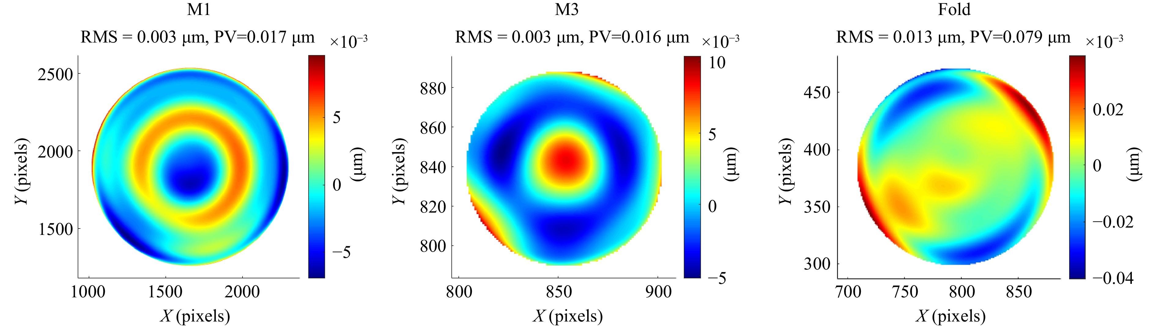
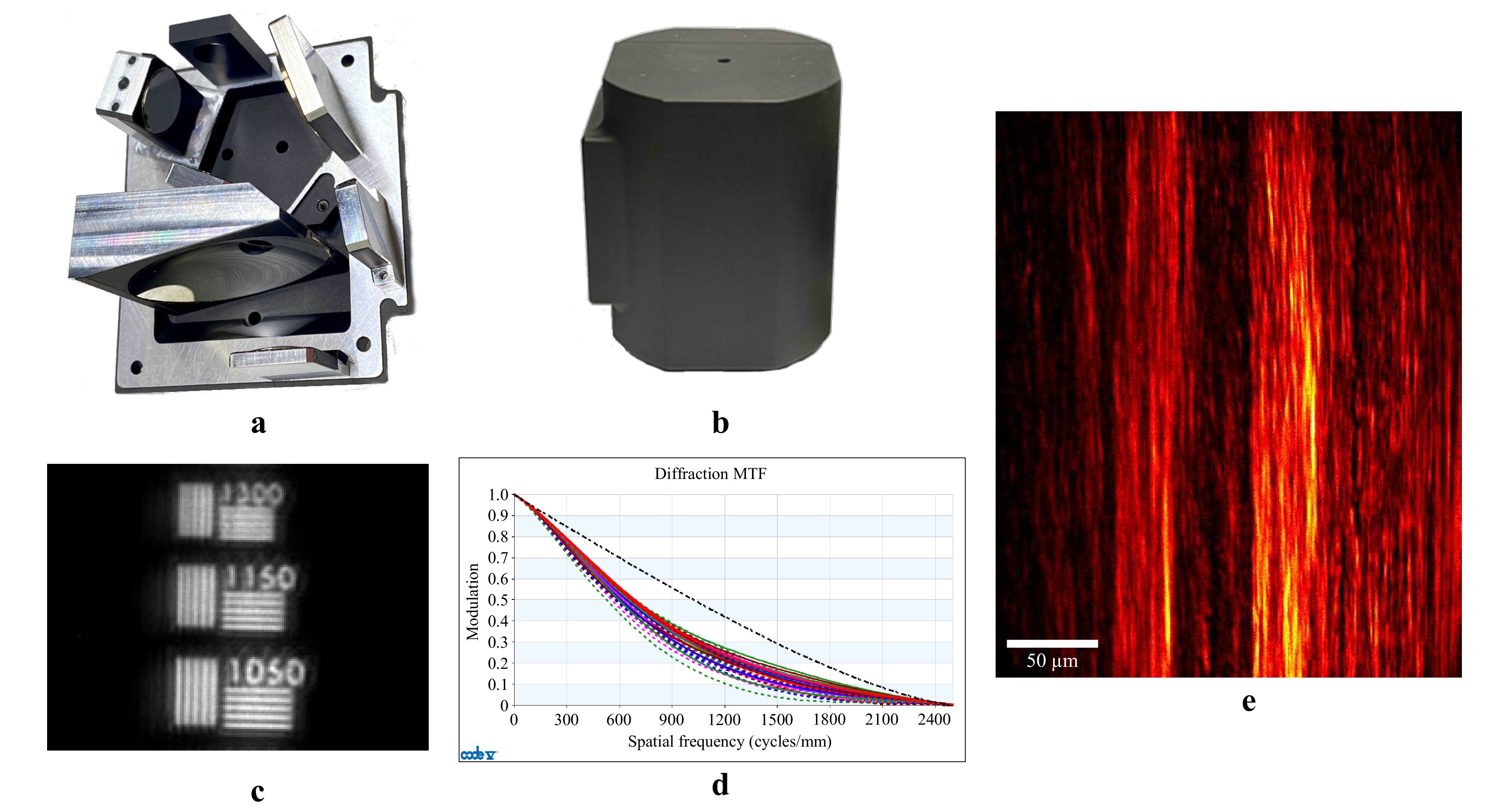
All-reflective microscope objectives offer distinct advantages for microscopy techniques that operate across widely separated spectral bands. However, designing a high numerical-aperture (NA), unobscured, all-reflective objective that is manufacturable remains a substantial challenge, requiring early integration of fabrication considerations into the optical design process. In this work, we present design-for-manufacture strategies for a 0.65-NA unobscured all-reflective microscope objective enabled by freeform optics. These strategies include minimizing freeform departures, desensitization optimization, and a stray-light analysis. Concepts for mounting and assembly are also introduced and implemented, culminating in the successful fabrication and imaging demonstration of the first system of its kind.
Published. 2026, 7(3)
: 938-951
doi: 10.37188/lam.2026.093
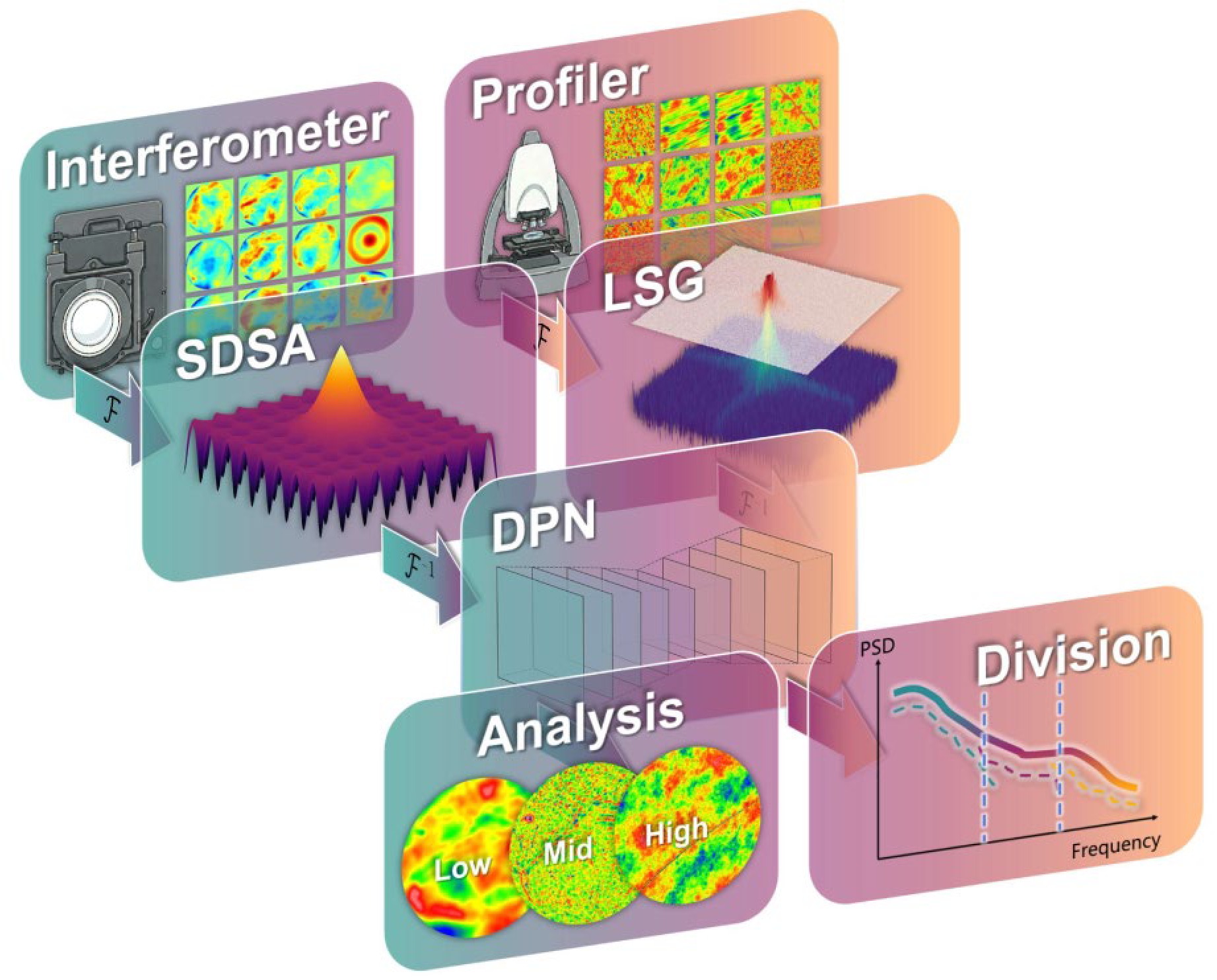
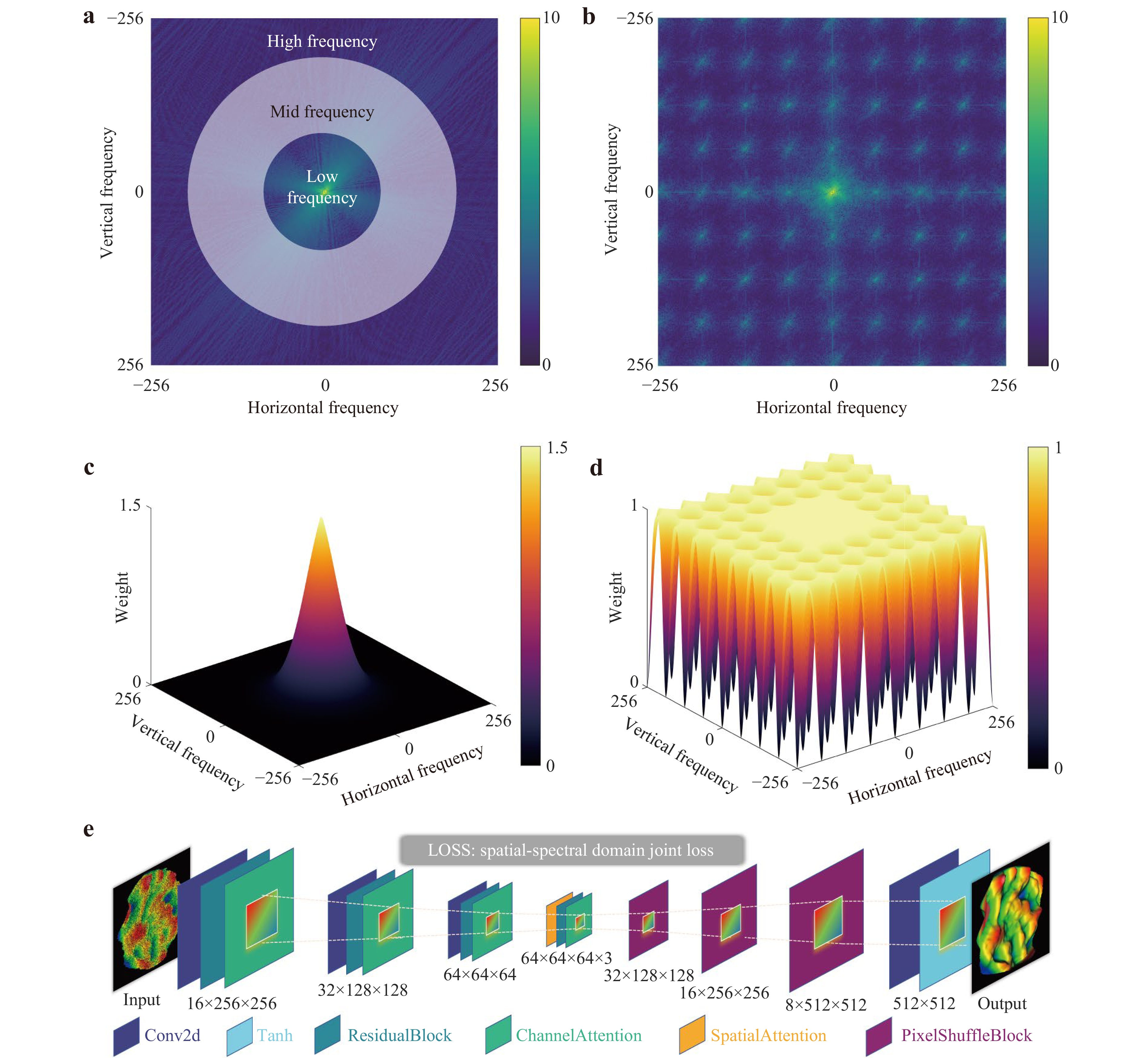
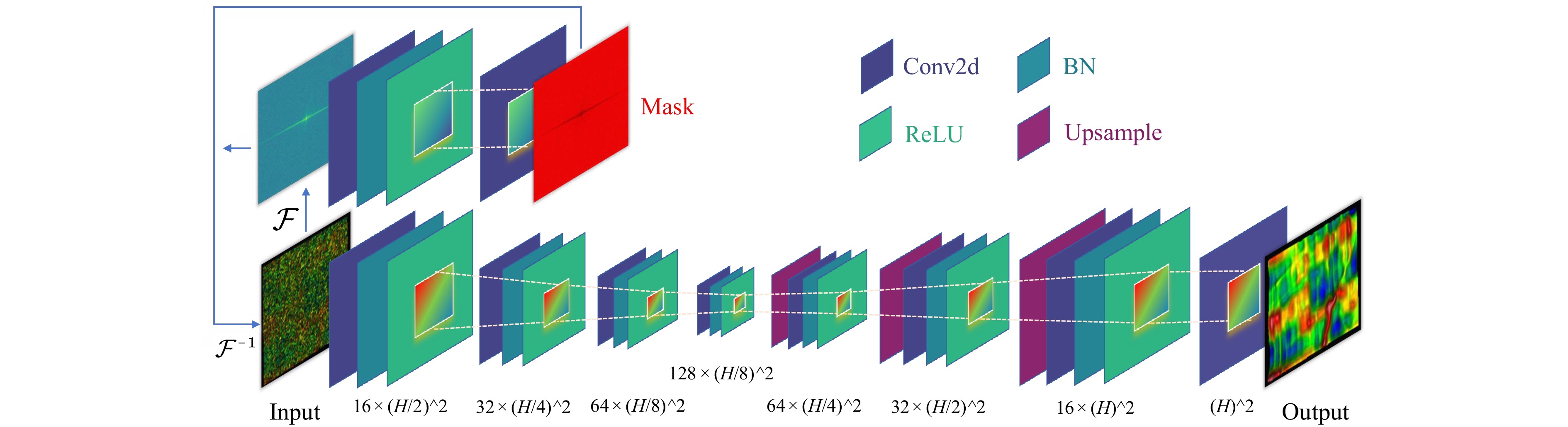
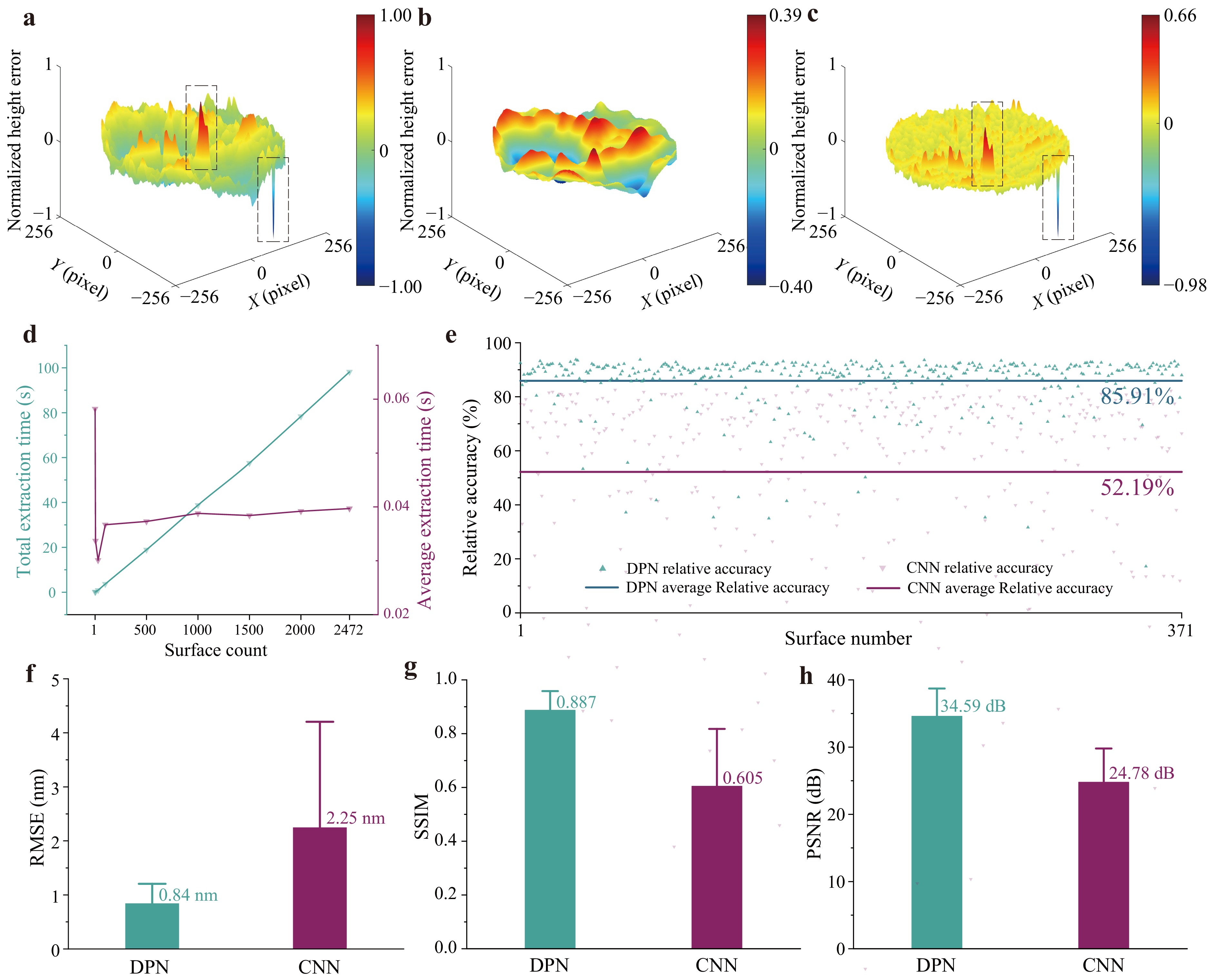
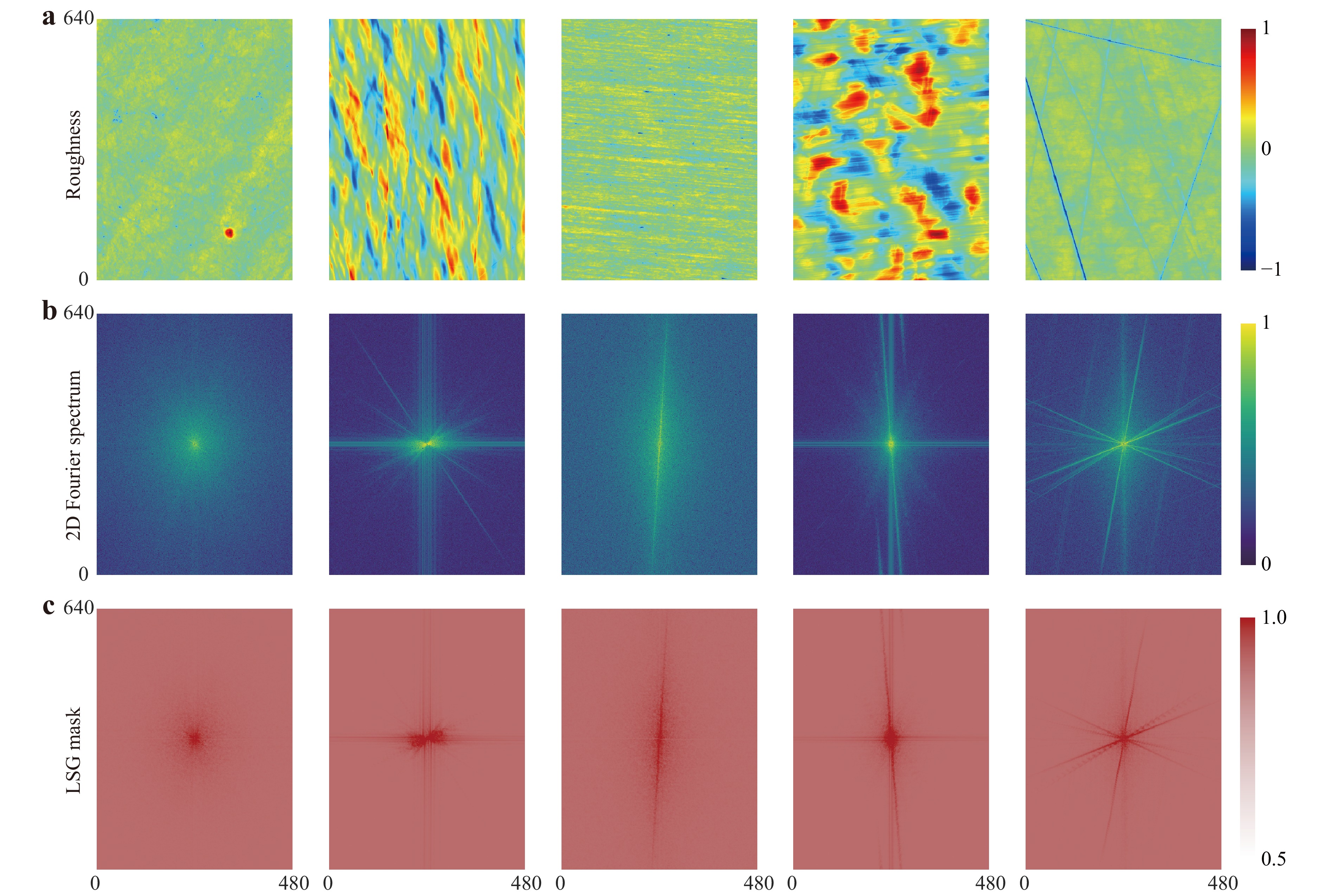
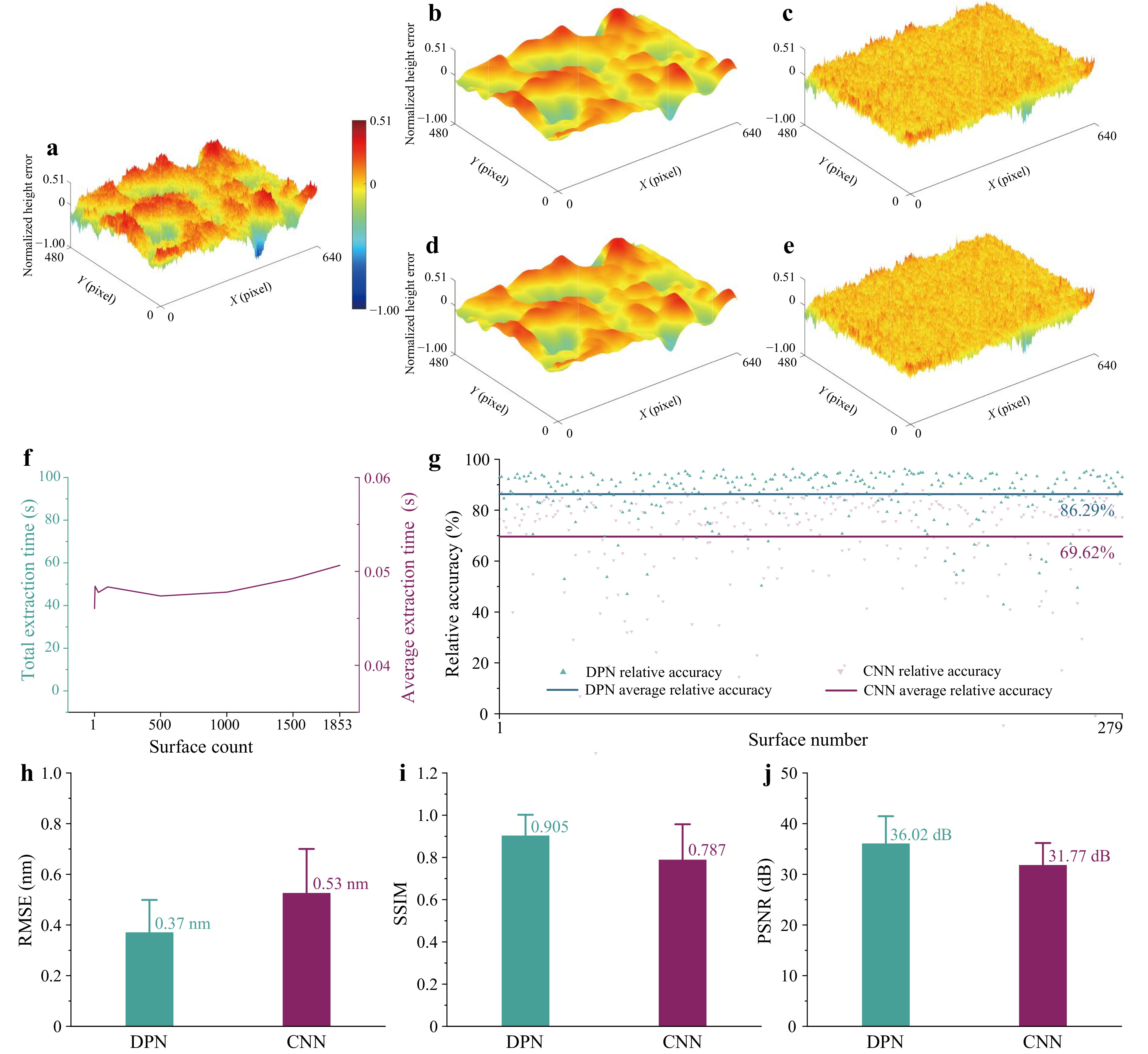
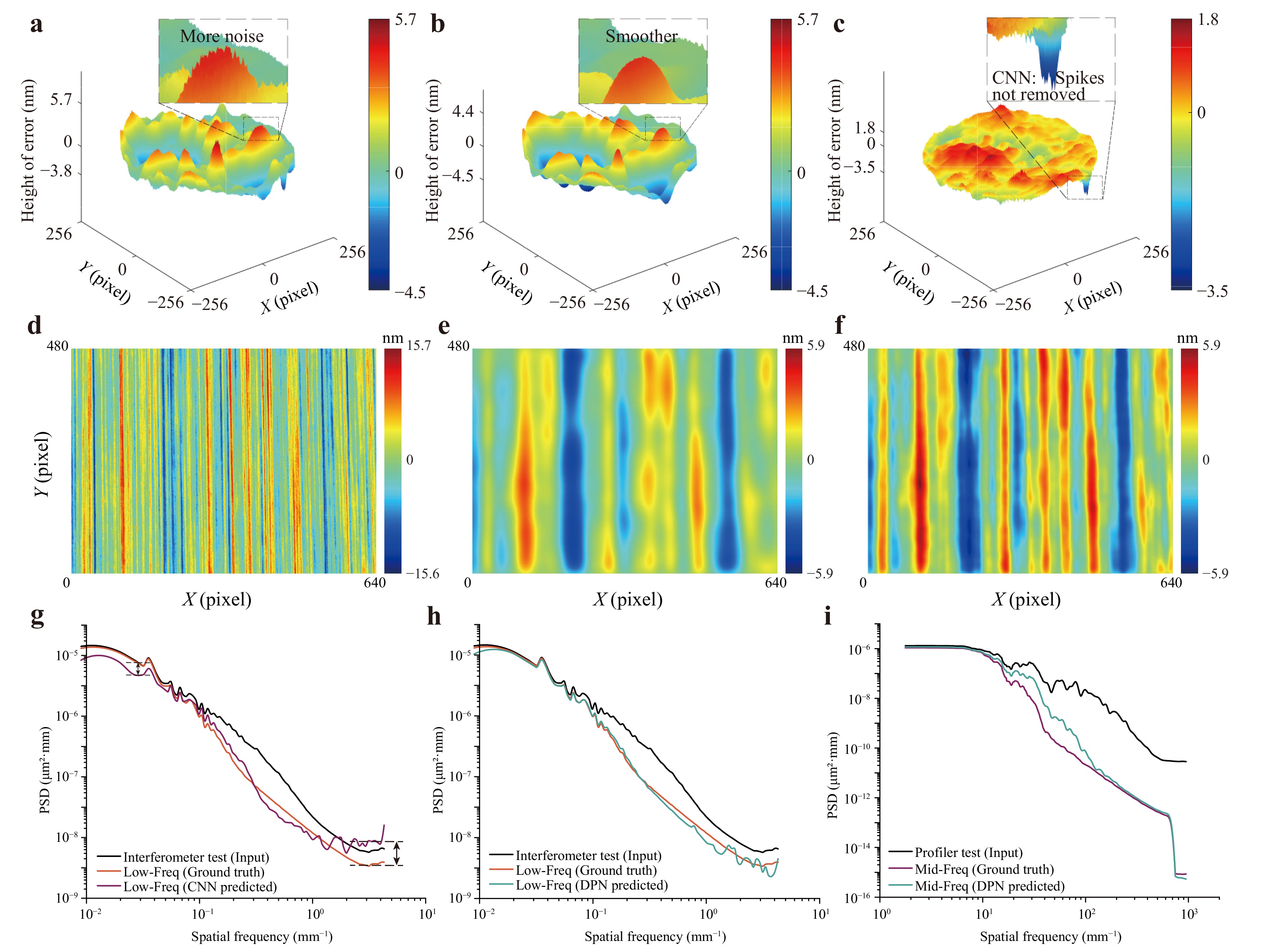
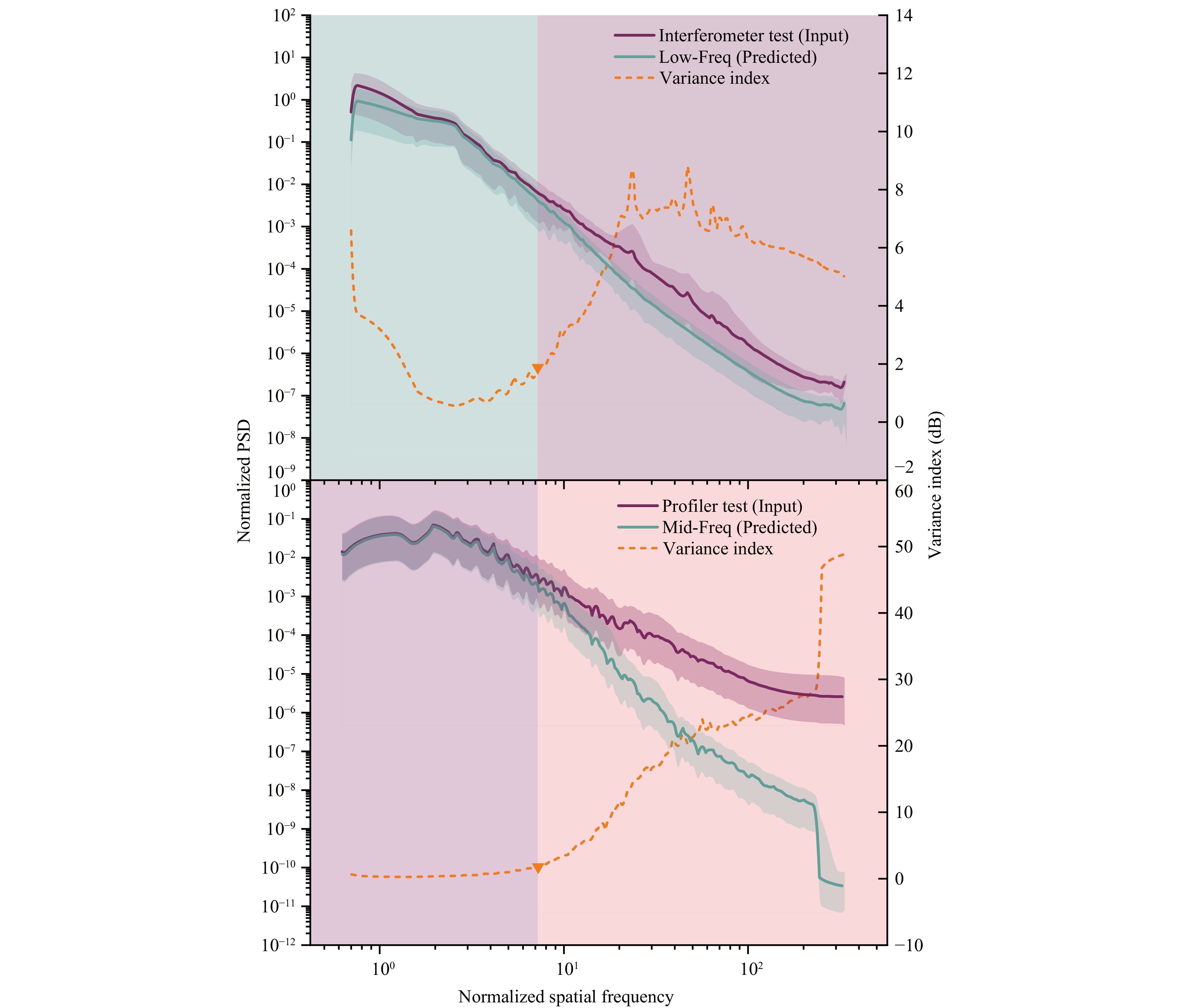
Precisely separating full-band surface errors is a cornerstone of high-performance optical manufacturing and testing. However, traditional methods rely on subjective frequency band definitions and manual filtering, which leads to inconsistent evaluation standards and introduces analysis errors. Meanwhile, existing data-driven methods mechanically fit noisy manual labels, lacking physical consistency. To address this issue, this paper presents a scale-adaptive physics-aware deep learning framework powered by a dual-domain physics-aware network, which extracts error features by imposing physical constraints in the frequency domain: a specifically shaped spectral domain selective attention mechanism is designed for a low-frequency error with a deterministic spectral envelope; an adaptive learnable spectral gating is designed for mid-frequency error with randomness and anisotropy. Experiments indicate that this network outperforms conventional models under adopted evaluation metrics and exhibits physics-constrained extraction behaviour. This helps mitigate measurement noise and subjective variability introduced by manual filtering, yielding results with improved spectral and physical consistency. Furthermore, it eliminates the reliance on high-performance computing hardware, thereby enabling millisecond-level real-time inference on a standard computer, which greatly facilitates practical engineering deployment. Based on these findings, this study proposes a generalised frequency band division method based on normalised spatial frequency, providing a normalised-frequency-based method for a more consistent cross-scale and cross-instrument frequency band error division.
Published. 2026, 7(3)
: 952-961
doi: 10.37188/lam.2026.102
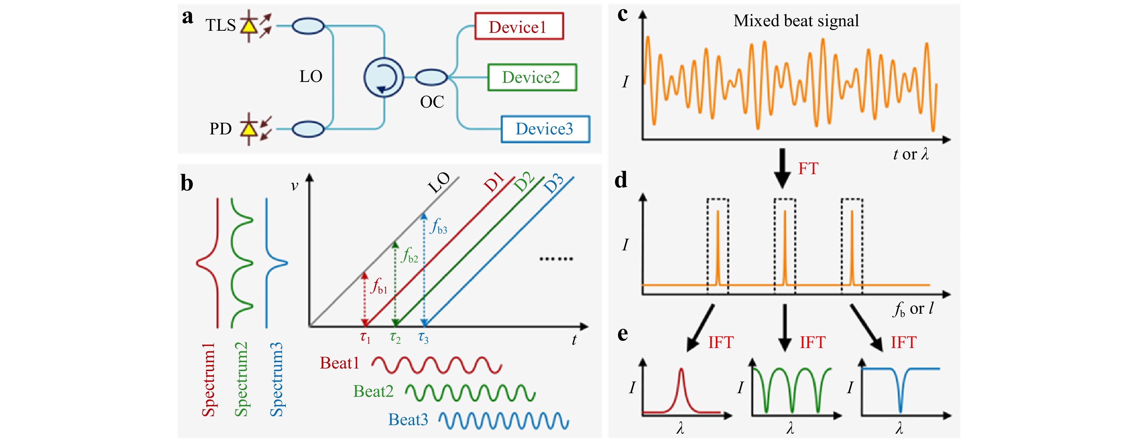
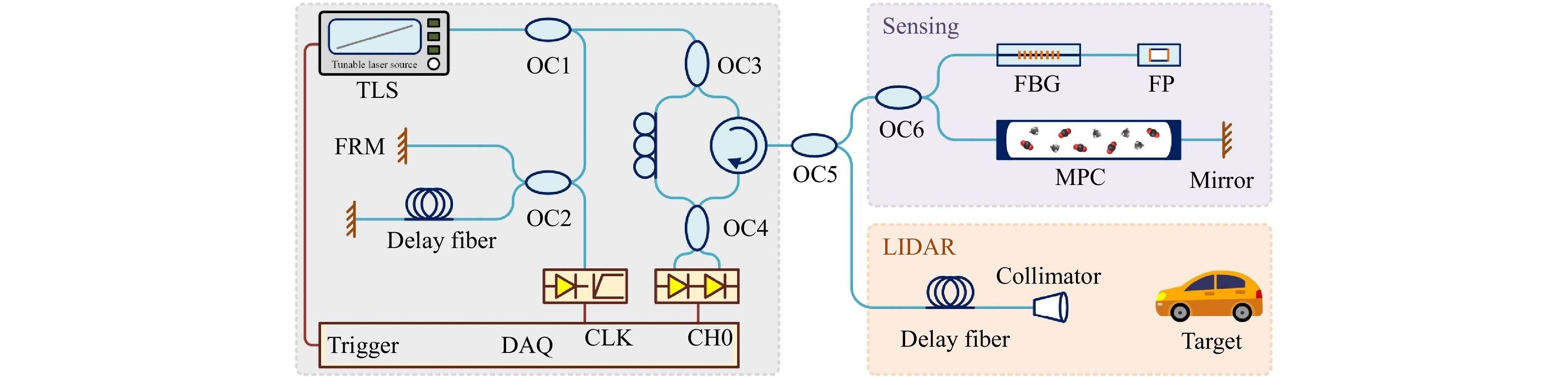
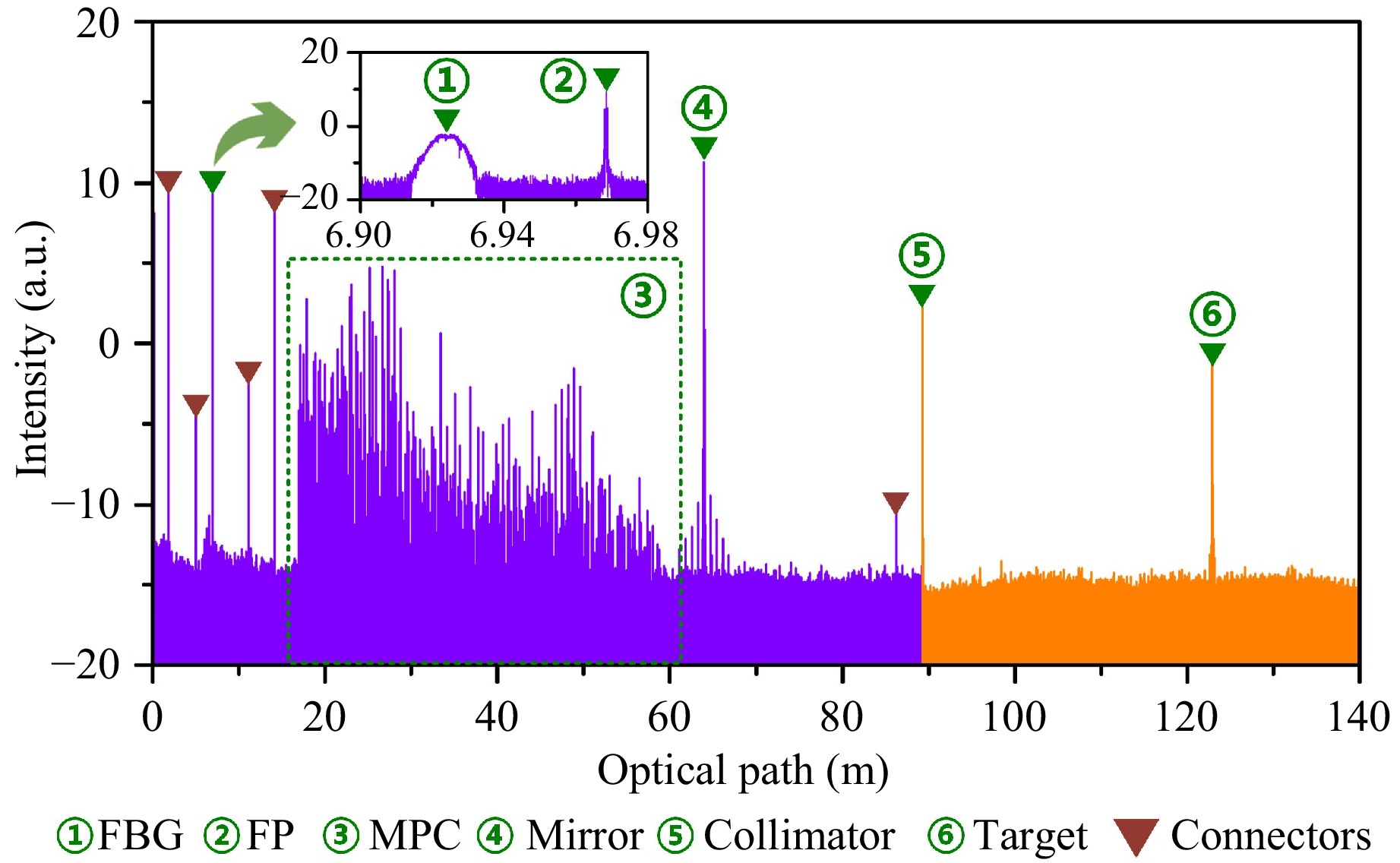
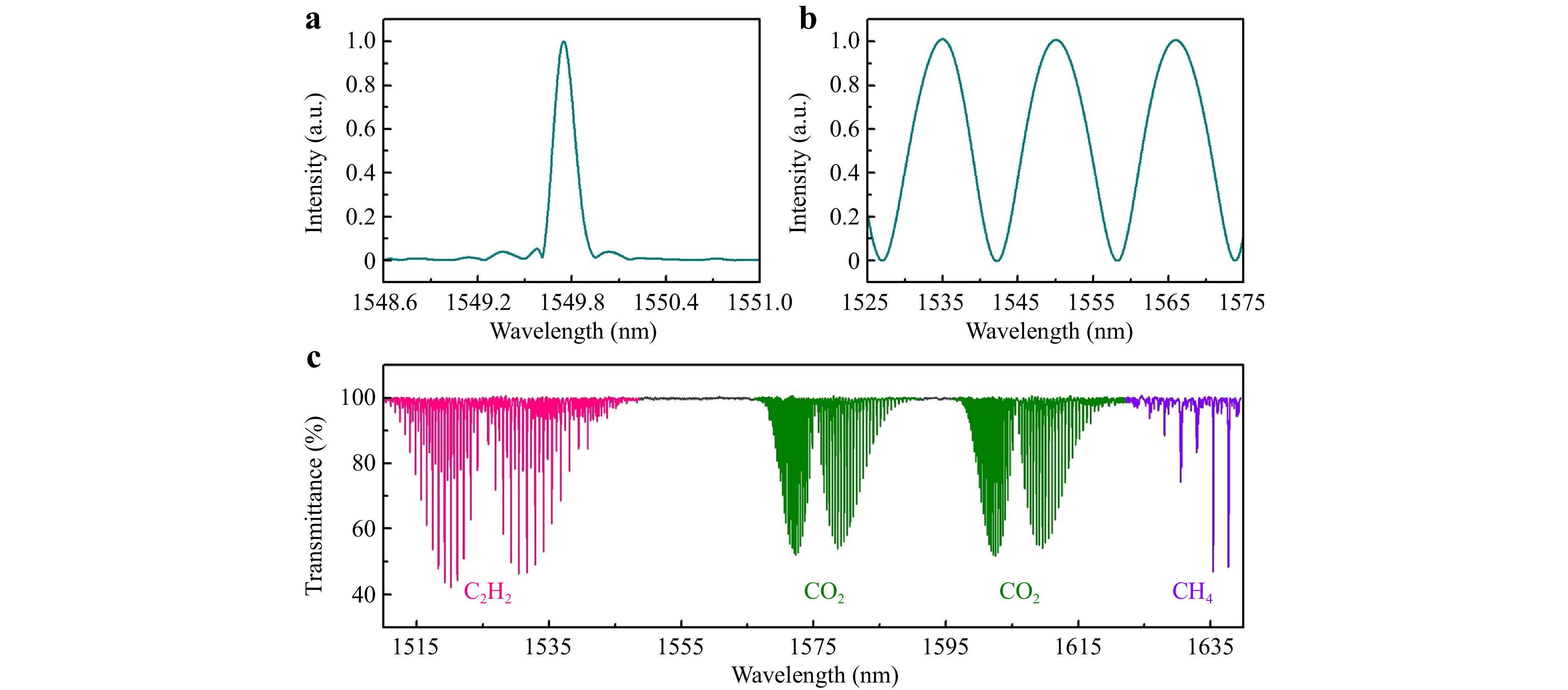
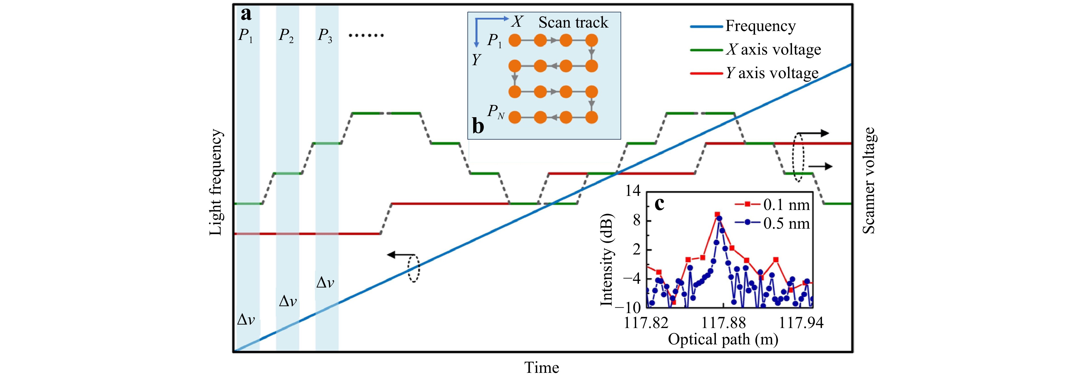
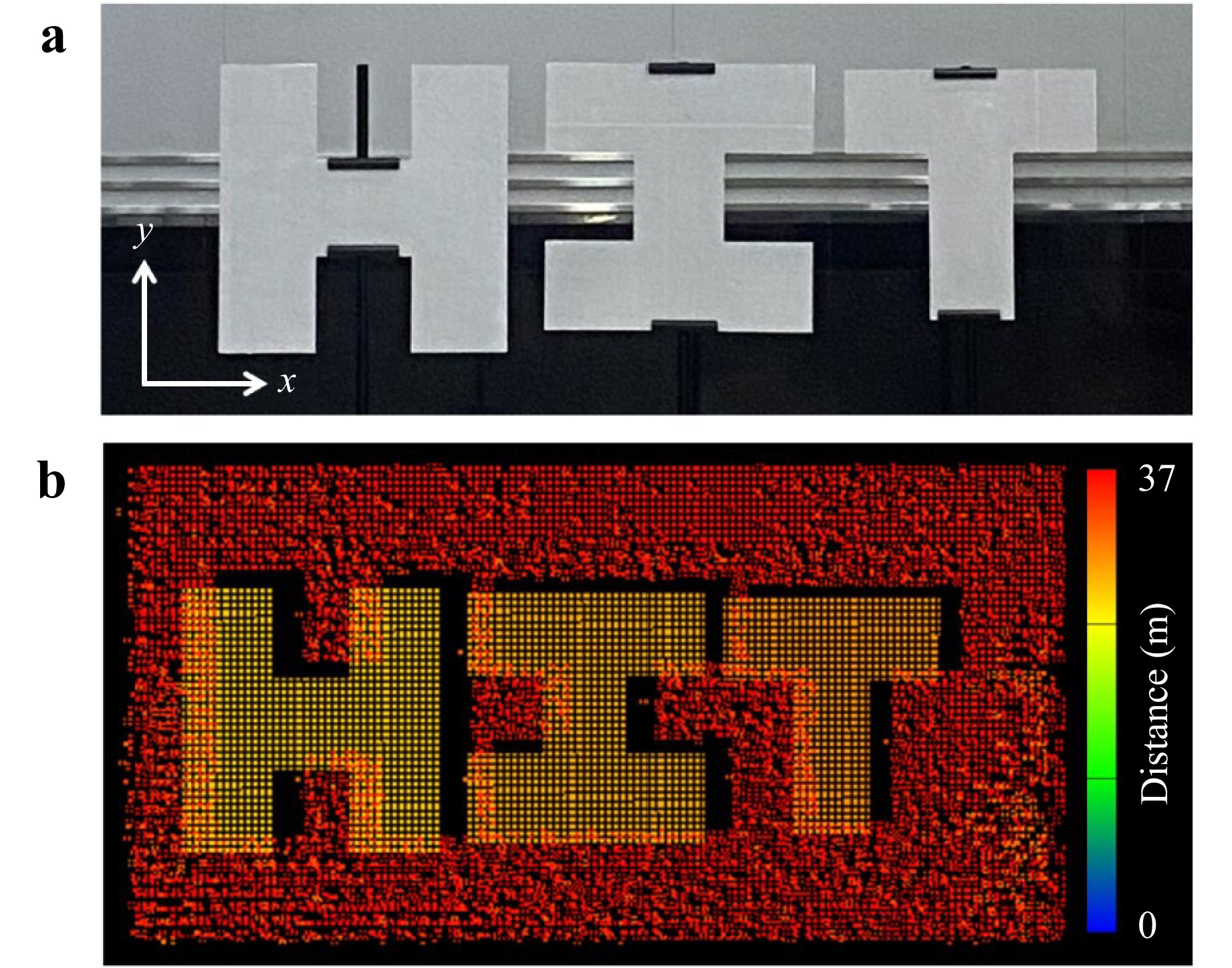
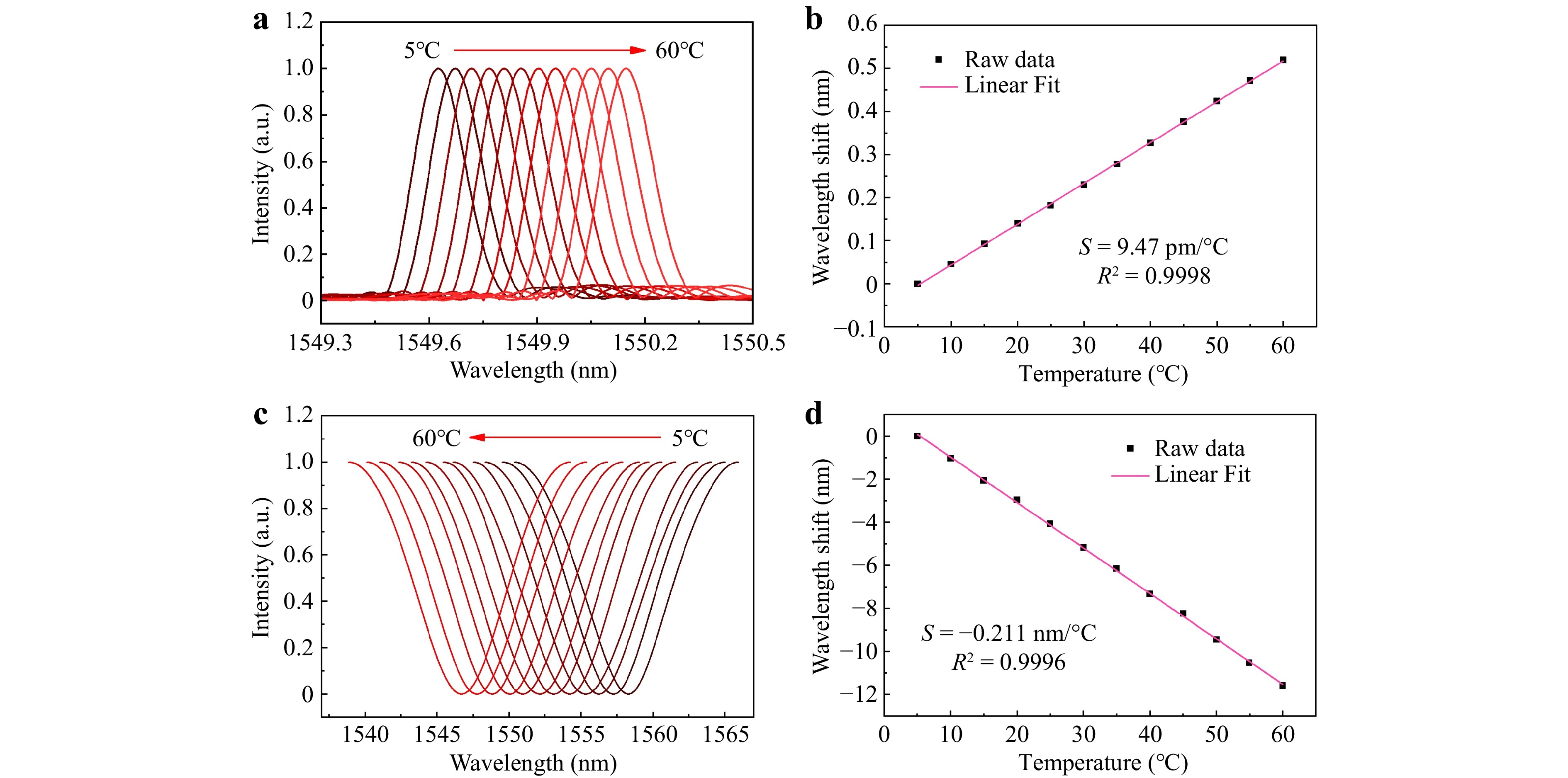
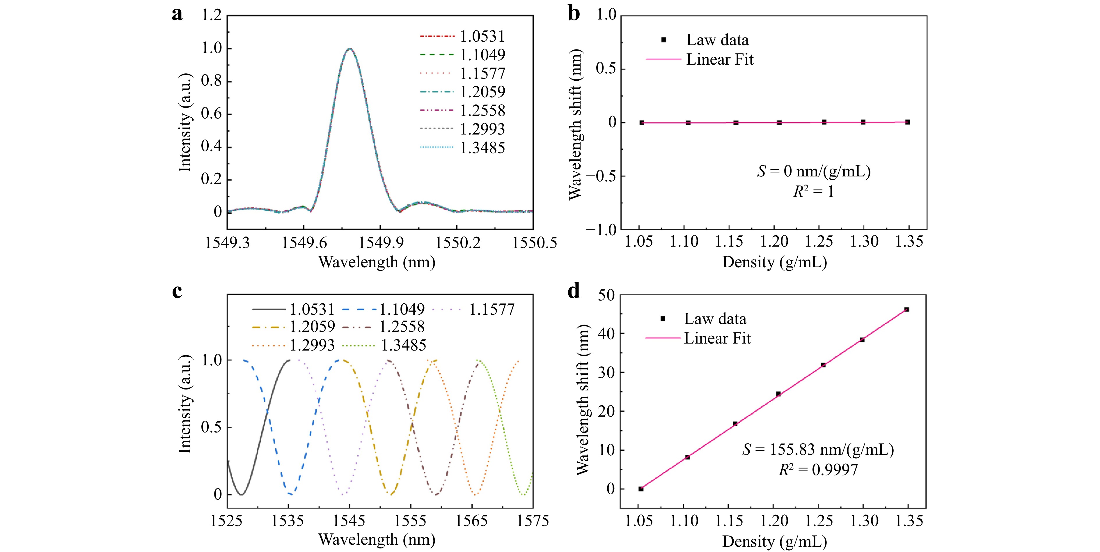
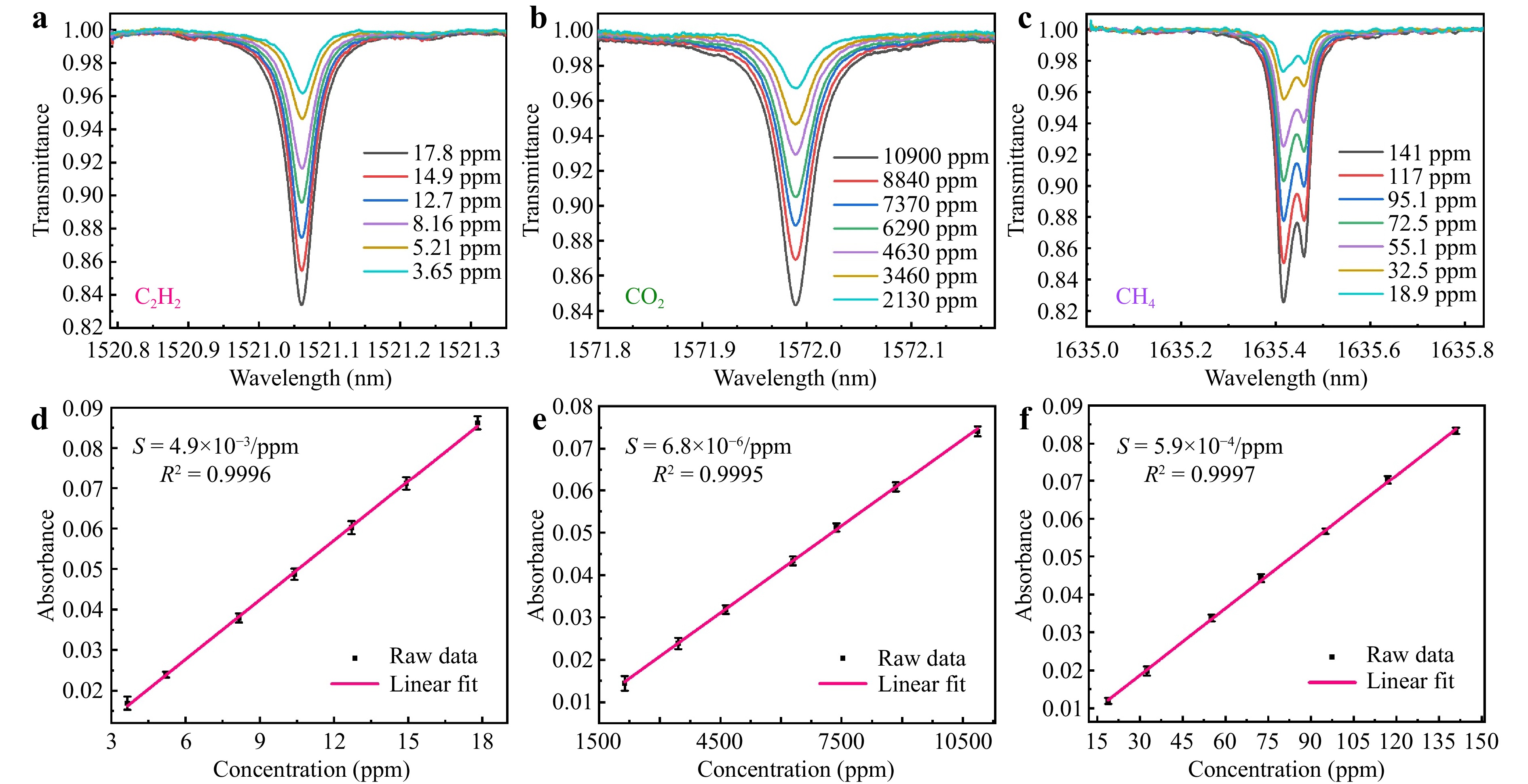
Traditional frequency-modulated continuous-wave (FMCW) light detection and ranging (LiDAR) is primarily used for high-precision distance measurements in free space. In this paper, a multifunctional FMCW LiDAR capable of high-precision ranging and multi-parameter sensing is proposed. By detecting echo signals from both free space and optical fibres, 3D imaging and the measurements of diverse physical parameters, including environmental temperature, gas concentrations, and liquid density, can be measured simultaneously. In an experiment, a target at 30 m was imaged with an adjustable resolution spanning 0.3–1.2 cm. Meanwhile, the electrolyte density and temperature of a battery were measured with accuracies of 3×10⁻⁵ g/mL and 0.5 °C, respectively. The concentrations of the gases (C2H2, CO2, and CH4), which are critical for monitoring thermal runaway of a battery, were measured with detection limits of 0.07, 48, and 0.56 ppm, respectively. The proposed multifunctional LiDAR exhibits significant application potential in fields such as new-energy vehicles and spacecraft.
Published. 2026, 7(3)
: 962-970
doi: 10.37188/lam.2026.091
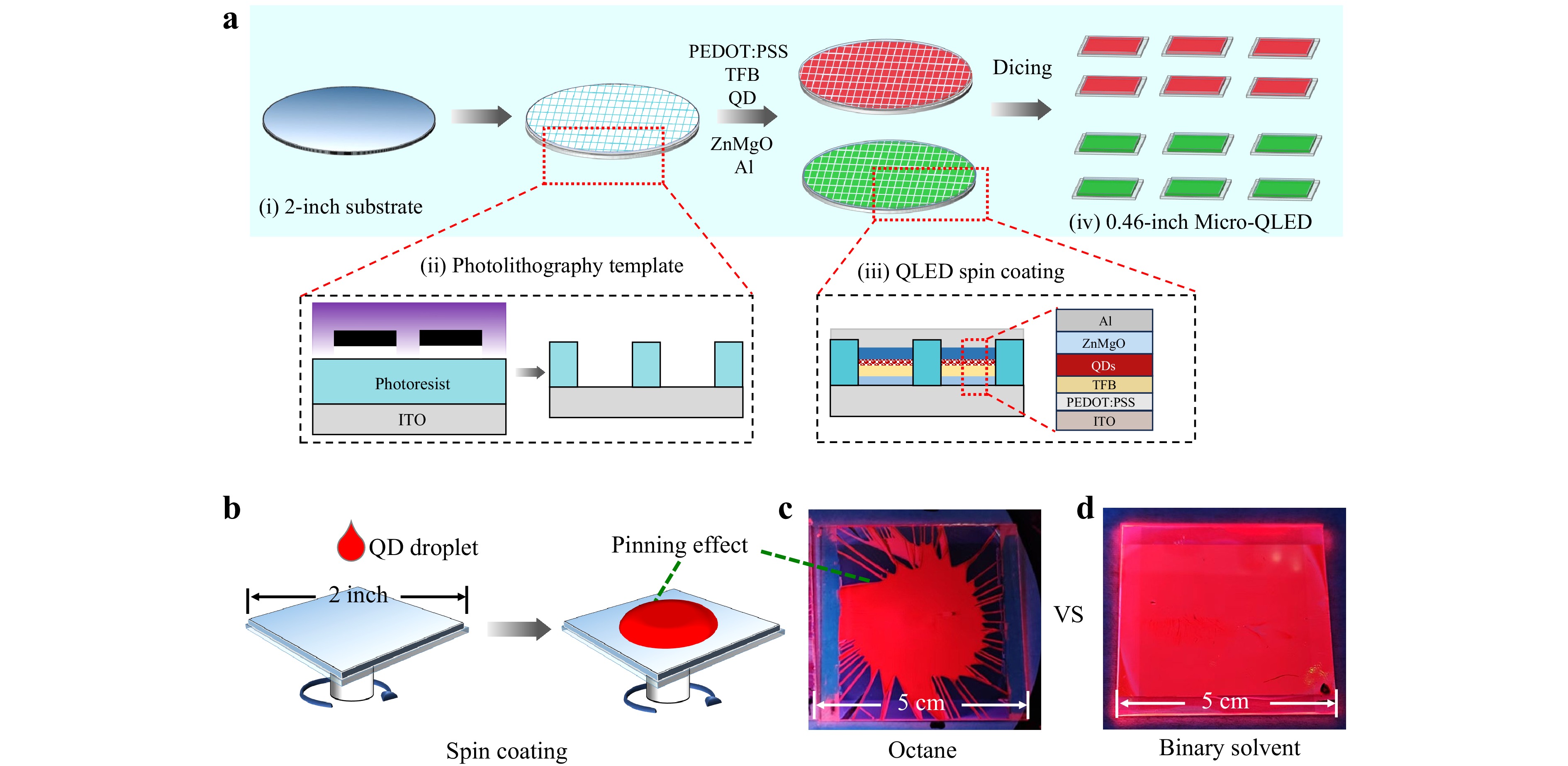
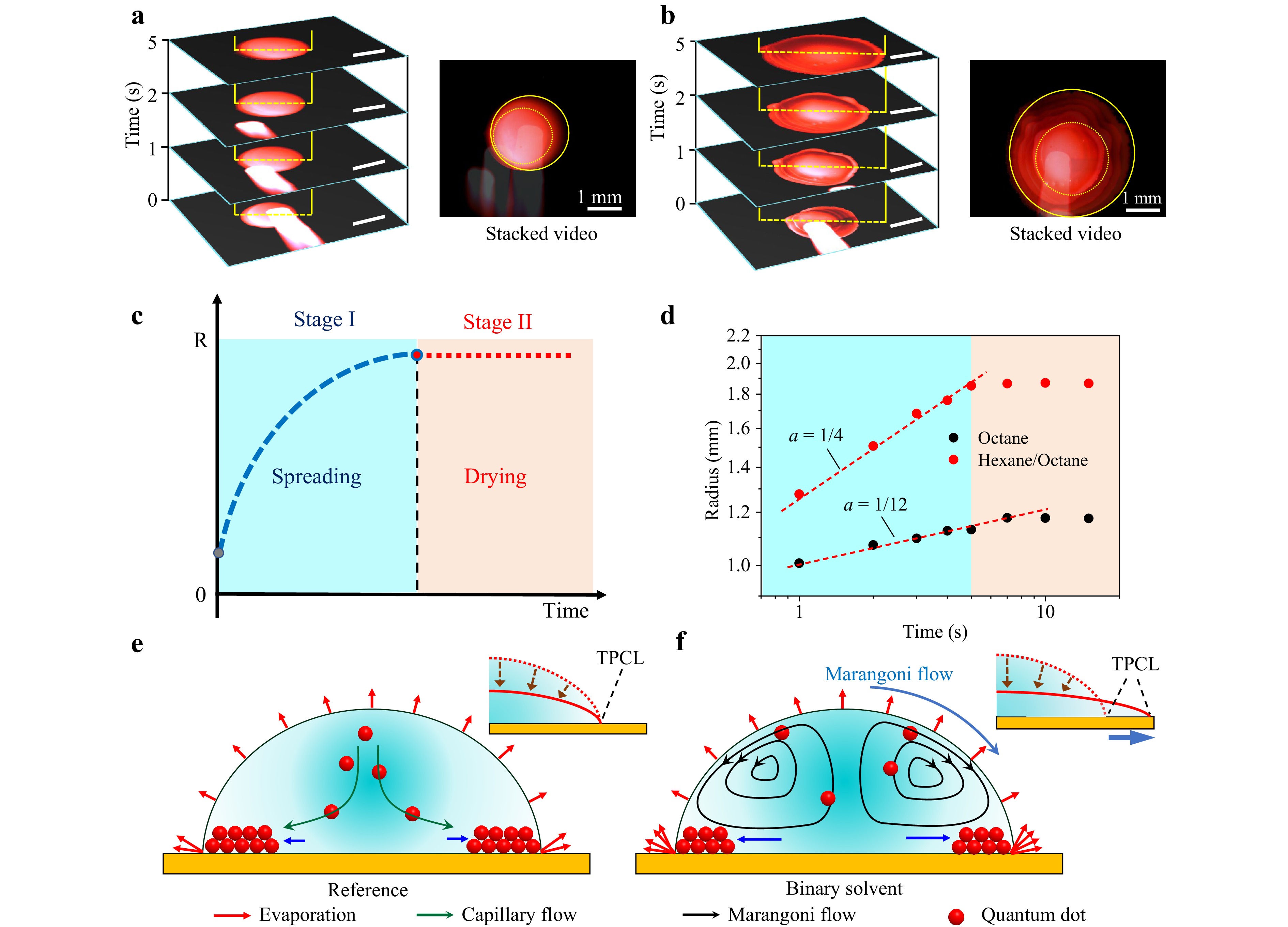
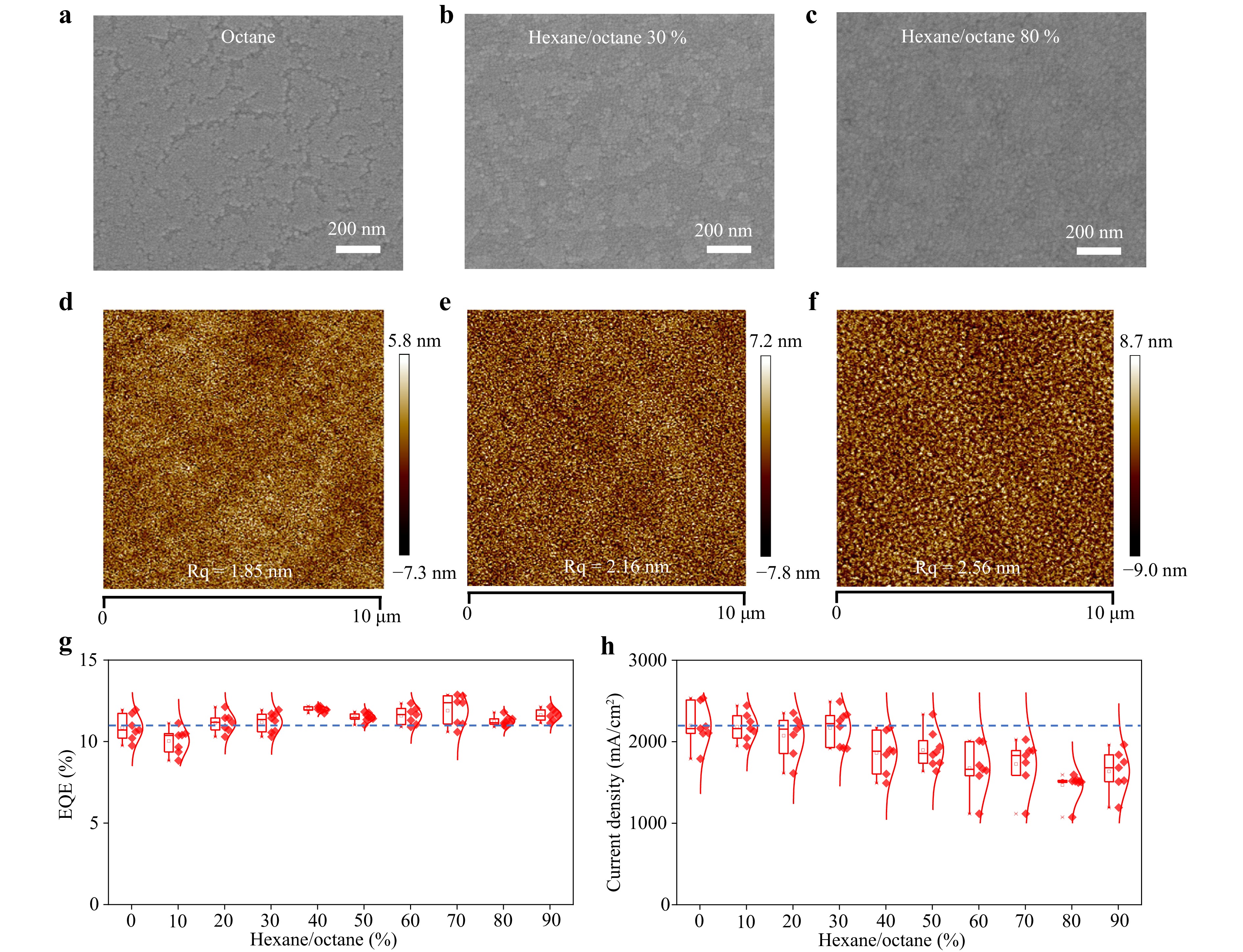
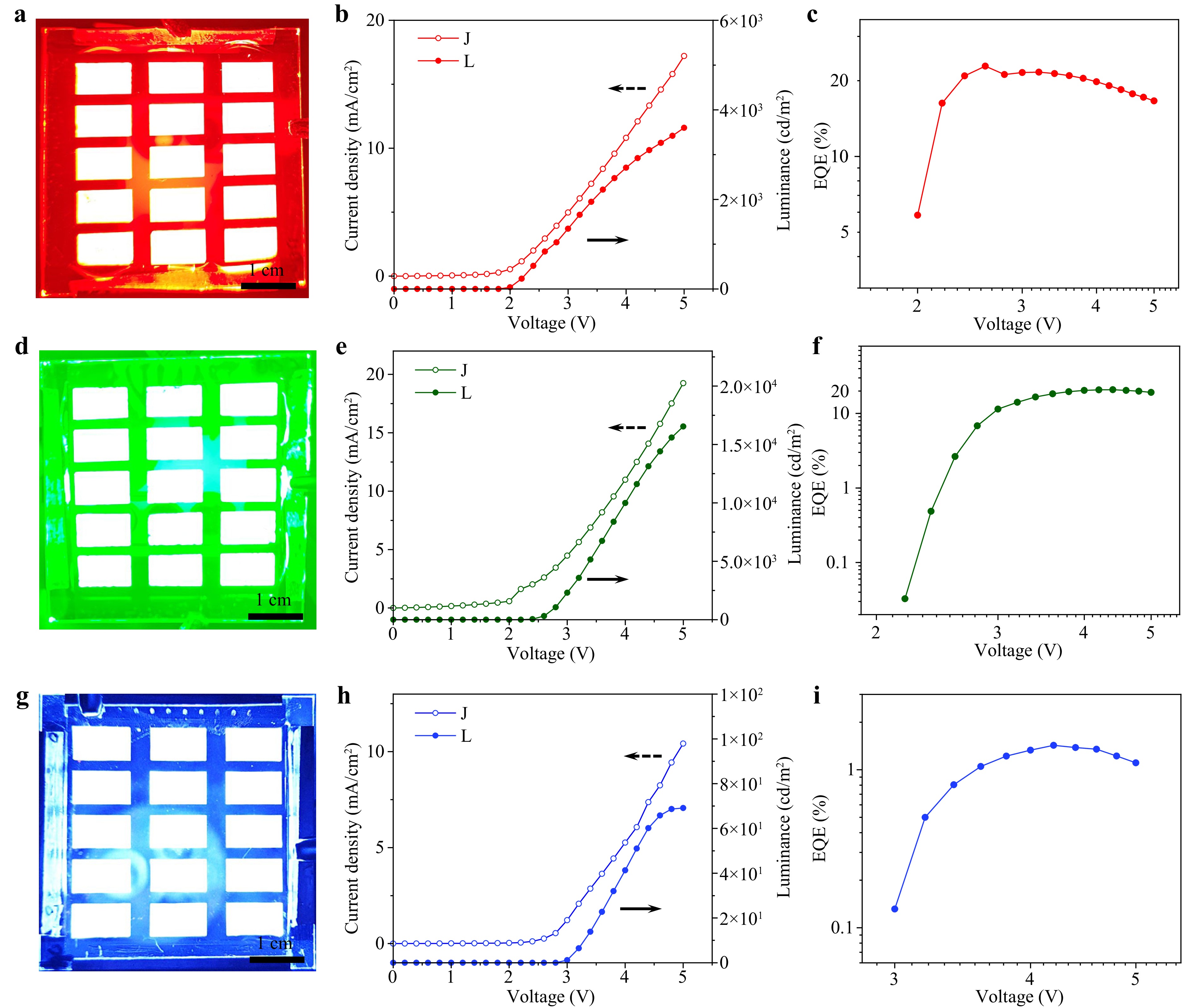
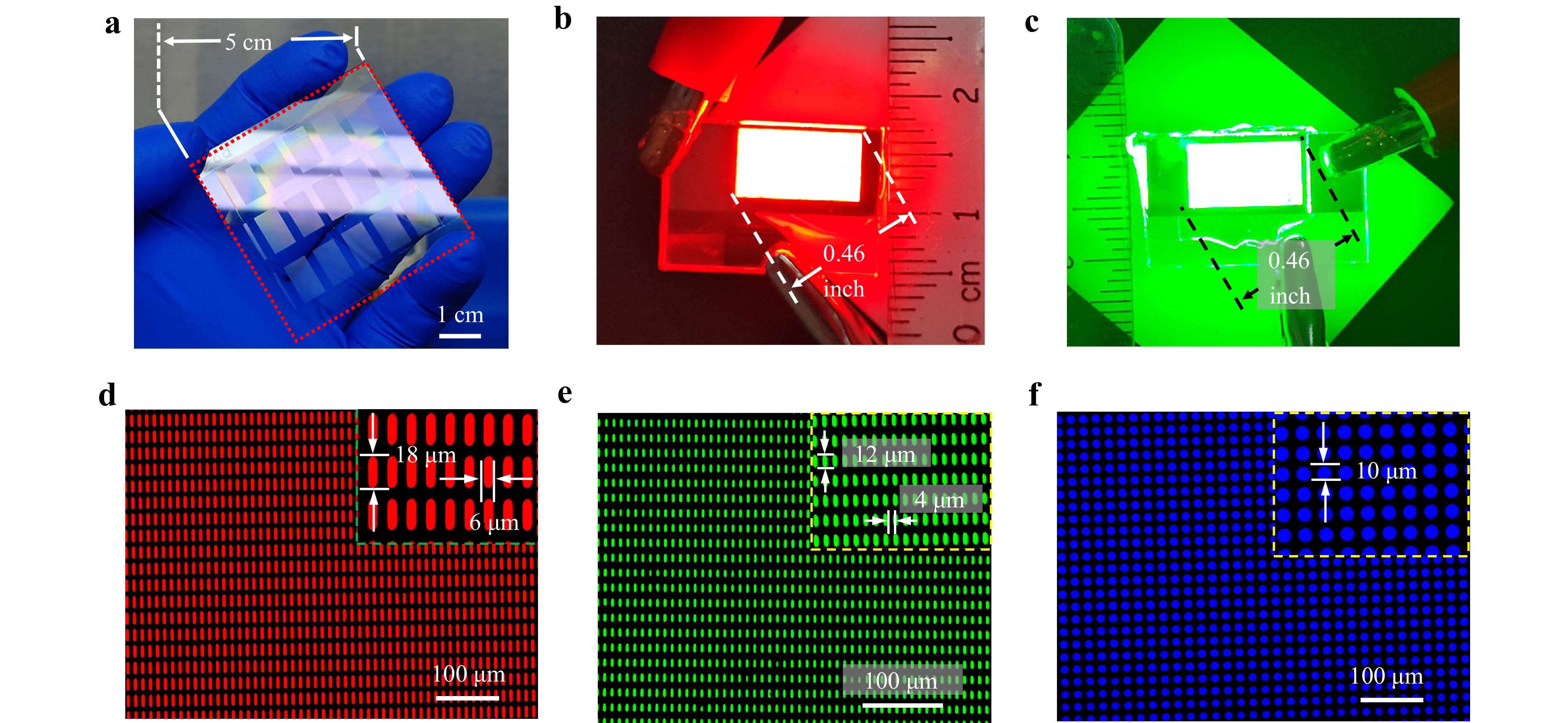
Micrometre-sized quantum-dot light-emitting diodes (Micro-QLEDs) have been successfully demonstrated as a promising technology for augmented reality (AR) microdisplay applications. To facilitate industrial applications, we developed a two-inch wafer-scale fabrication process for Micro-QLEDs, including the fabrication of a photolithography template, spin-coating fabrication of a QLED, and dicing of a 2-inch wafer into 0.46-inch Micro-QLED panels. Considering the challenge posed by the limited droplet spreading of quantum dots during spin-coating fabrication, we introduced a binary solvent of hexane and octane to achieve a wafer-scale spreading area. In situ high-speed microscopic observations revealed the critical role of Marangoni flow in determining the dynamics of a three-phase contact line. We further designed a 2-inch wafer-scale fabrication process for Micro-QLEDs with an active emitting area of 1,600 mm2, which provides fifteen microdisplay panels with a 0.46-inch Micro-QLED per wafer, achieving a resolution of 2,510 pixels per inch (a pixel size range of 4–50 μm). In addition, the red, green, and blue Micro-QLED wafers had high external quantum efficiencies of 22.8%, 20.8%, and 1.4%, respectively. The 2-inch wafer-scale fabrication process for Micro-QLEDs provides a feasible method for the industrialisation of Micro-QLED technology.
Published. 2026, 7(3)
: 971-982
doi: 10.37188/lam.2026.103
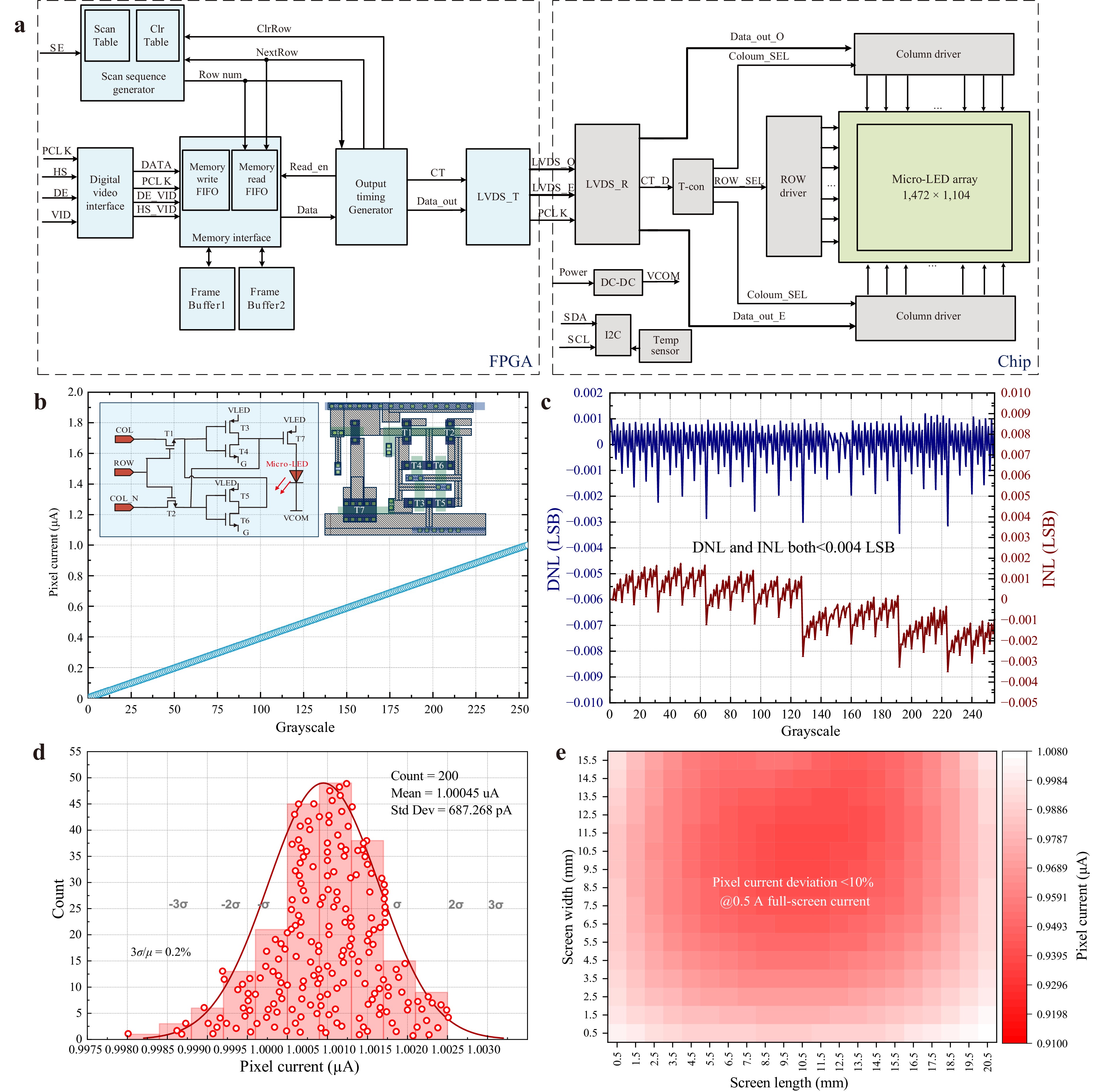
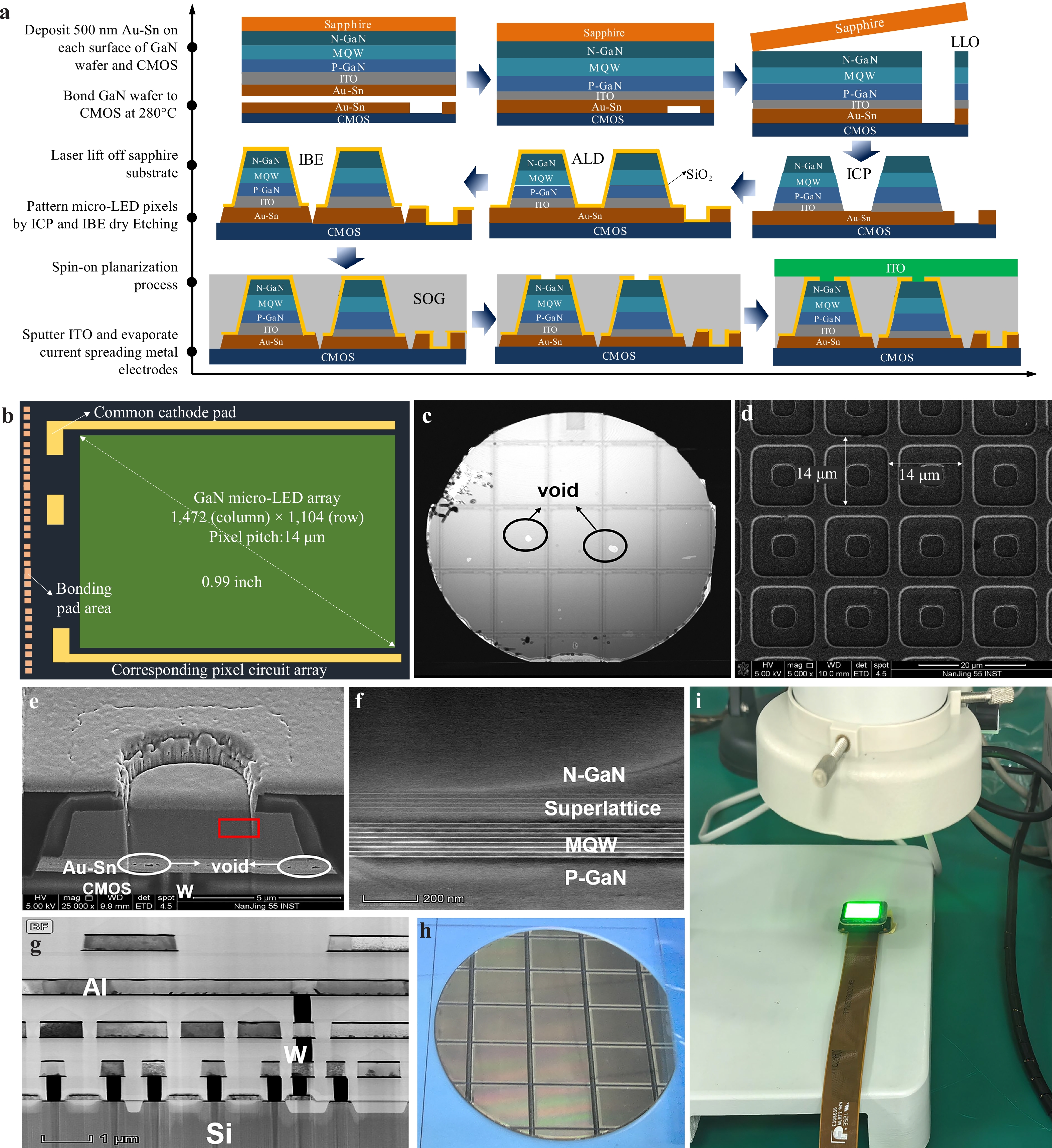
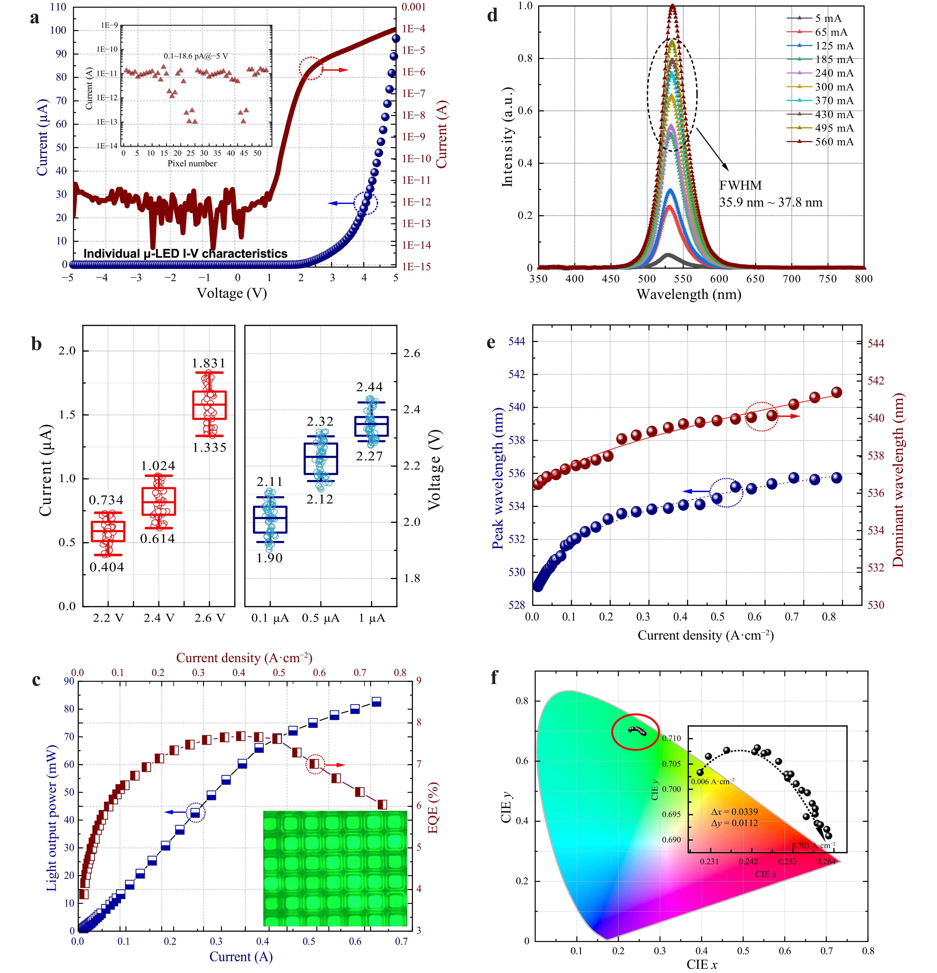
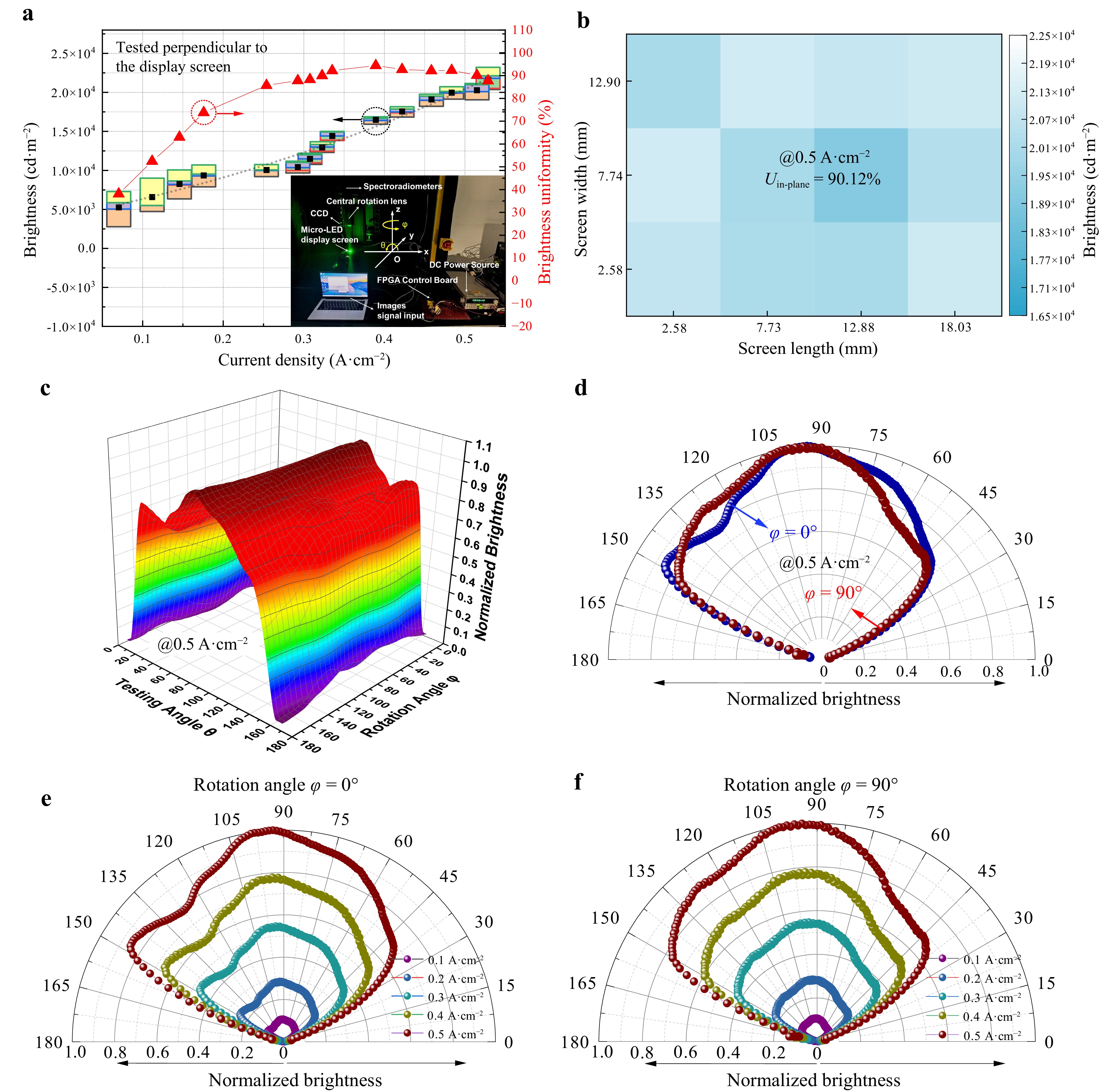
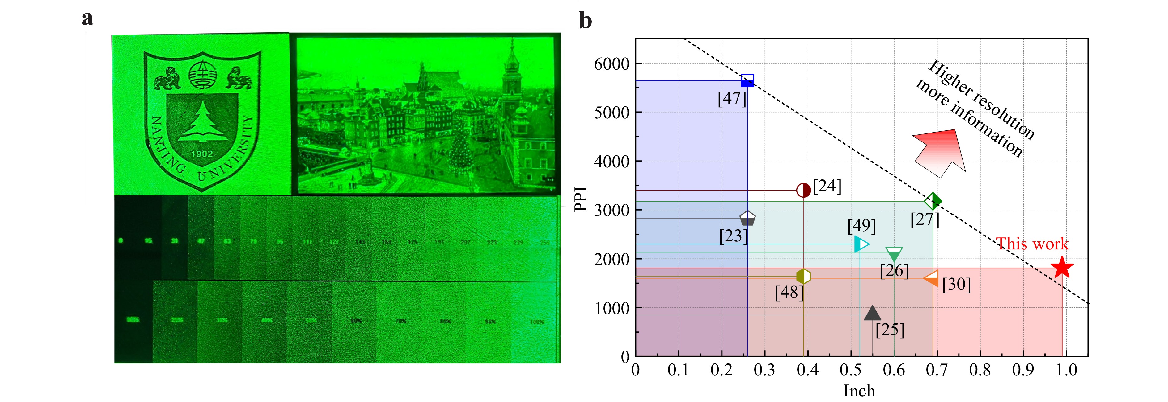
Micro-light-emitting diode (micro-LED) displays are prime candidates for near-eye displays, where increasing the panel diagonal at a fixed pixel density is essential to expand the field of view. However, scaling the active area while maintaining luminance homogeneity presents a challenge, primarily due to the pixel-to-pixel current variation in CMOS driven and process-induced non-uniformities in LED arrays. Here we address this trade-off by combining per-pixel current regulation with an optimized fabrication flow in a heterogeneous integration strategy that couples green GaN-based micro-LED with a custom Si CMOS backplane via wafer bonding. The resulting 0.99-inch prototype (1,472 × 1,104 pixels, 14 µm pitch, 1,814 PPI) exhibits >90% brightness uniformity across the active area, peak luminance exceeding 20,000 cd·m−2, a wide viewing angle (>120°), and excellent electrical consistency. These results demonstrate that our heterogeneous integration approach can chart a path toward larger, uniform, and power-efficient micro-displays.
Published. 2026, 7(3)
: 983-1023
doi: 10.37188/lam.2026.104
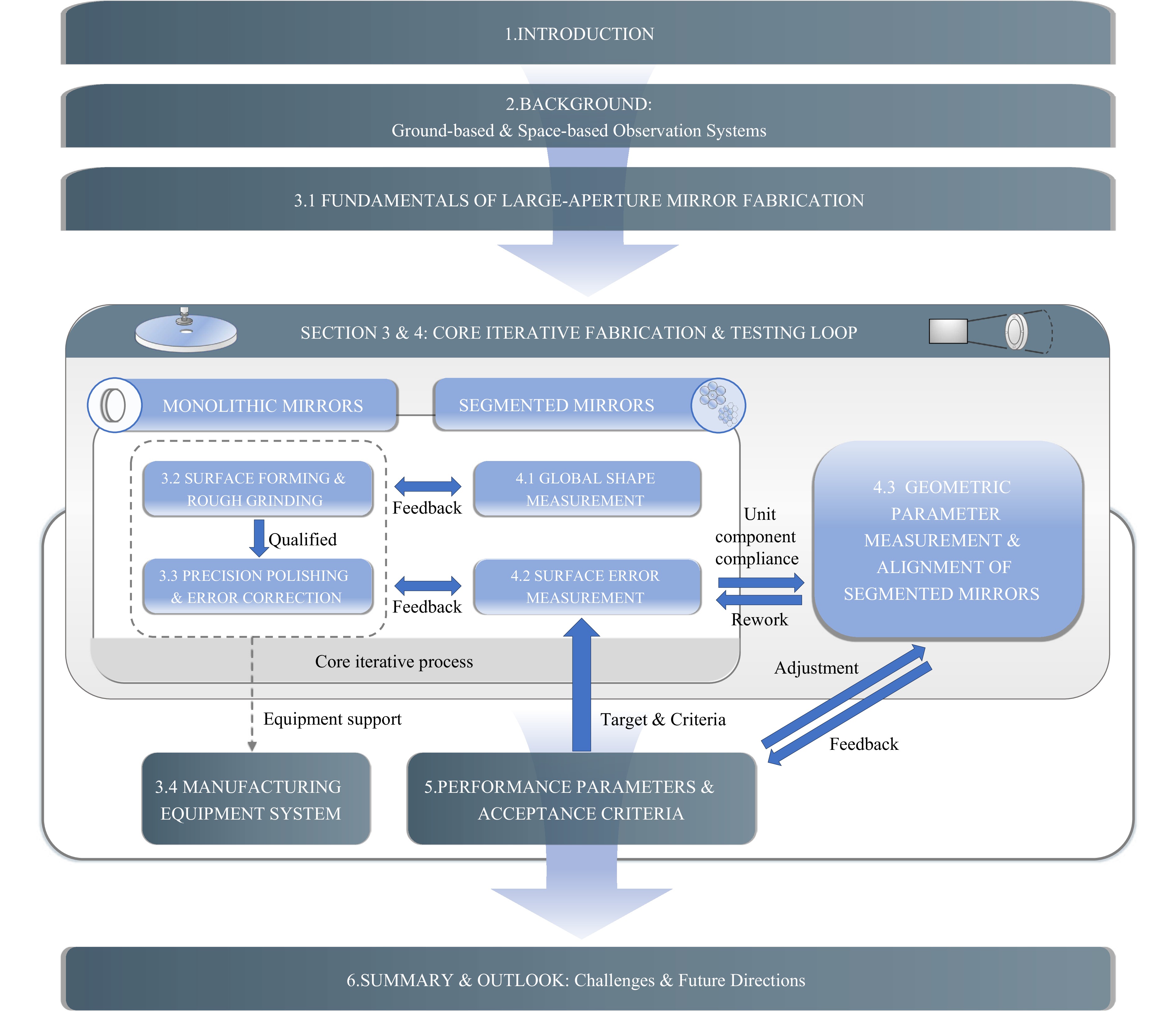
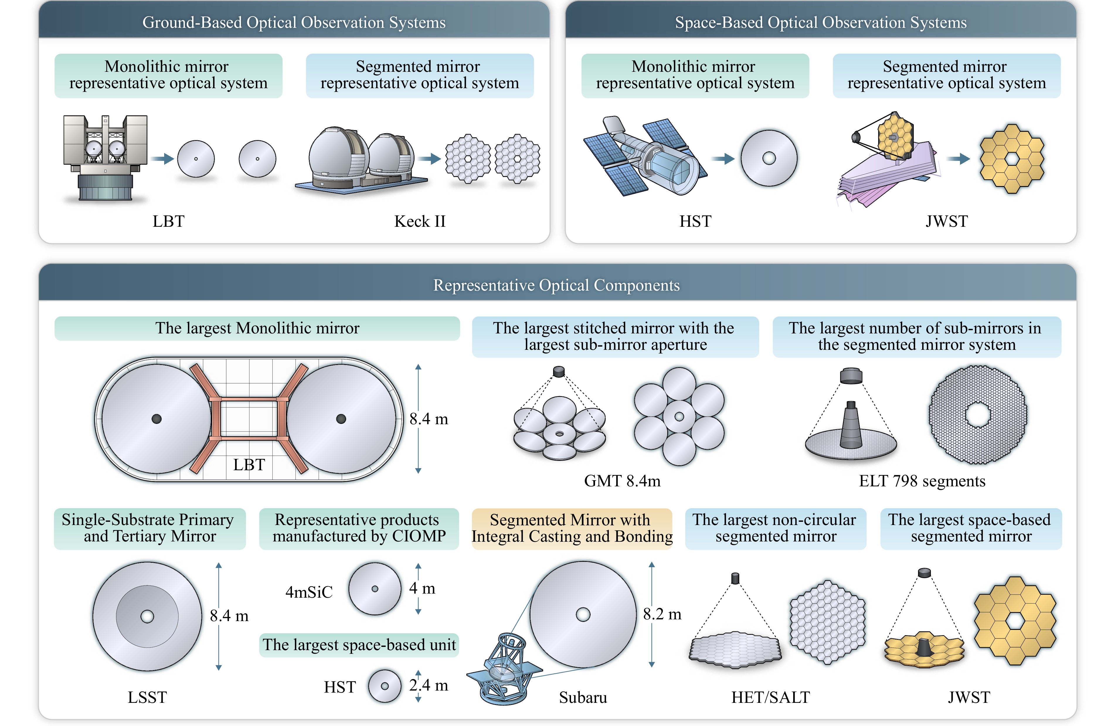
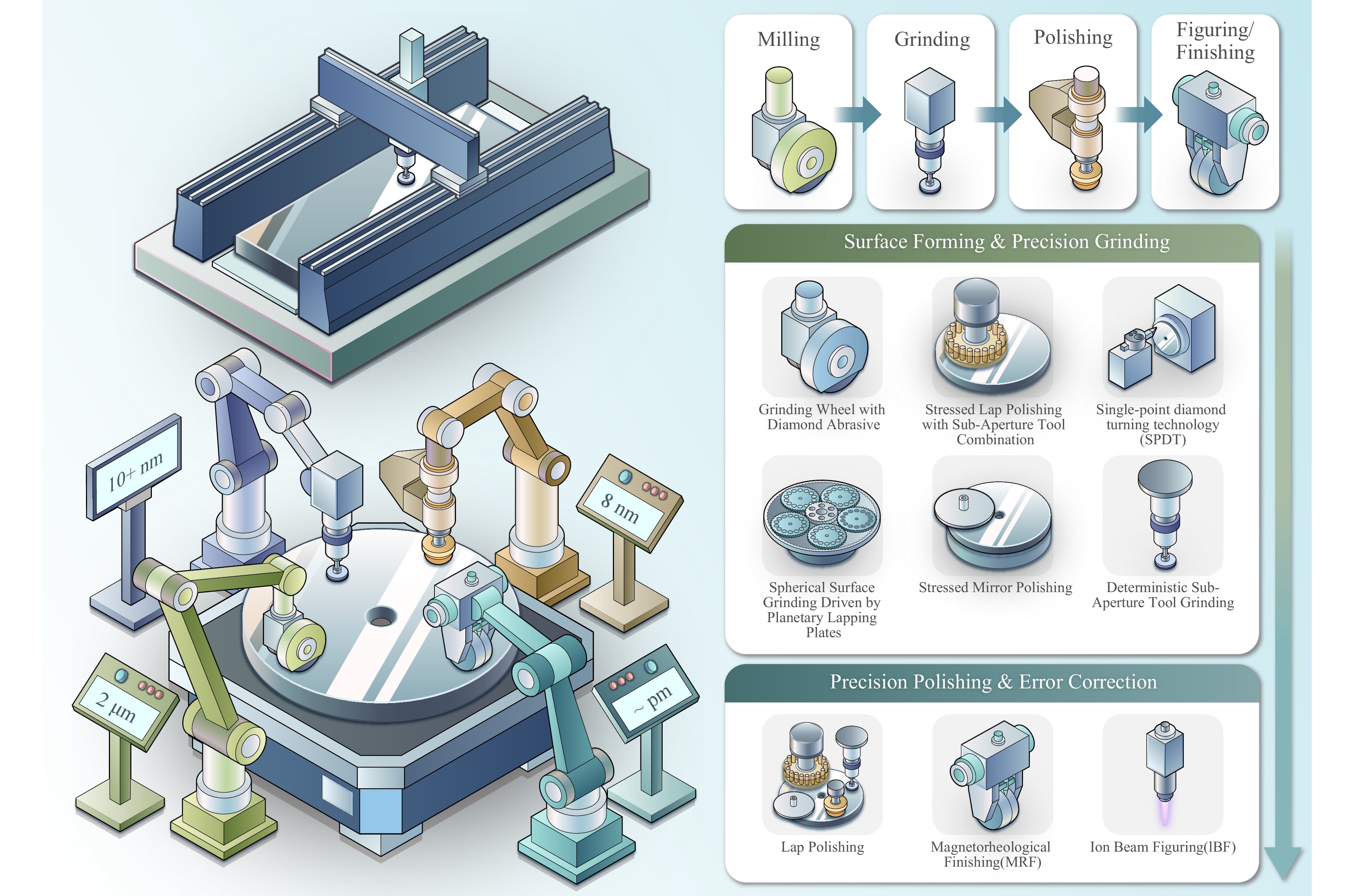
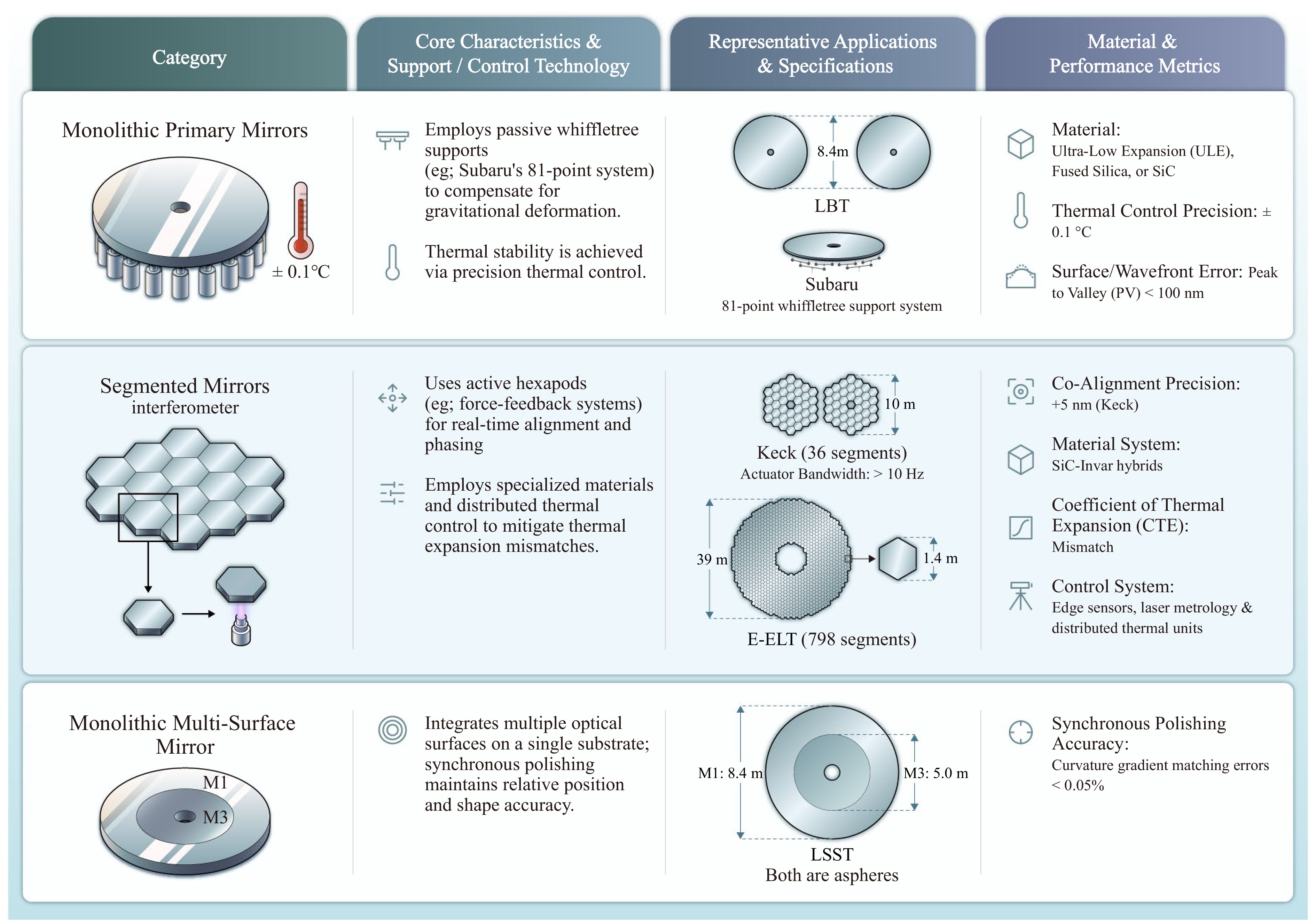
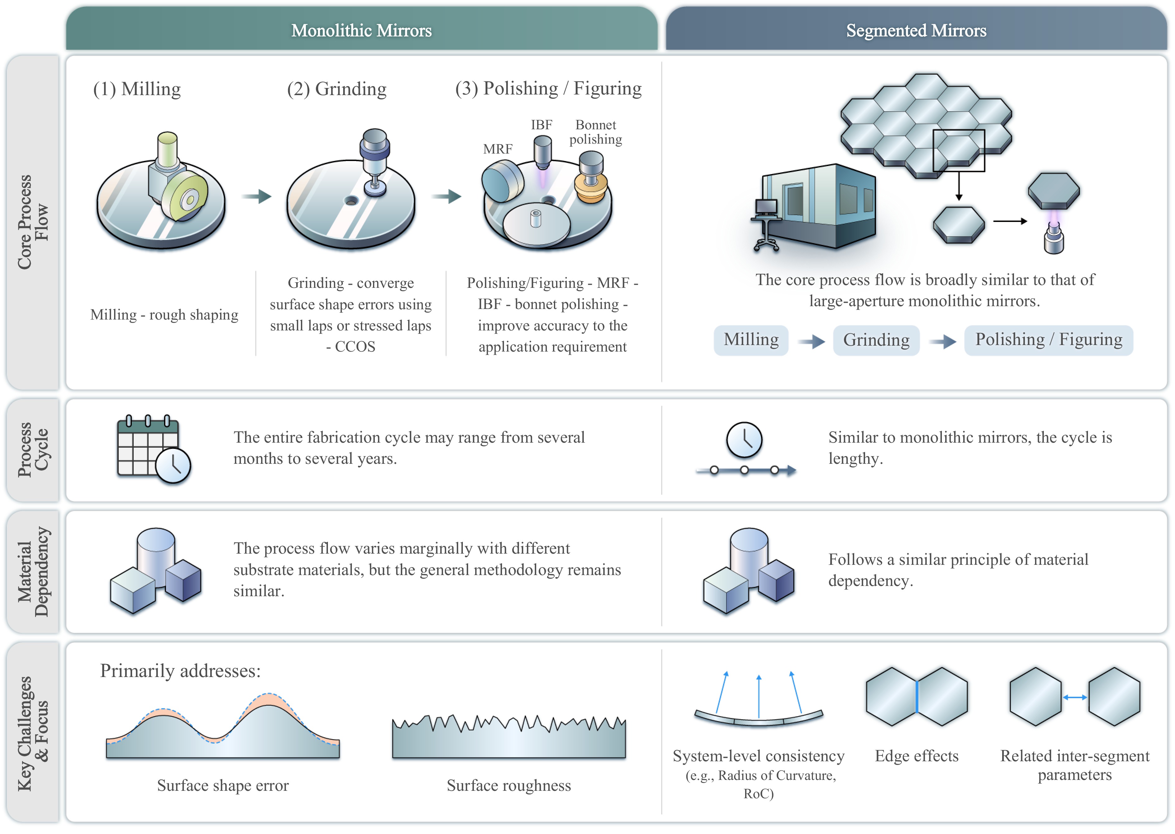
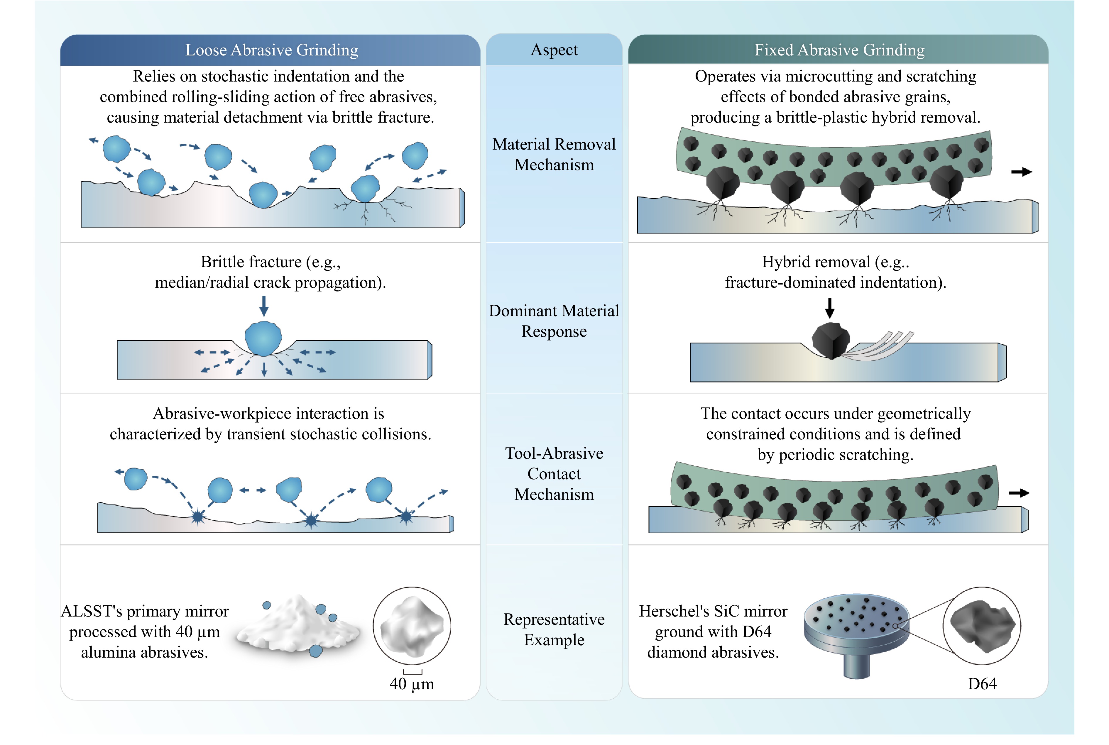
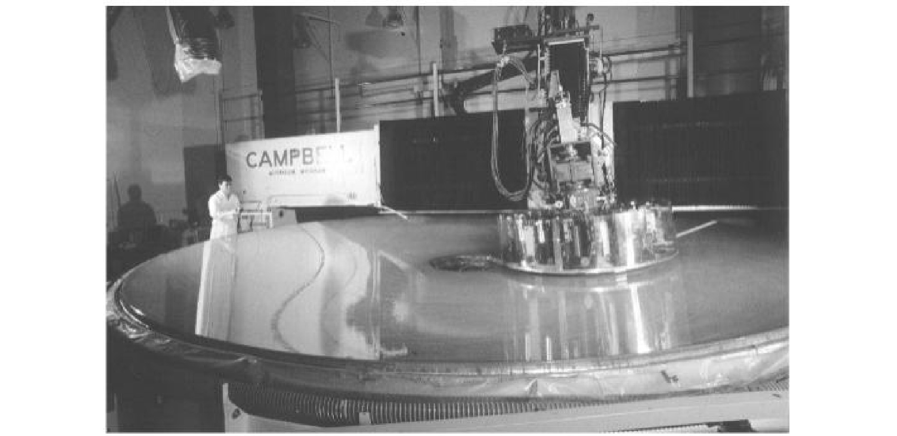
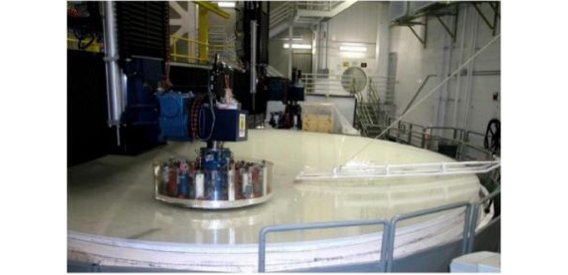
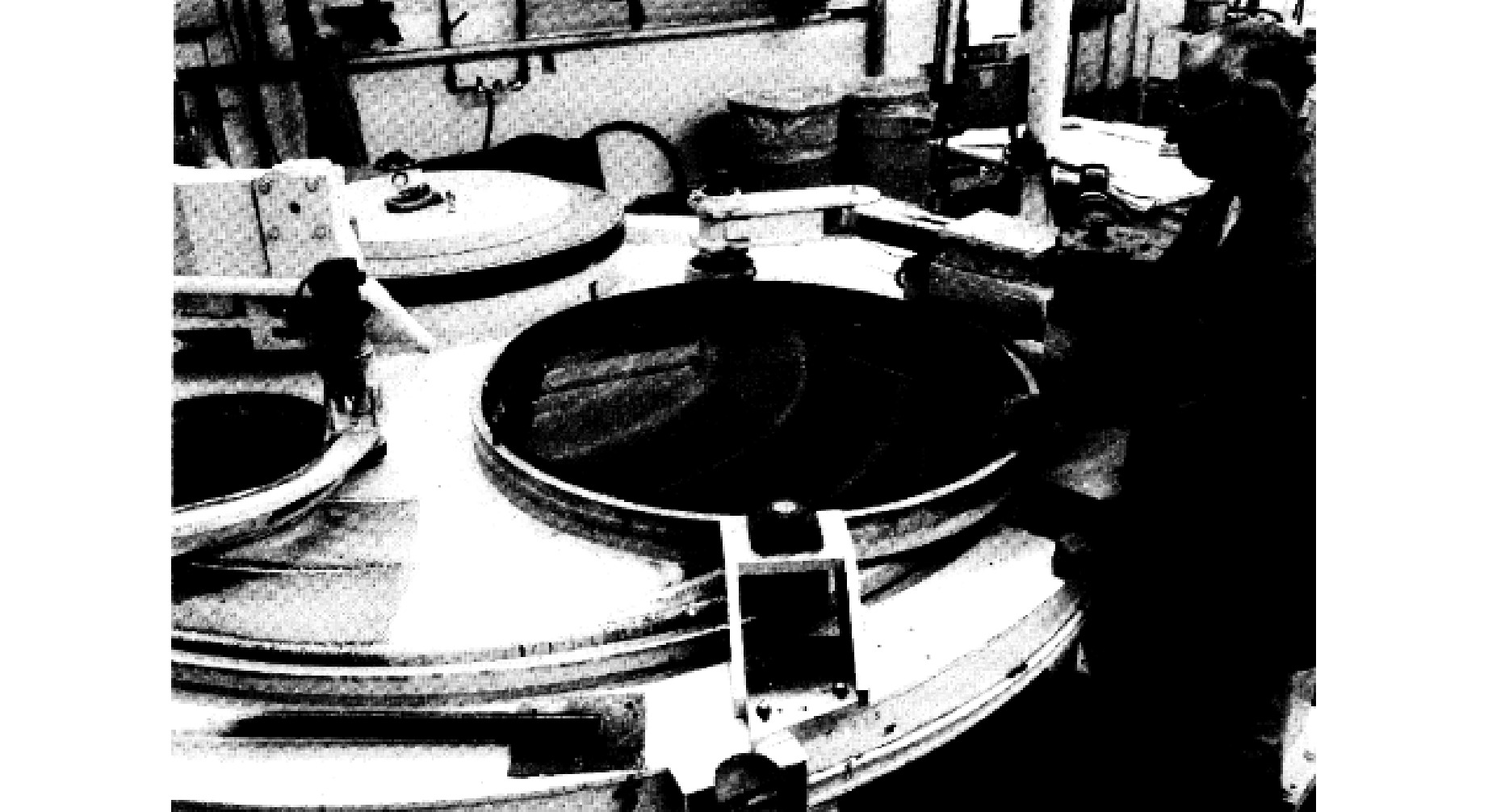
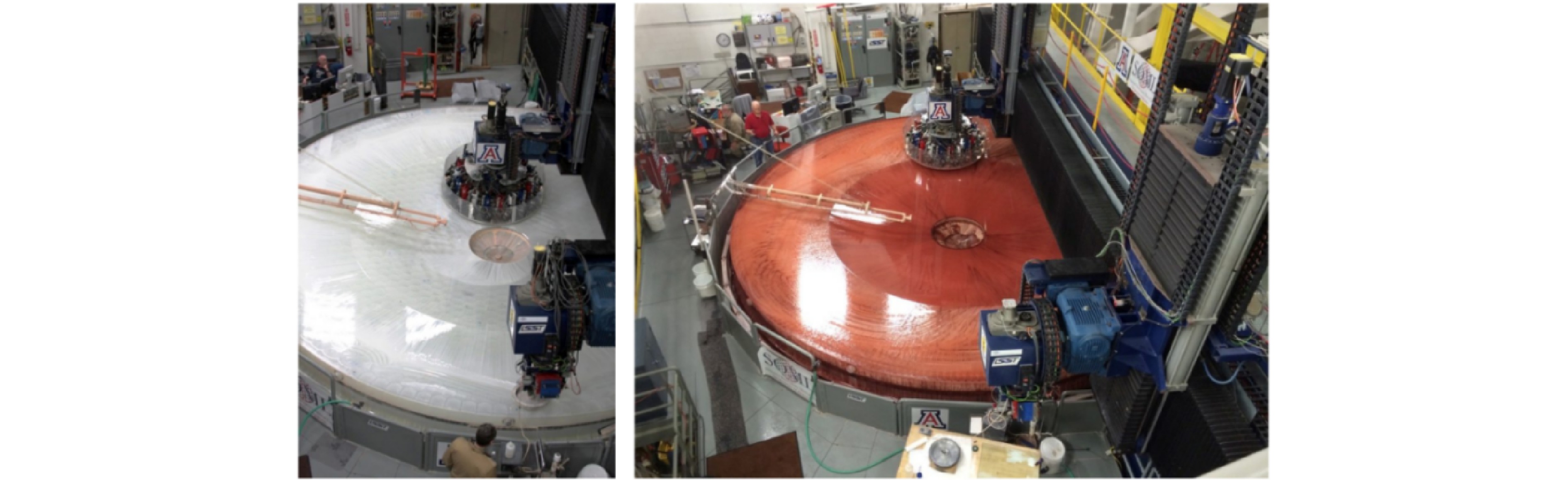
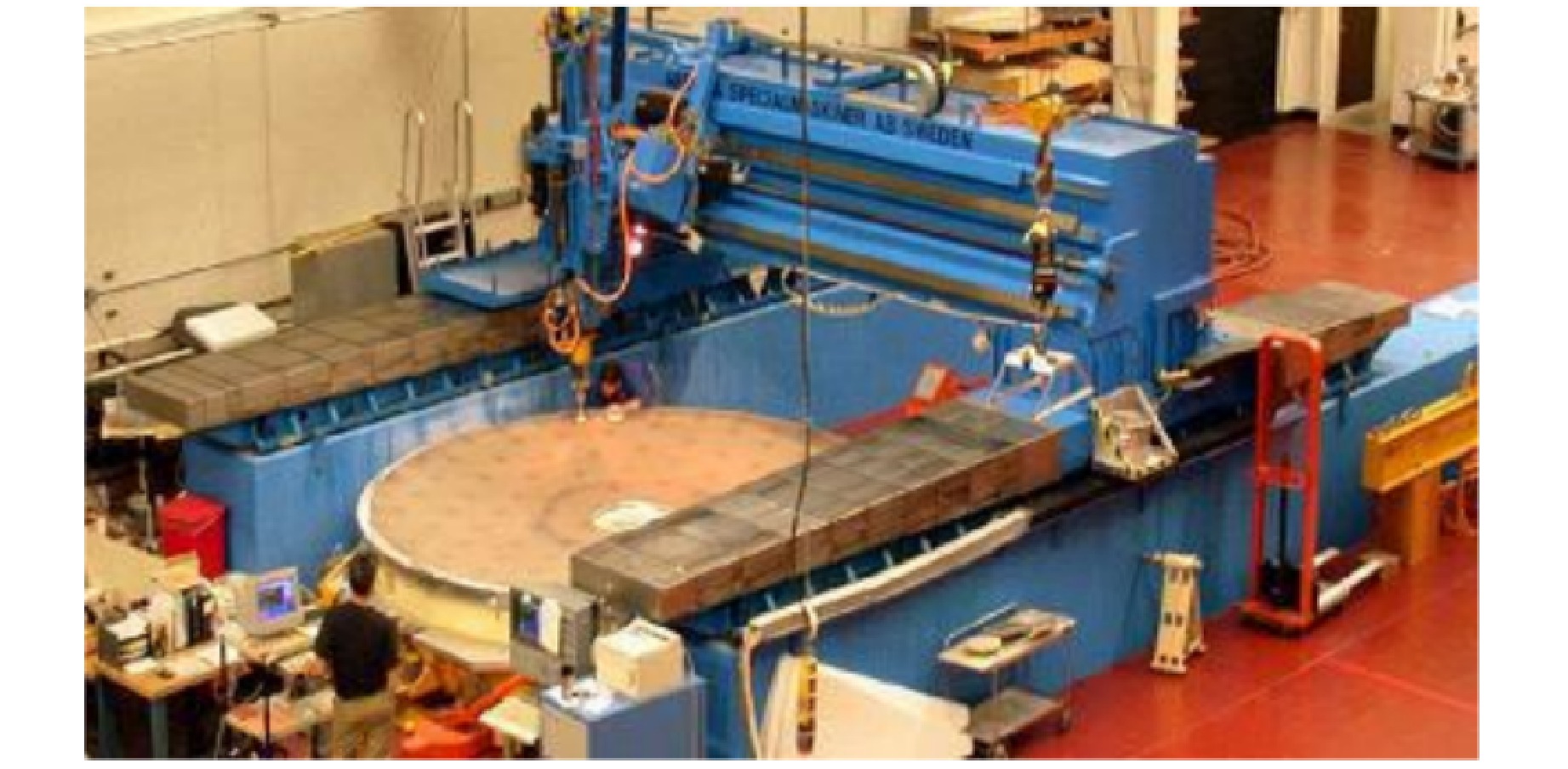
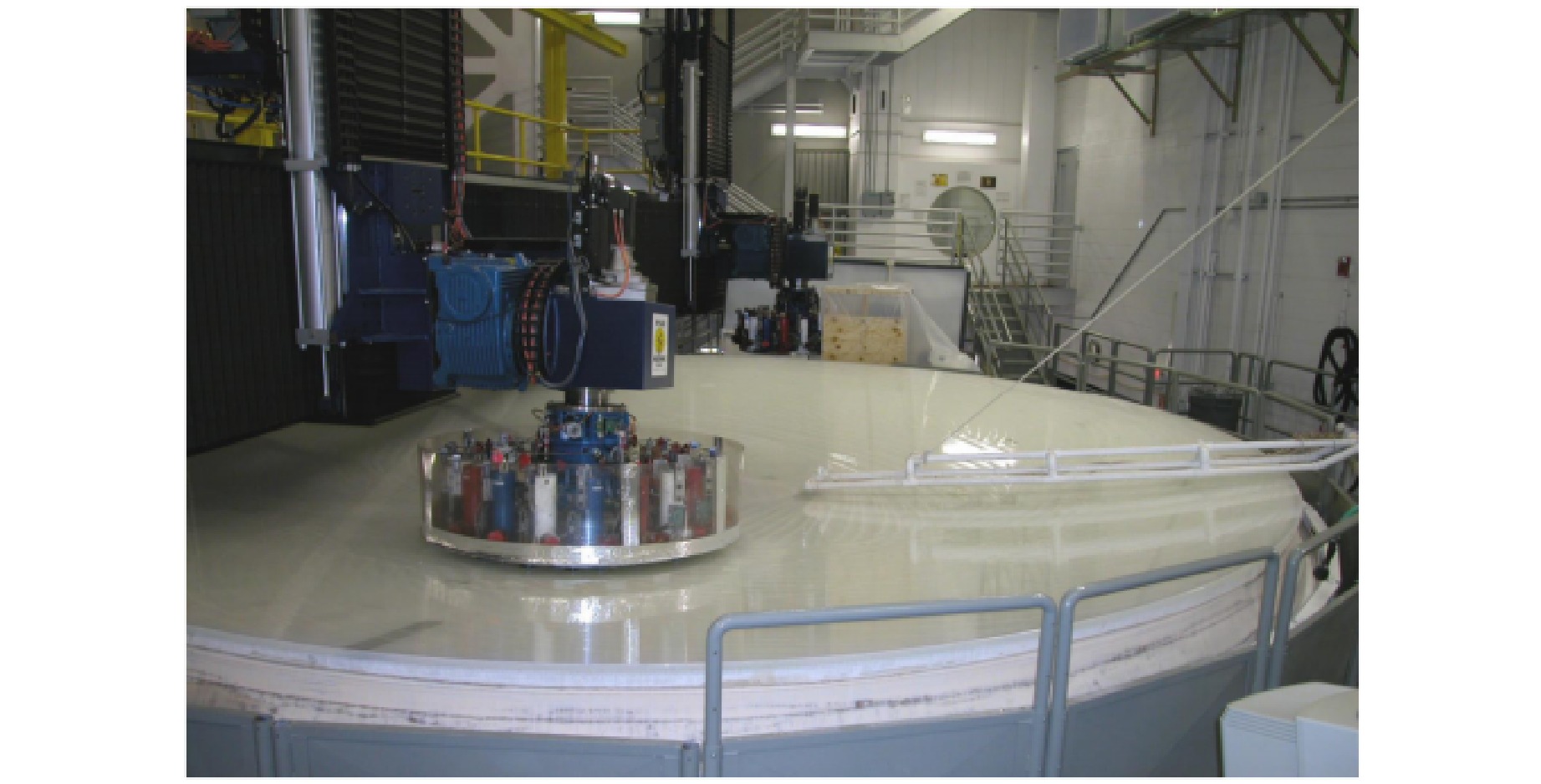
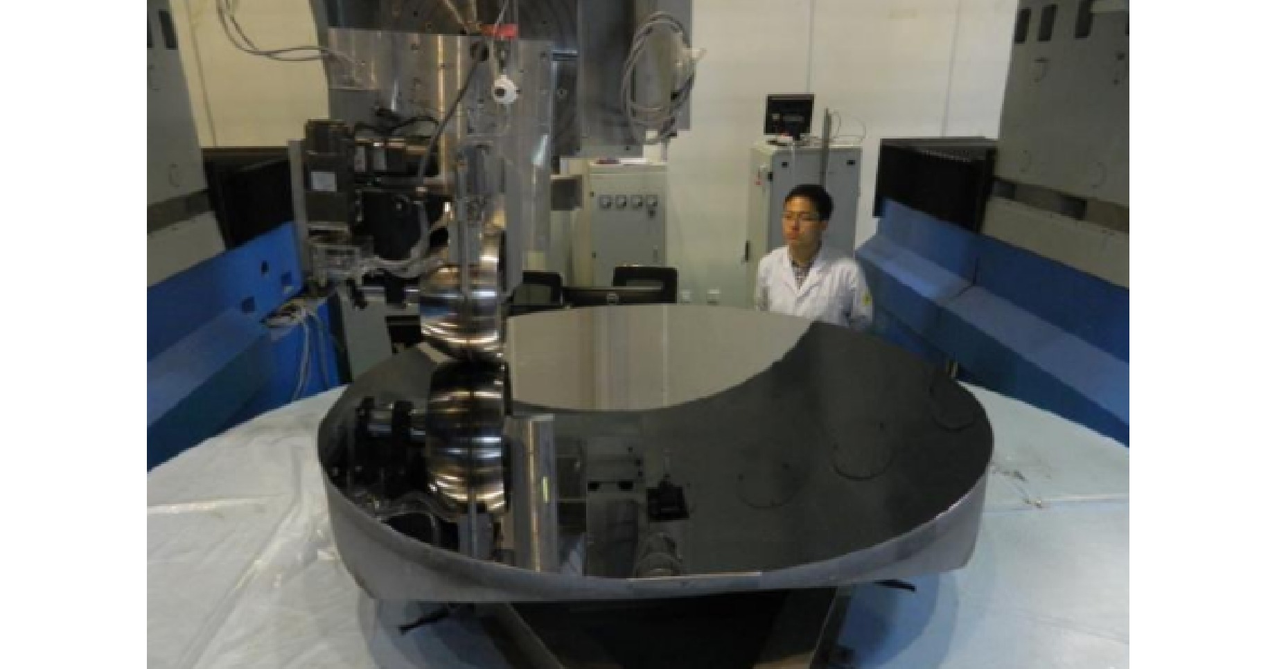
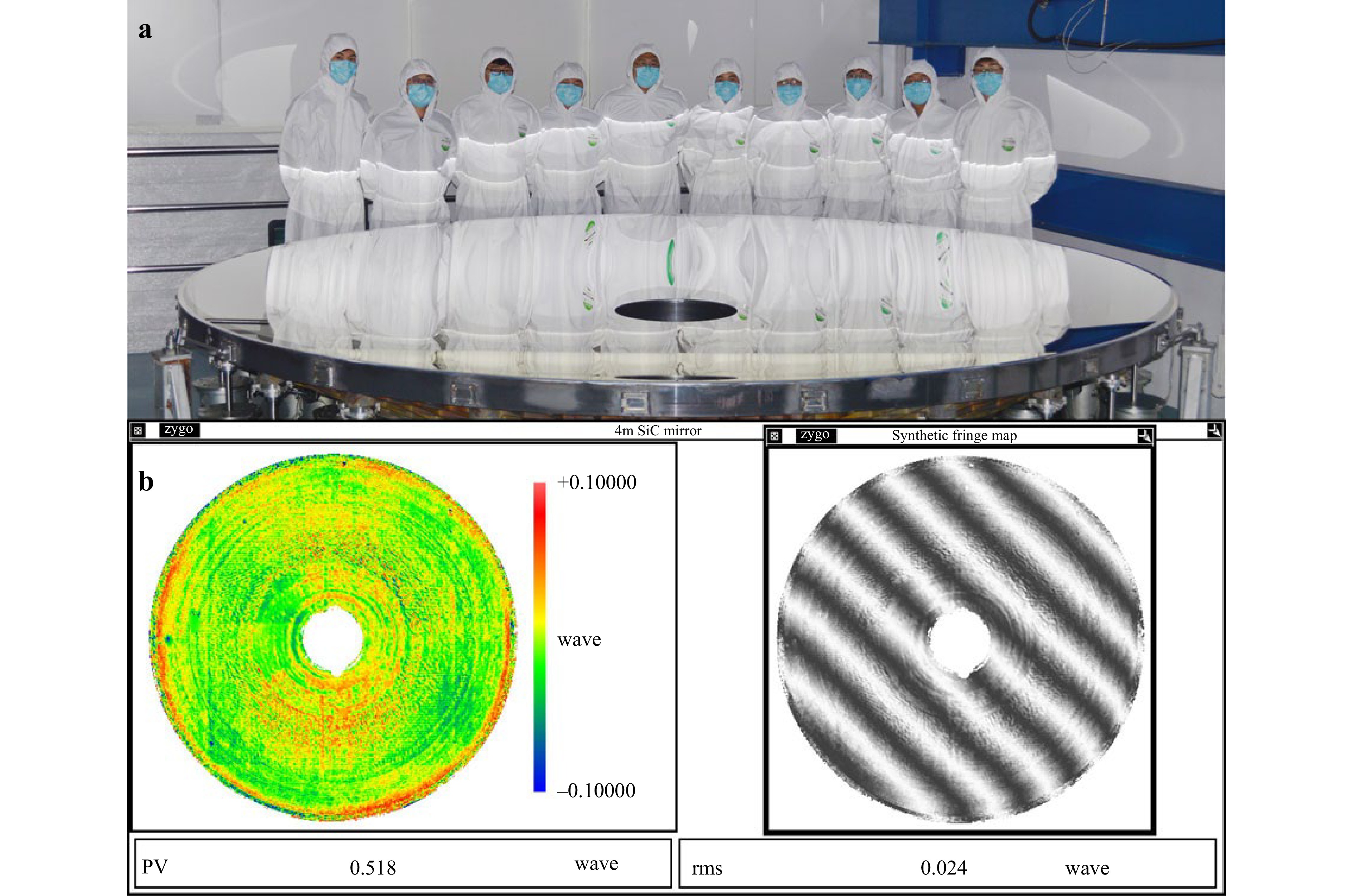
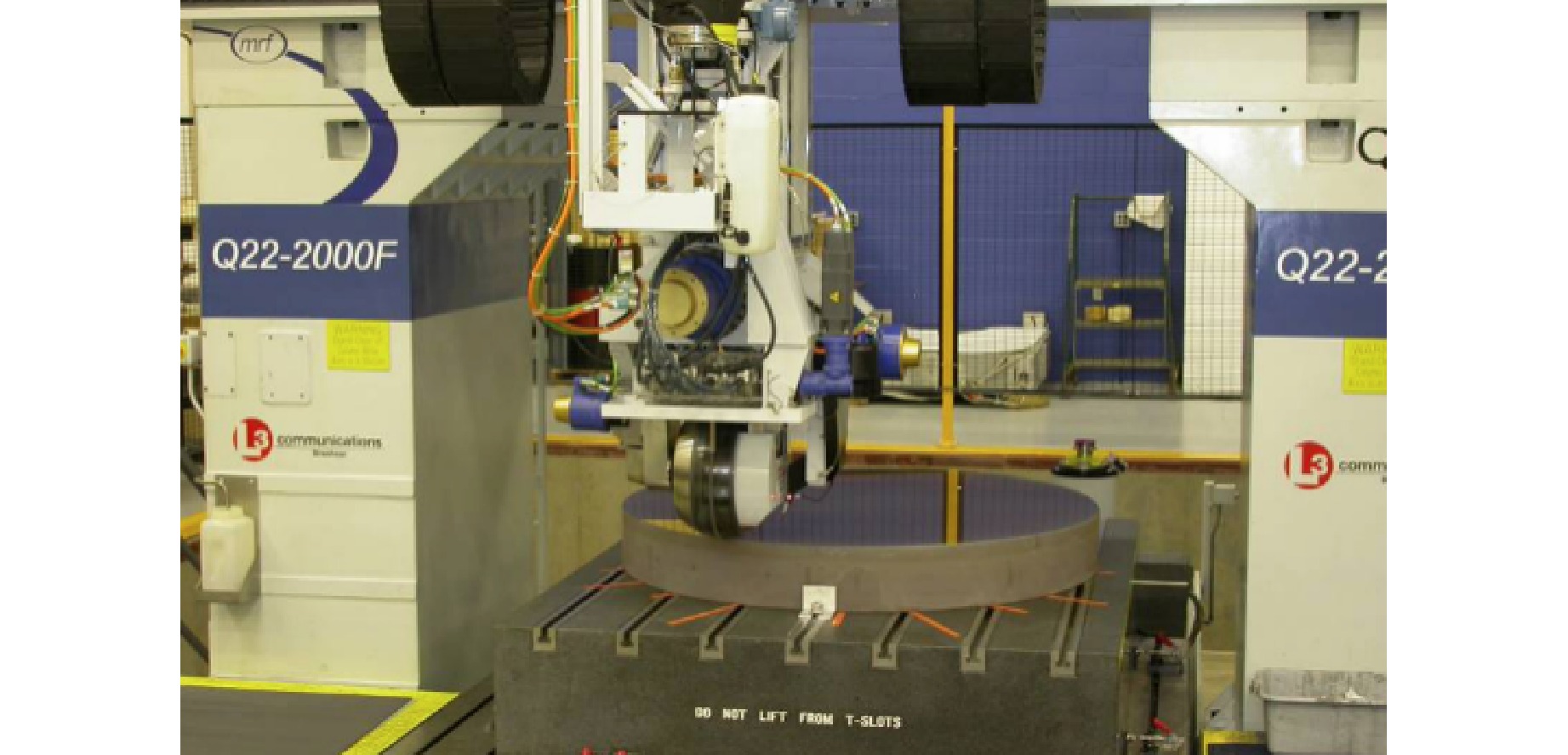
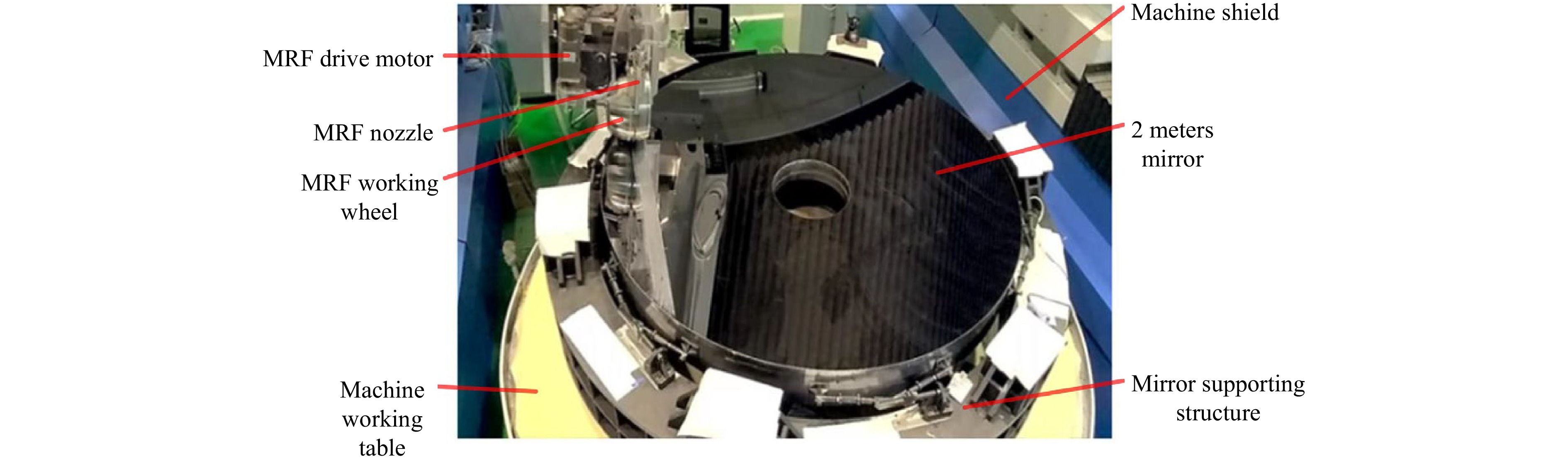
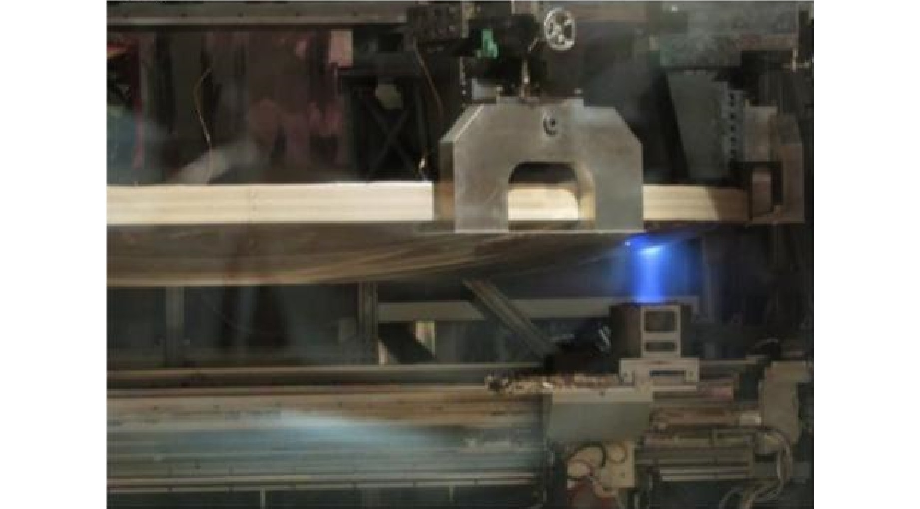
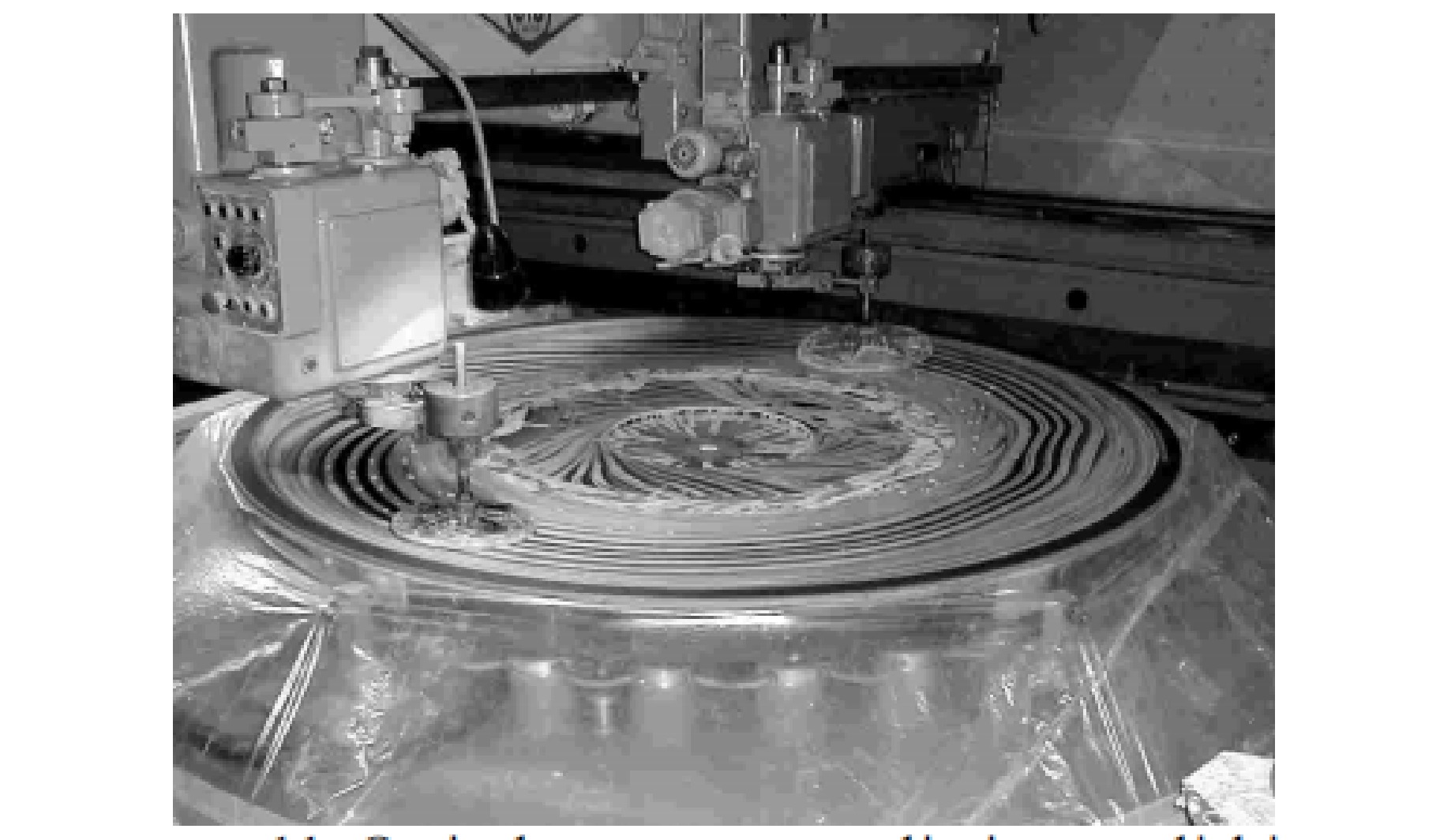
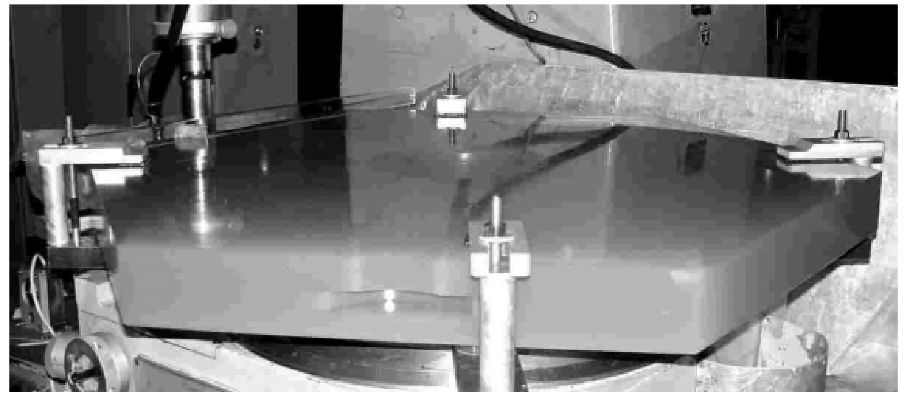
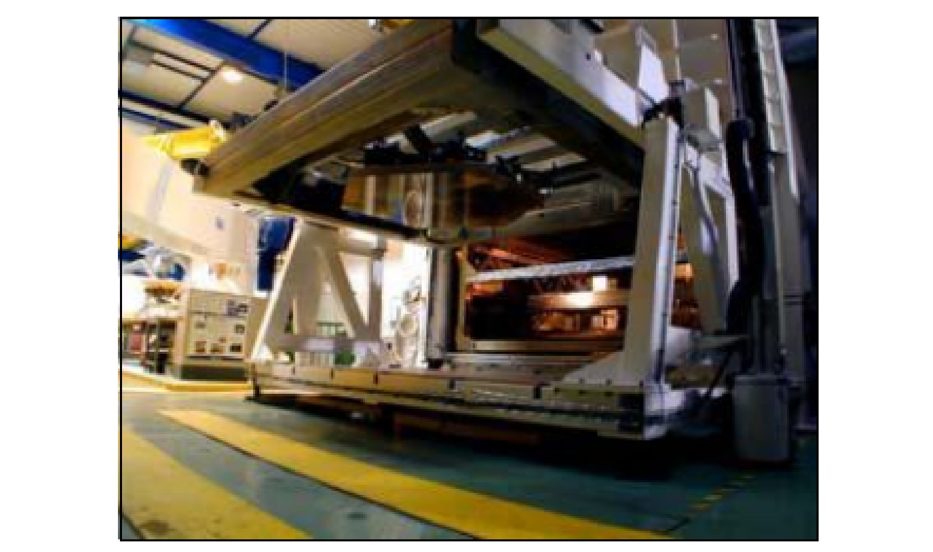
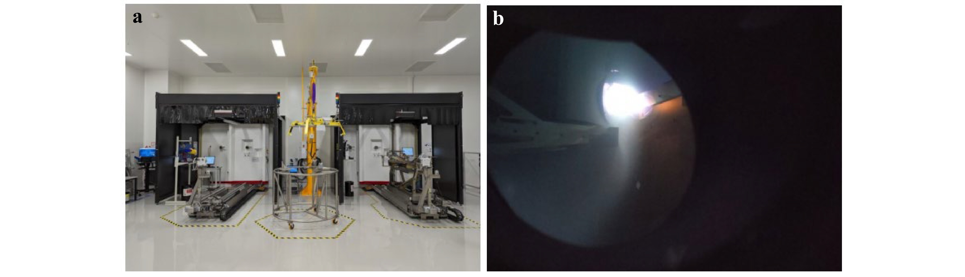
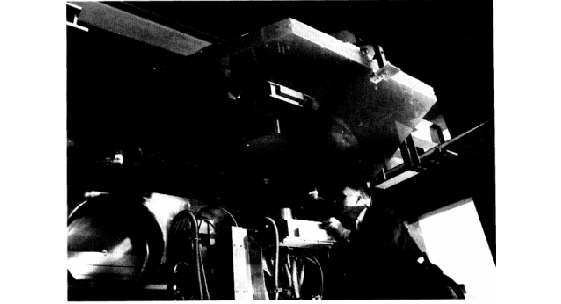
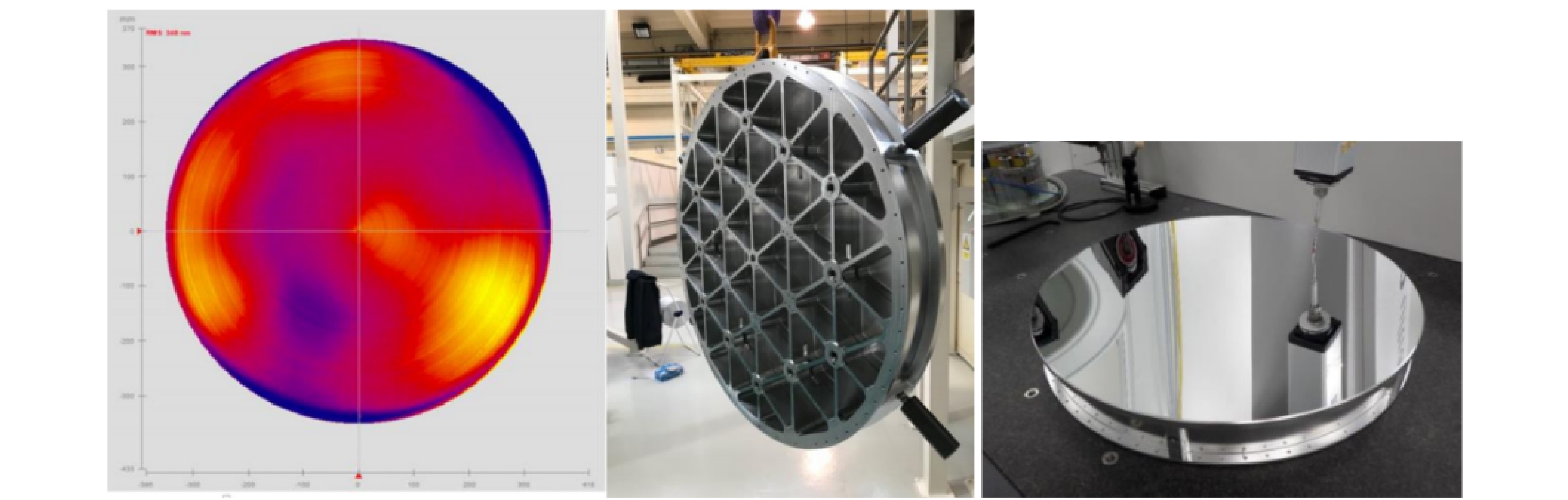
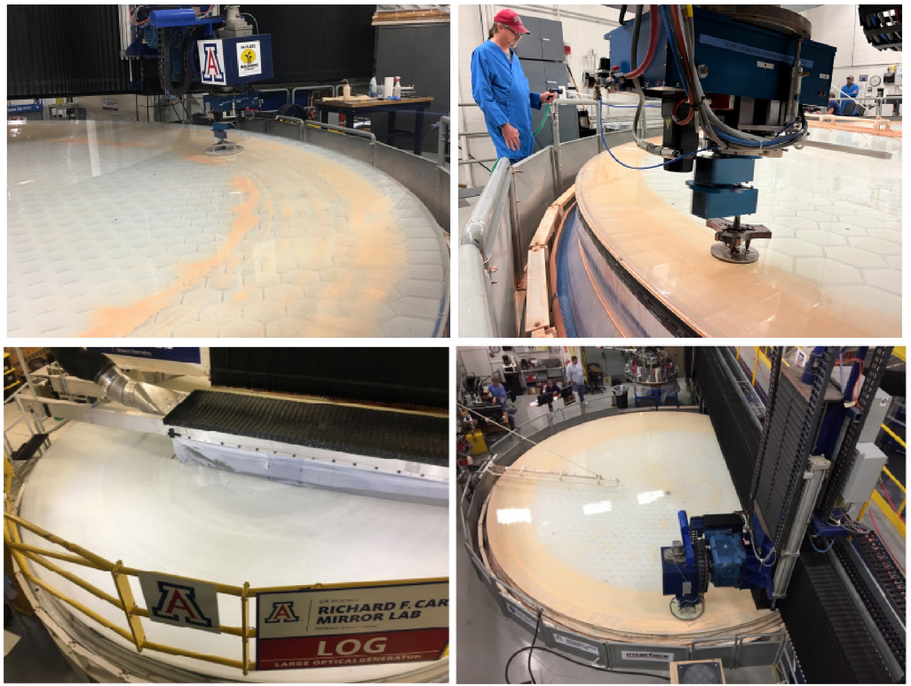
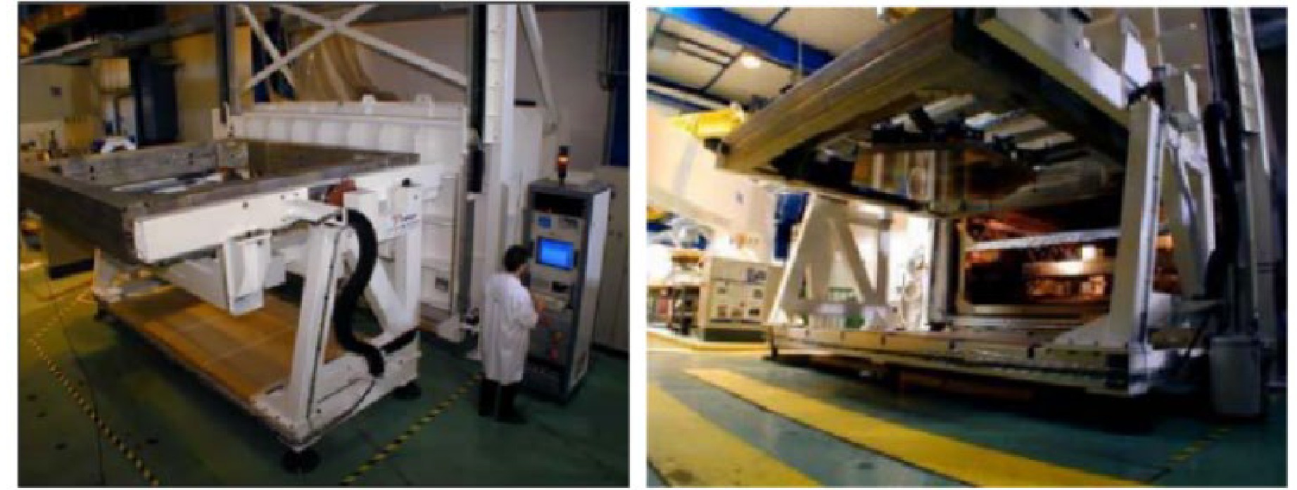
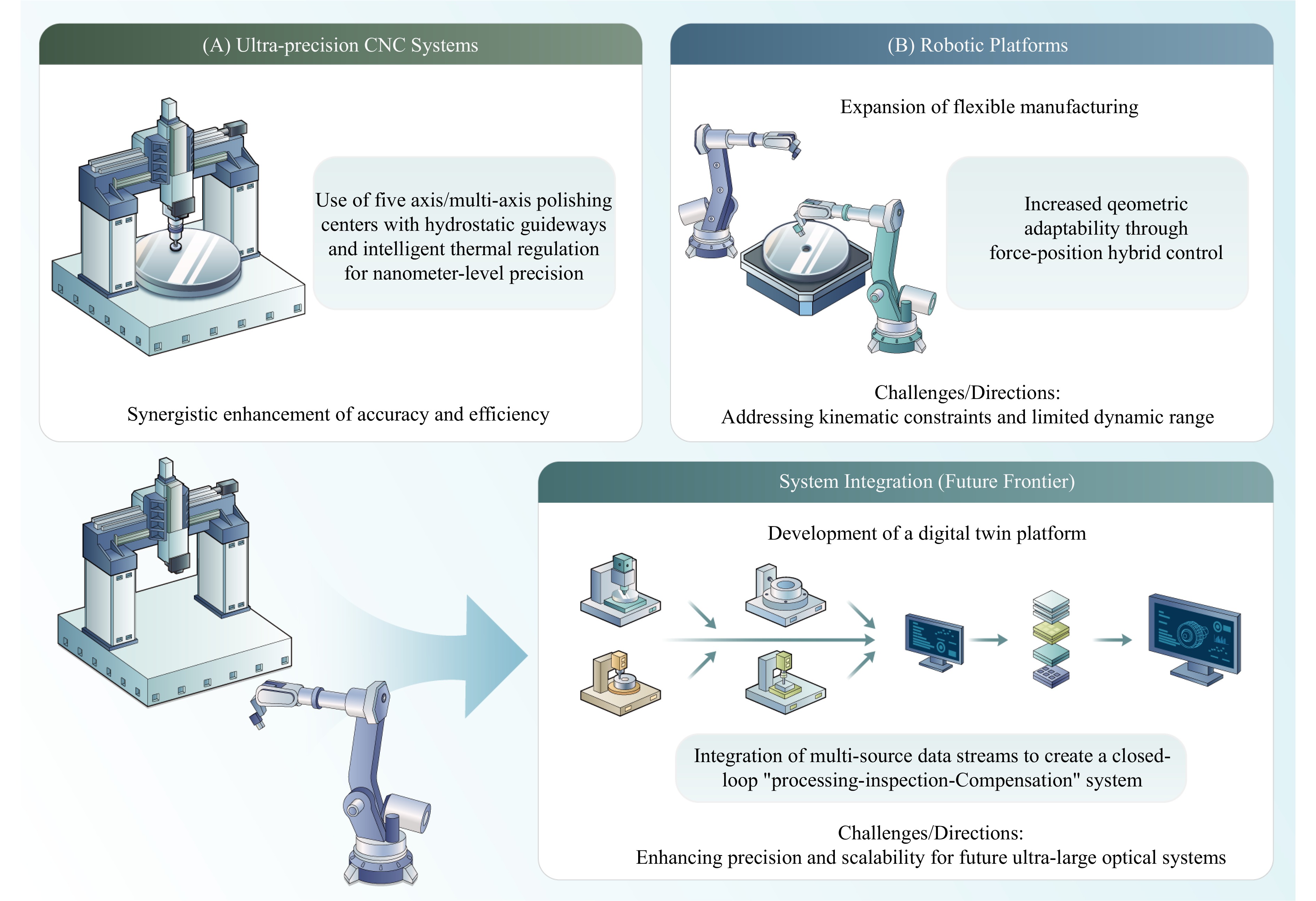
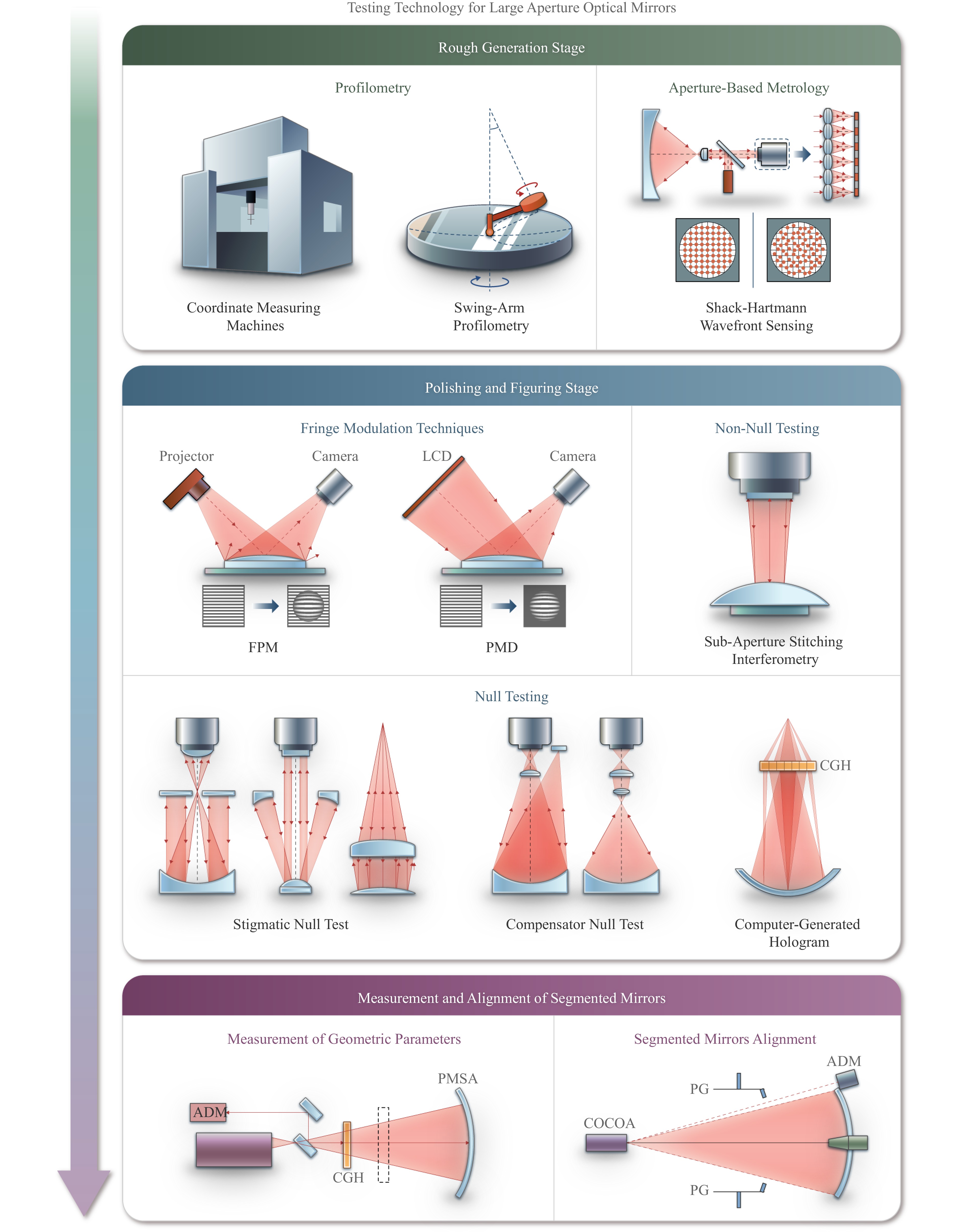
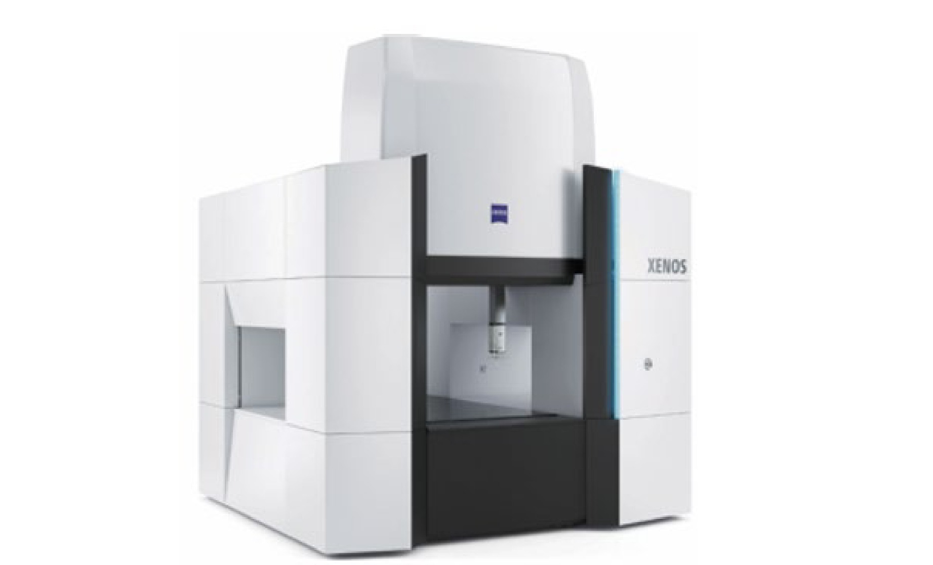
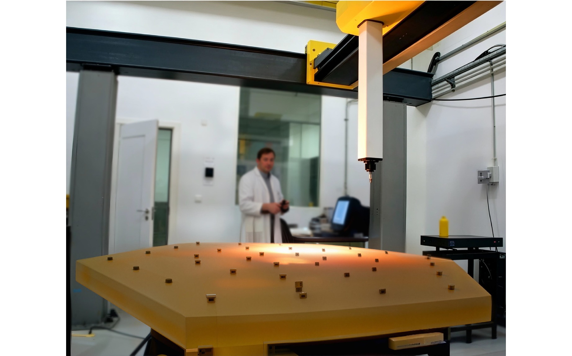
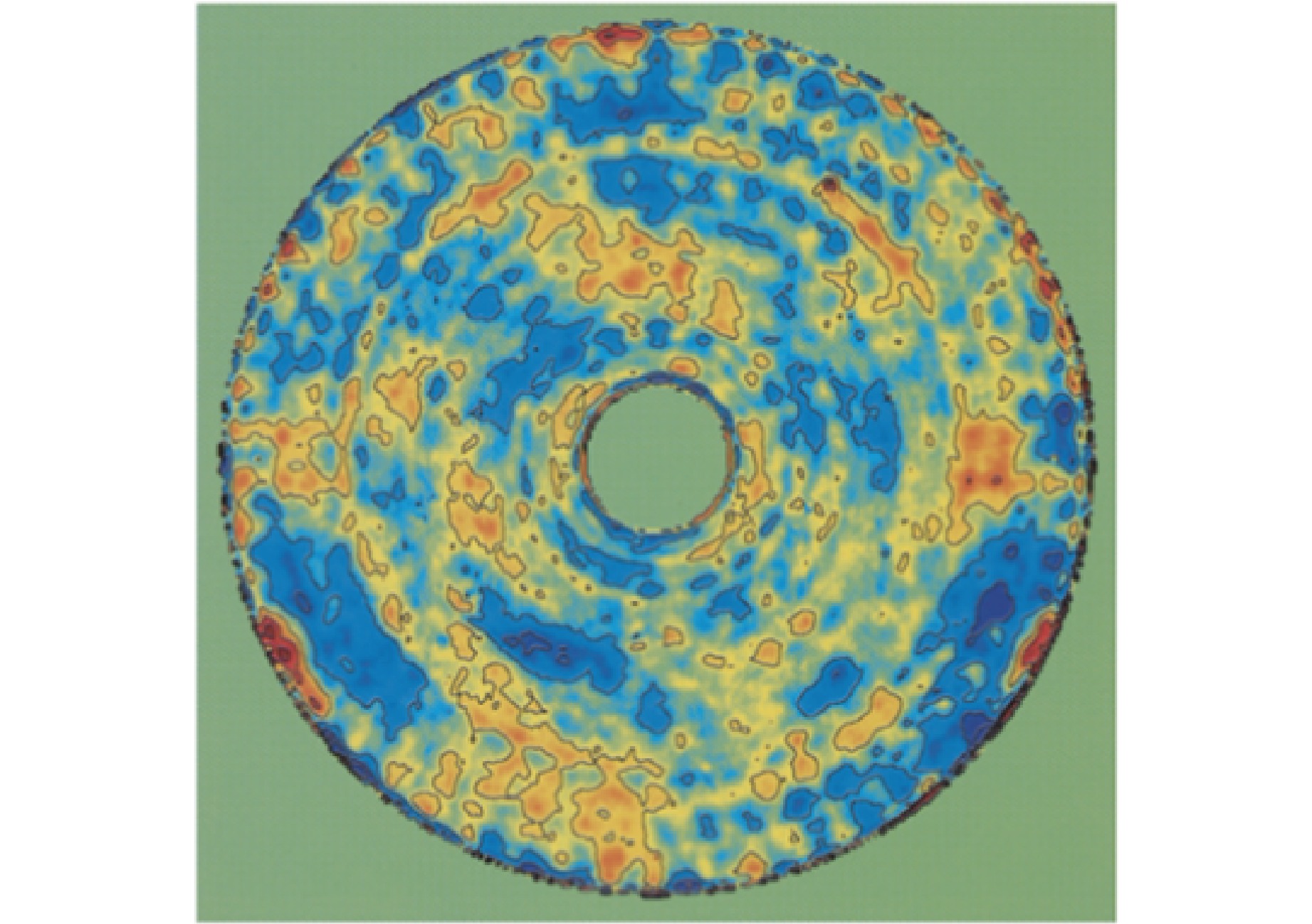
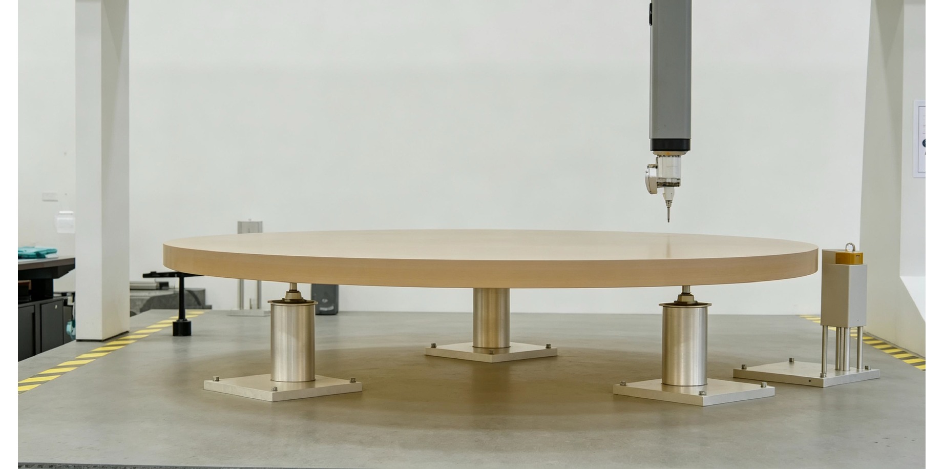
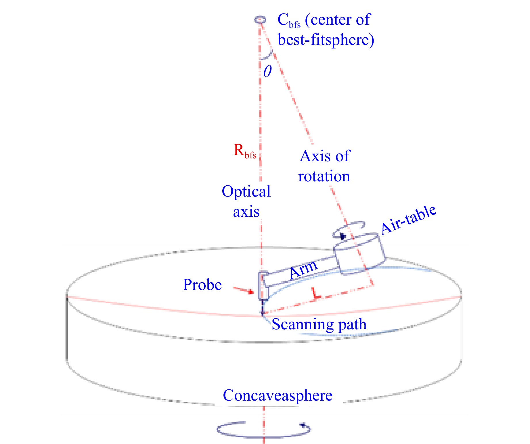
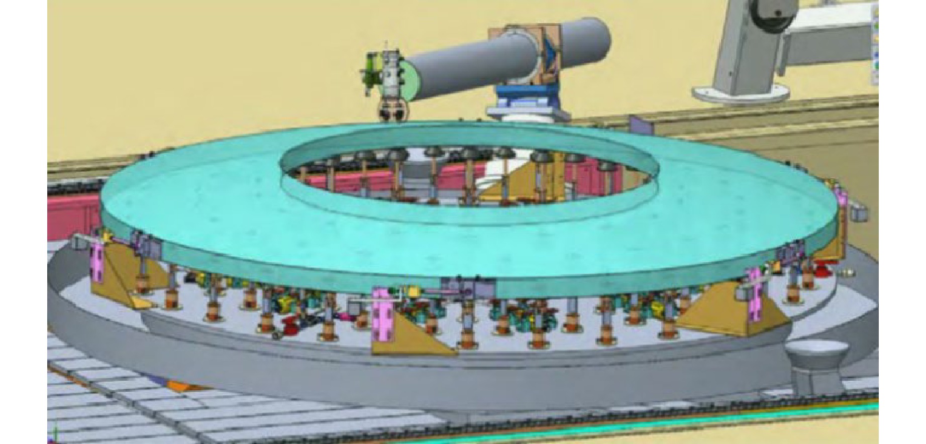
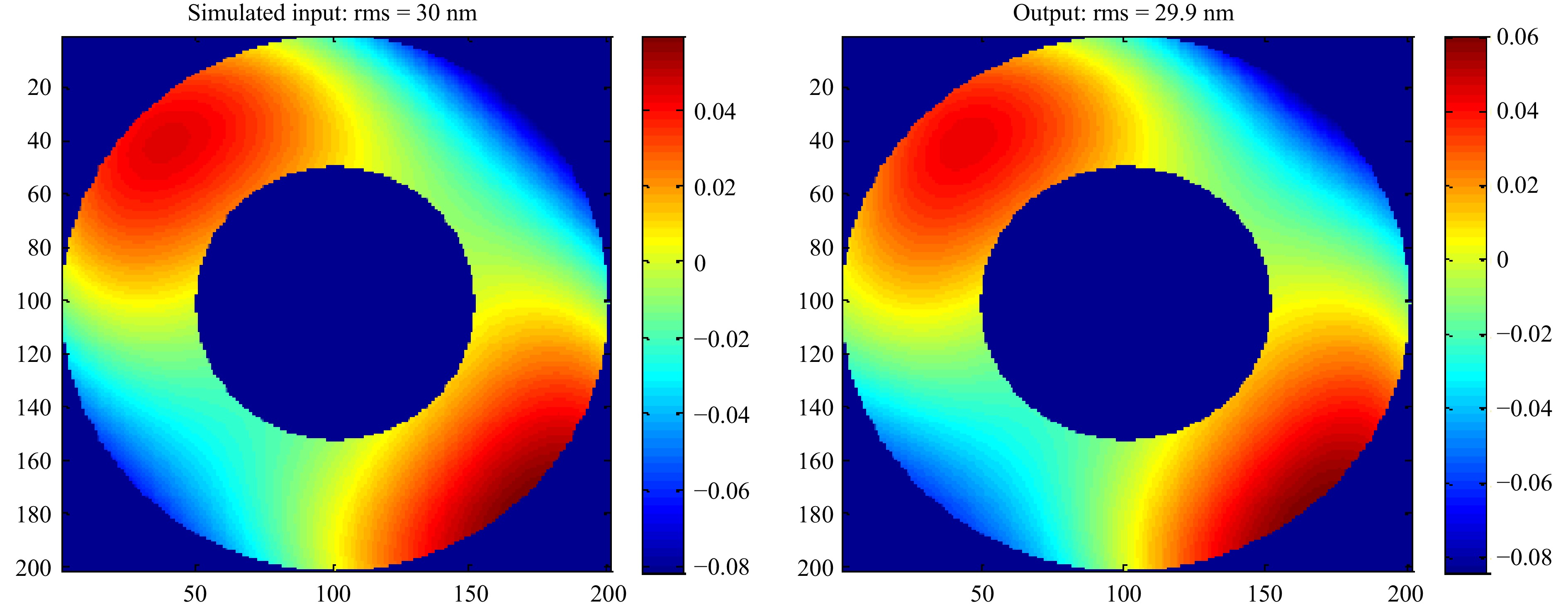
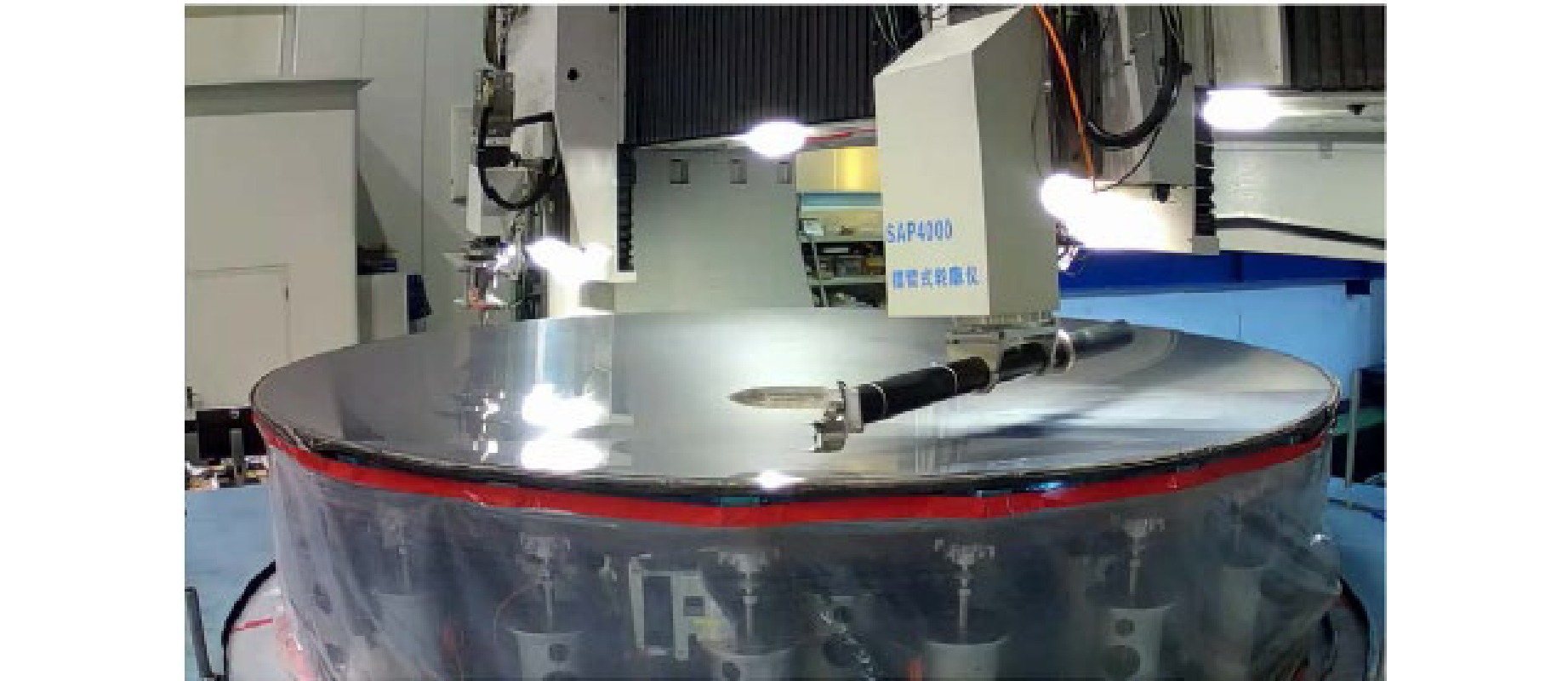
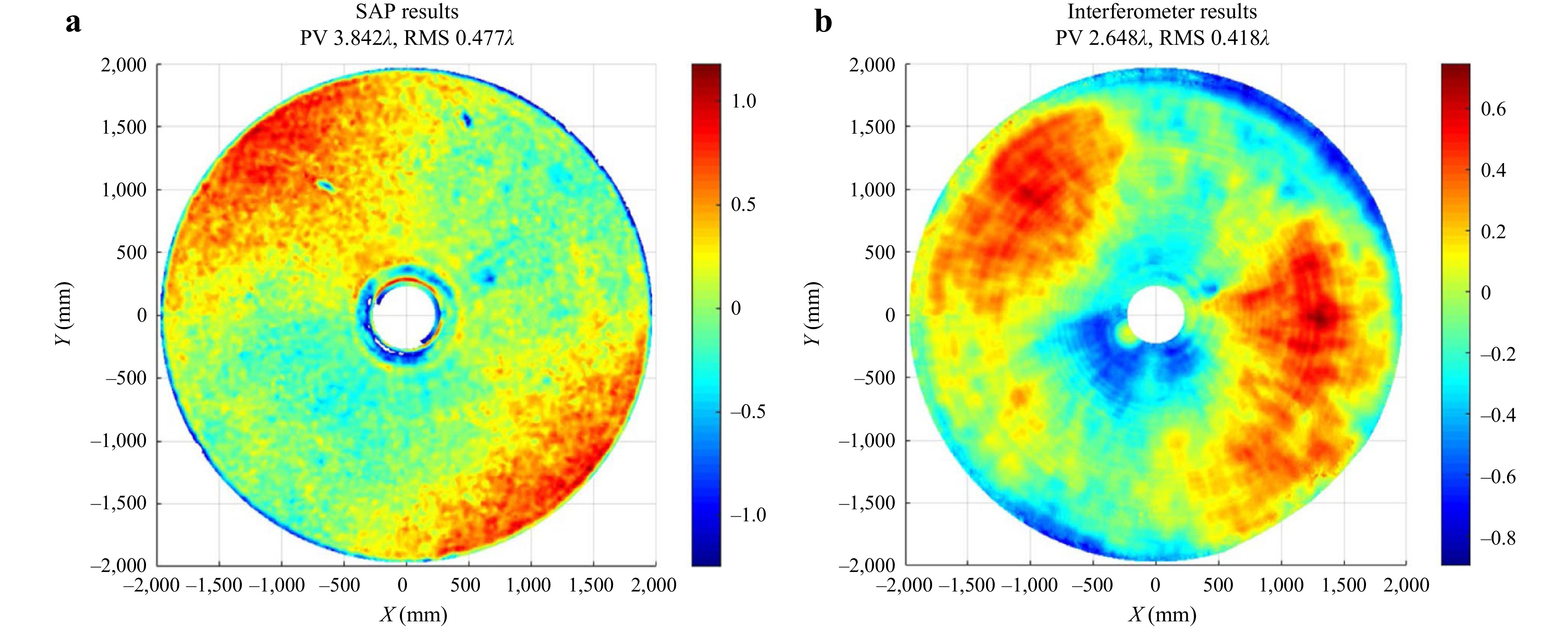
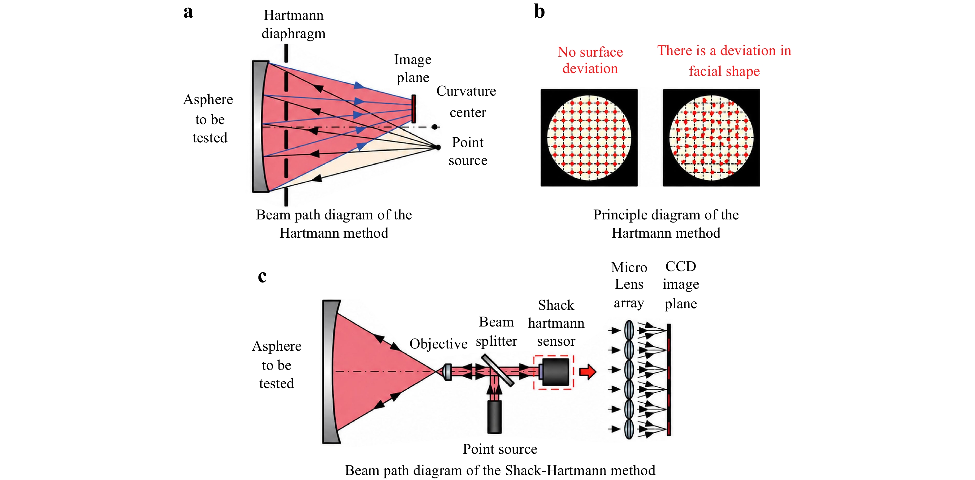
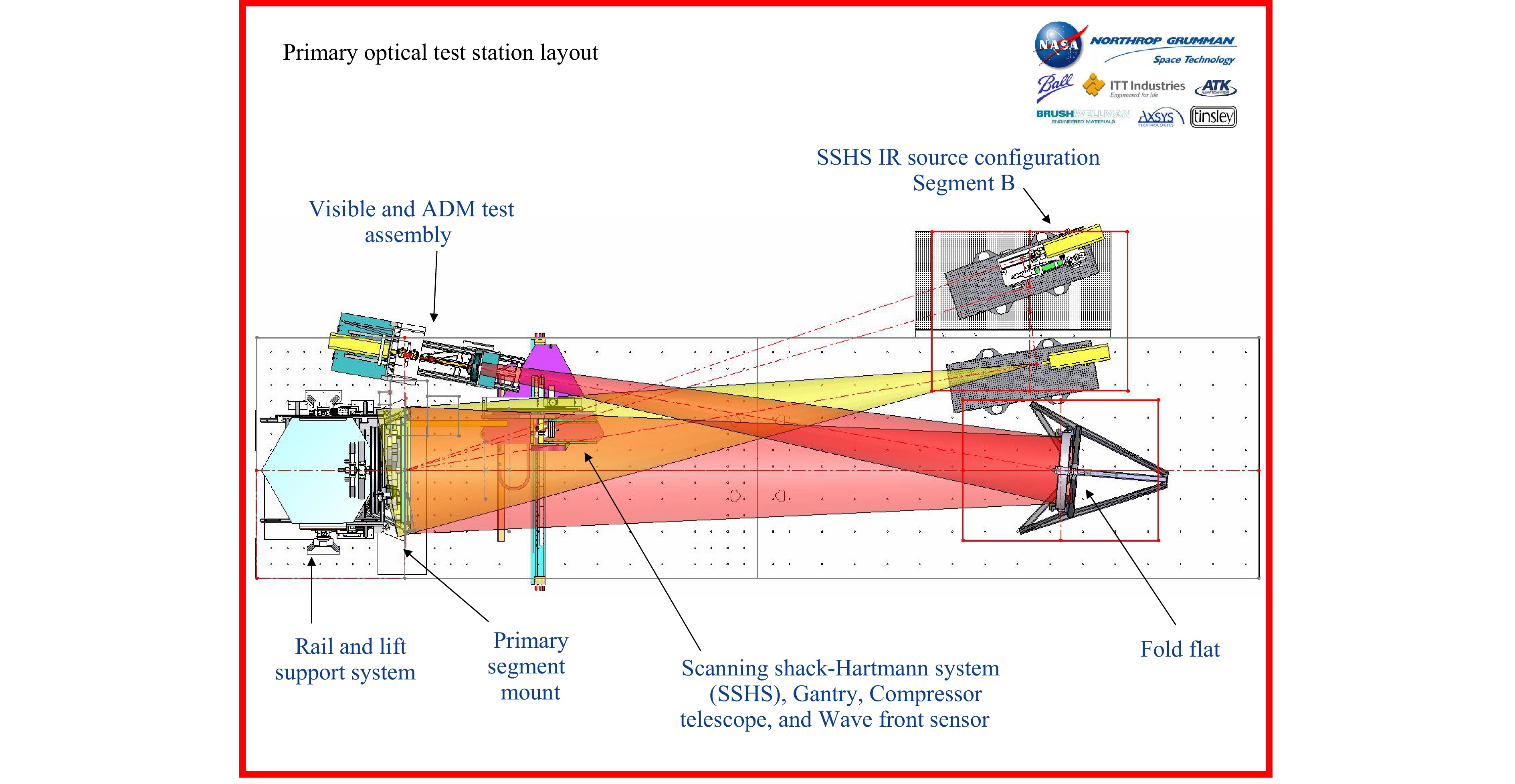
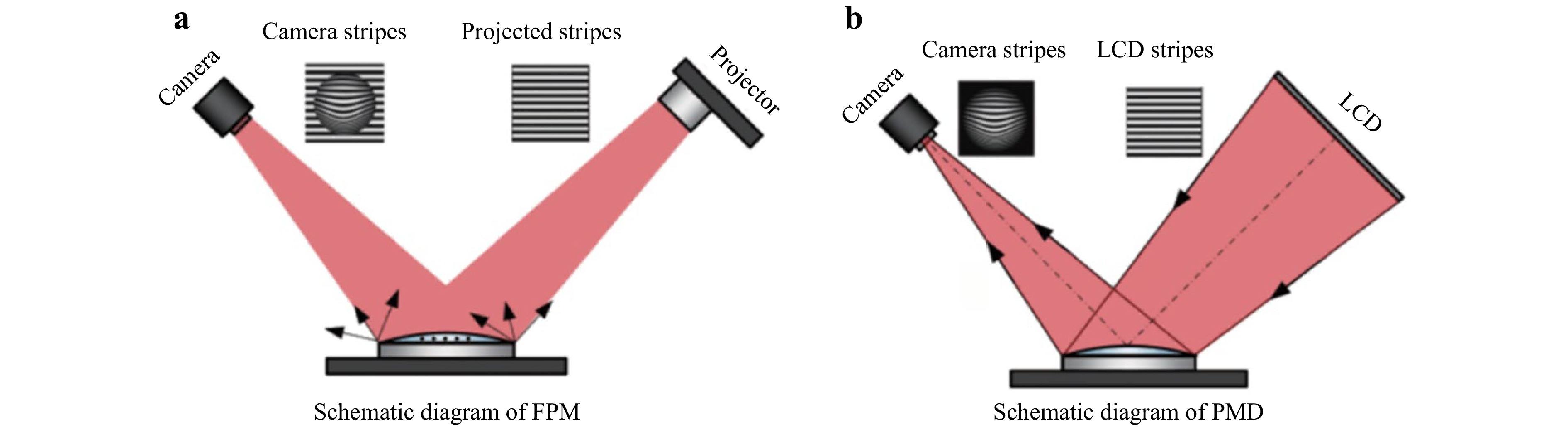
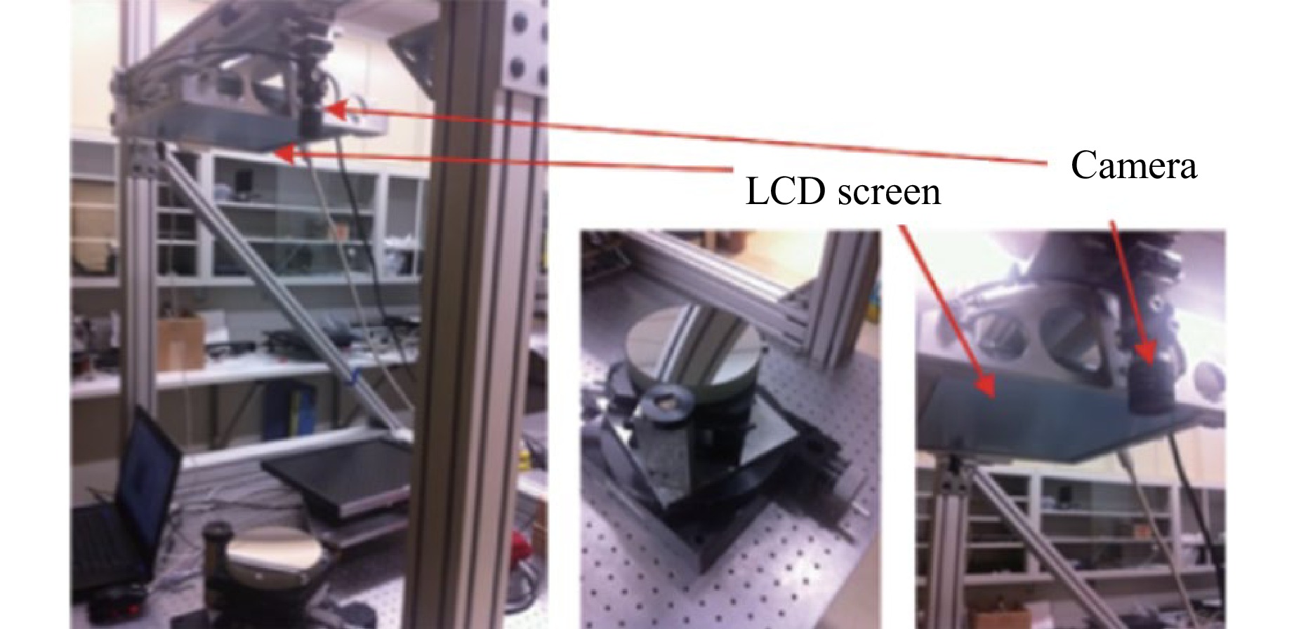
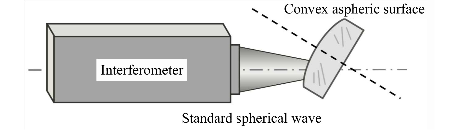
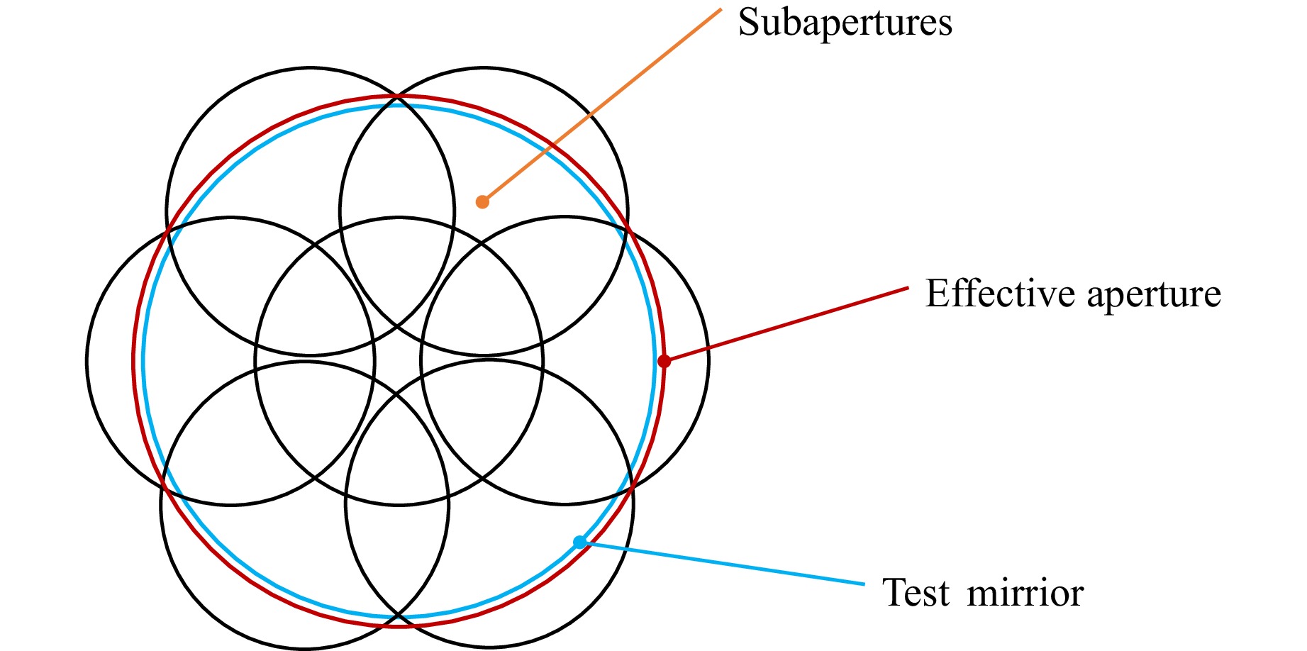
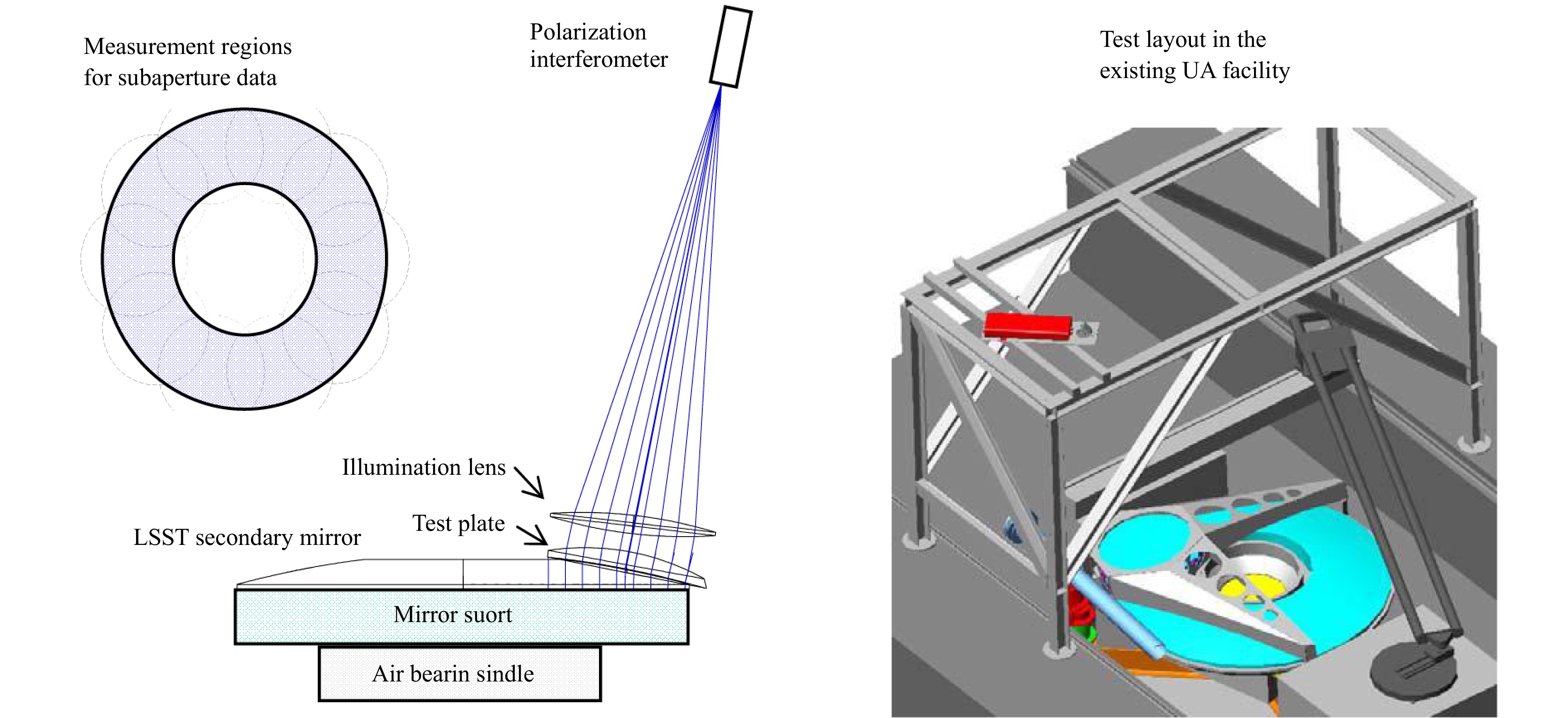
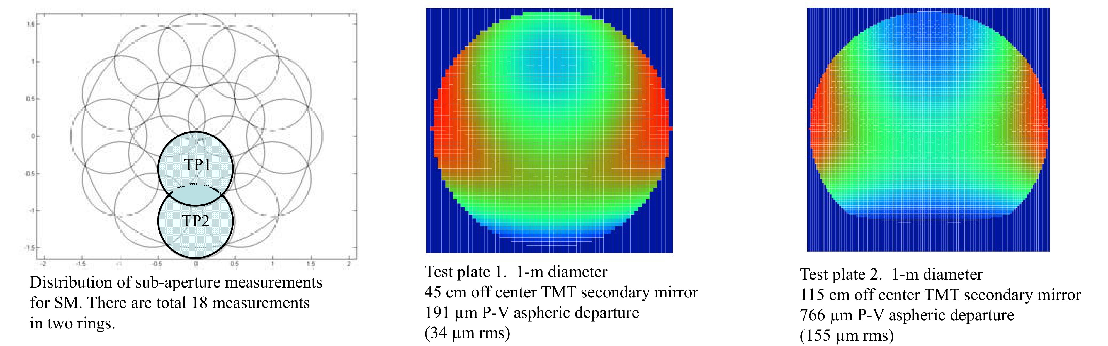
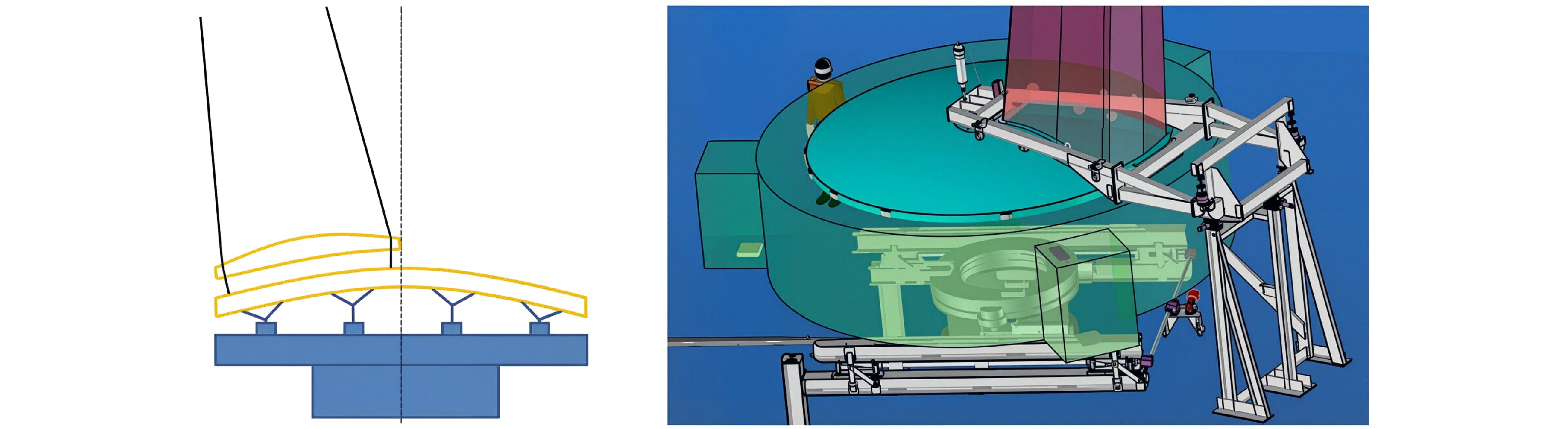
Large-aperture telescopes are indispensable tools for astronomical research. Over the past few decades, a host of representative projects have been developed, whose performance relies heavily on the manufacturing and testing technologies for large-aperture mirrors. This paper reviews the state-of-the-art fabrication and testing methods for large optical mirrors and is structured into five parts: application background, classification of manufacturing techniques, overview of metrology technologies, verification and standards, as well as conclusions and future perspectives. Sustained innovation in fabrication and testing lays a solid foundation for technological progress in this field and the implementation of next-generation telescope projects. Key development directions include achieving sub-nanometer-level surface accuracy, boosting large-batch manufacturing efficiency, upgrading metrology equipment and methodologies, and promoting the intelligent and automated integration in fabrication and metrology systems. It is expected that this review will serve as a valuable reference for researchers aiming to gain a full insight into understanding of manufacturing and testing technologies for large-aperture optical components.


Published. 2026, 7(3)
: 1024-1043
doi: 10.37188/lam.2026.077
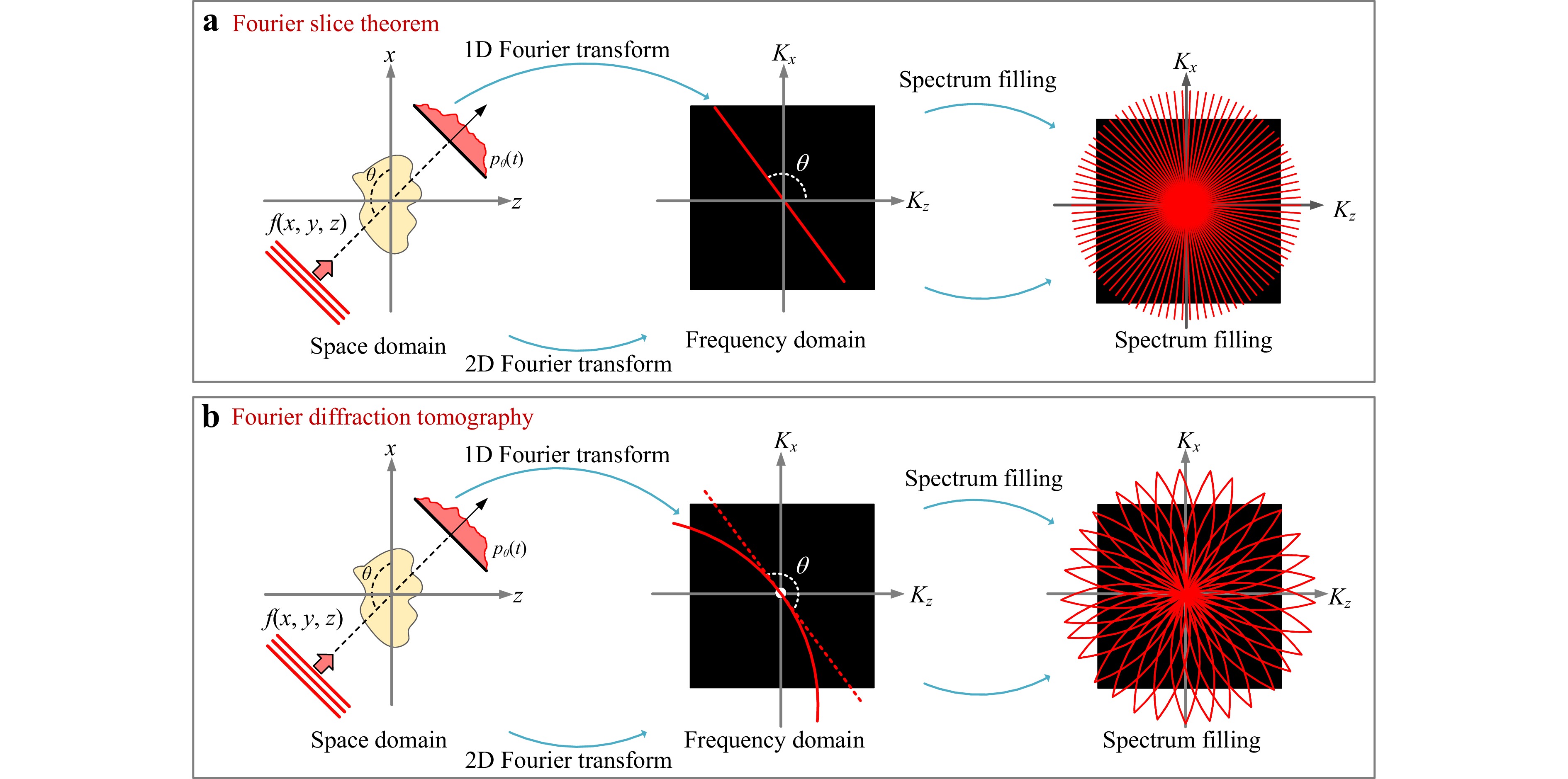
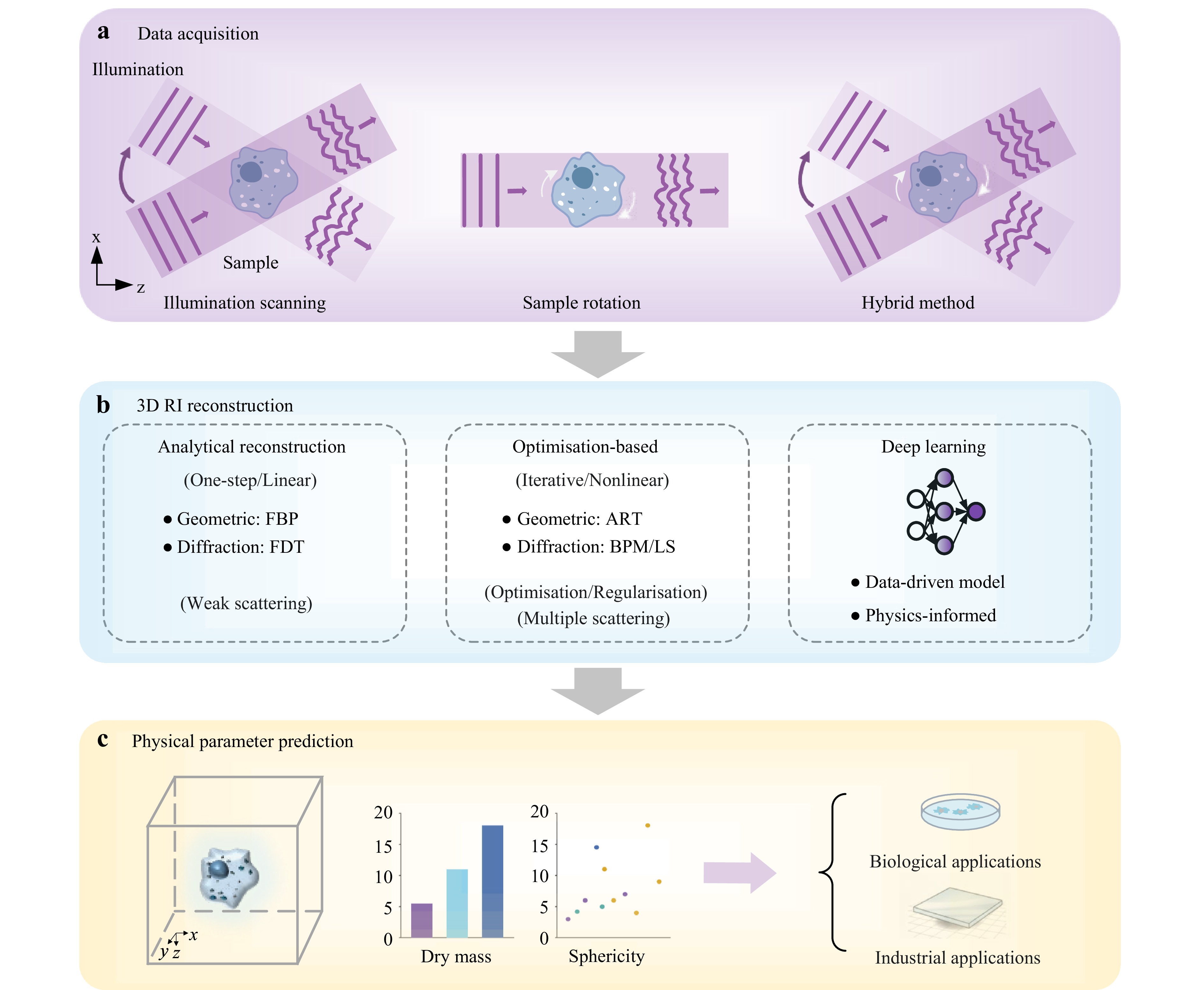
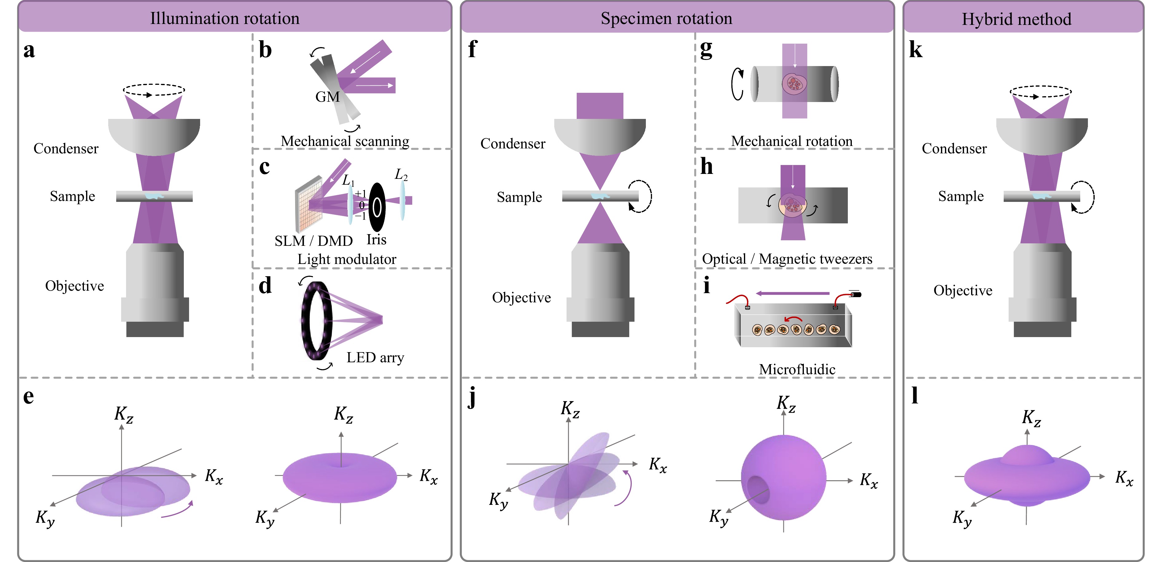
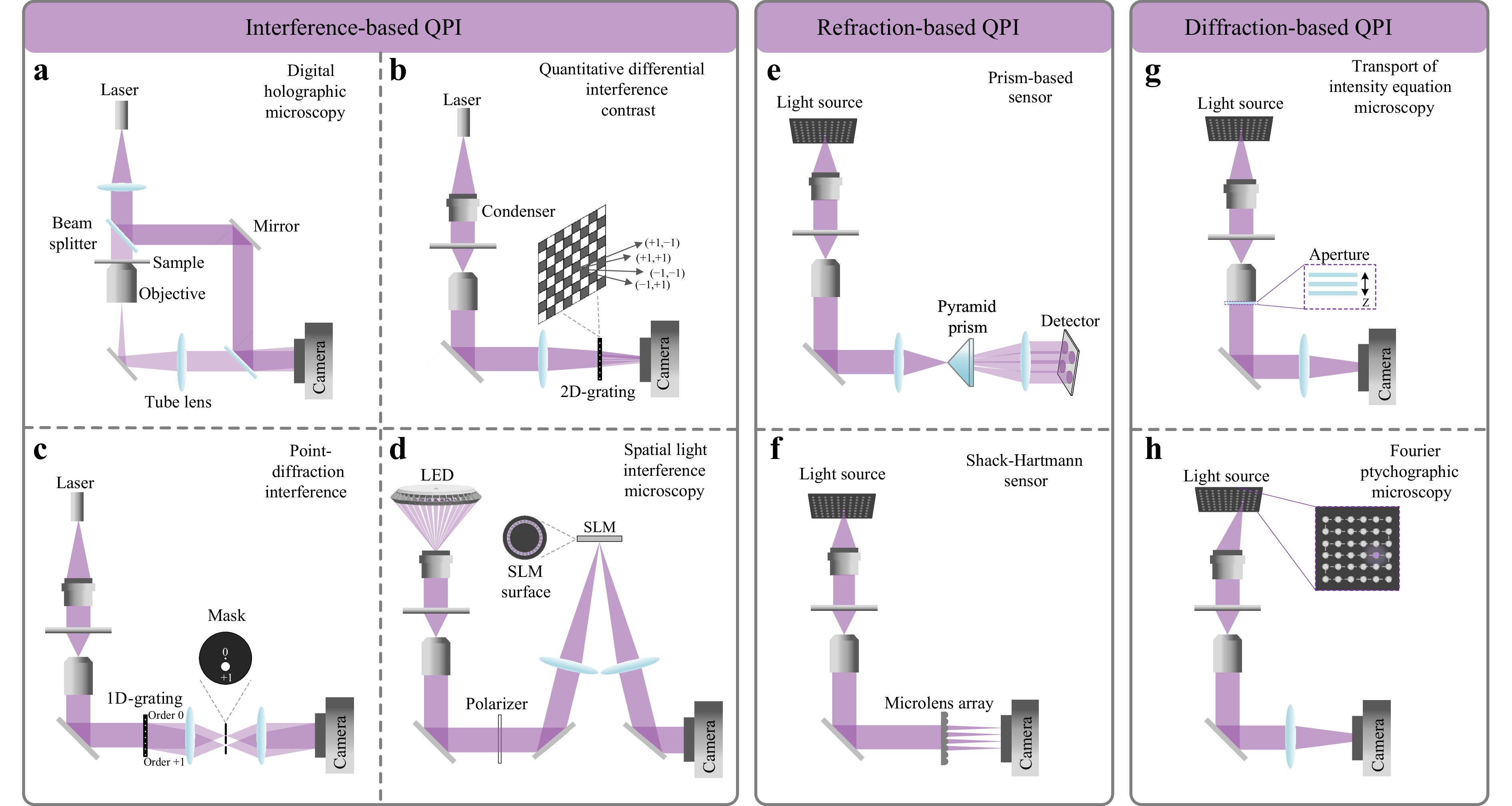
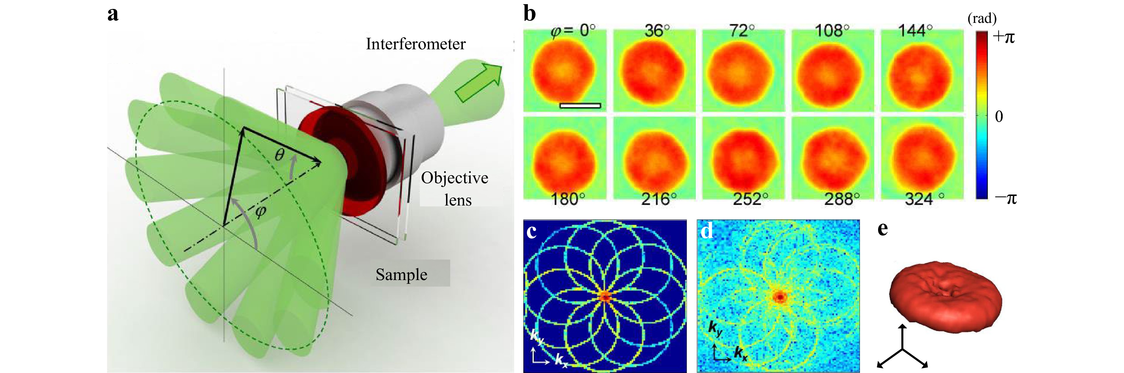
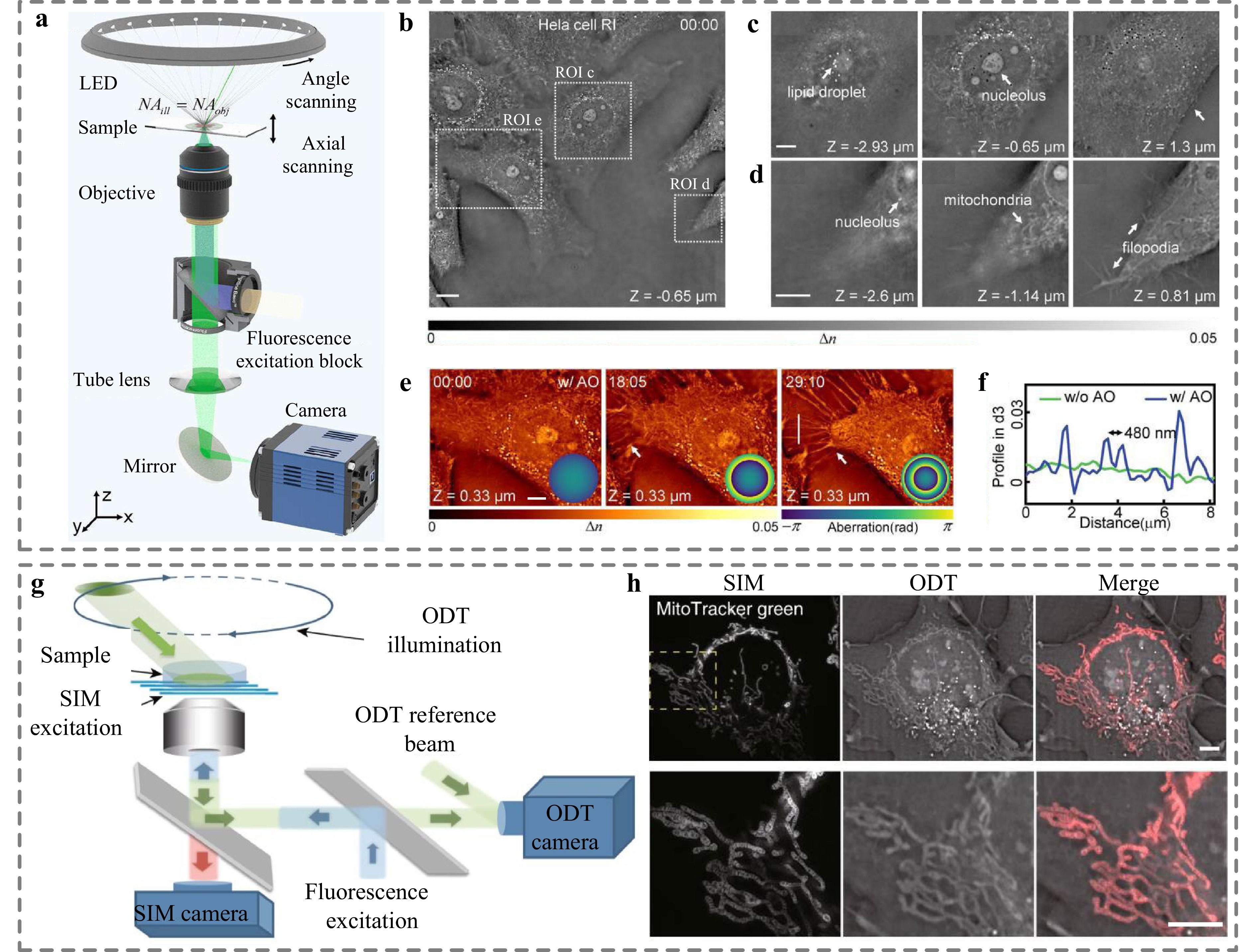
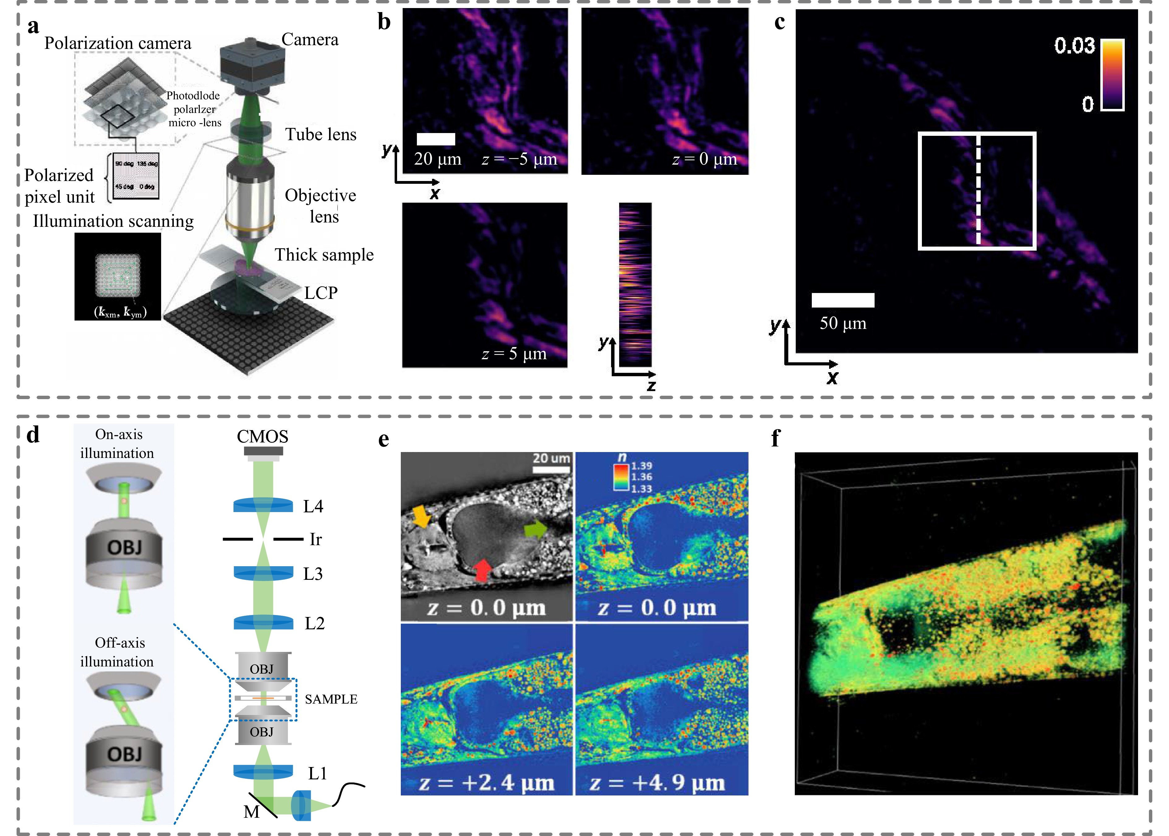
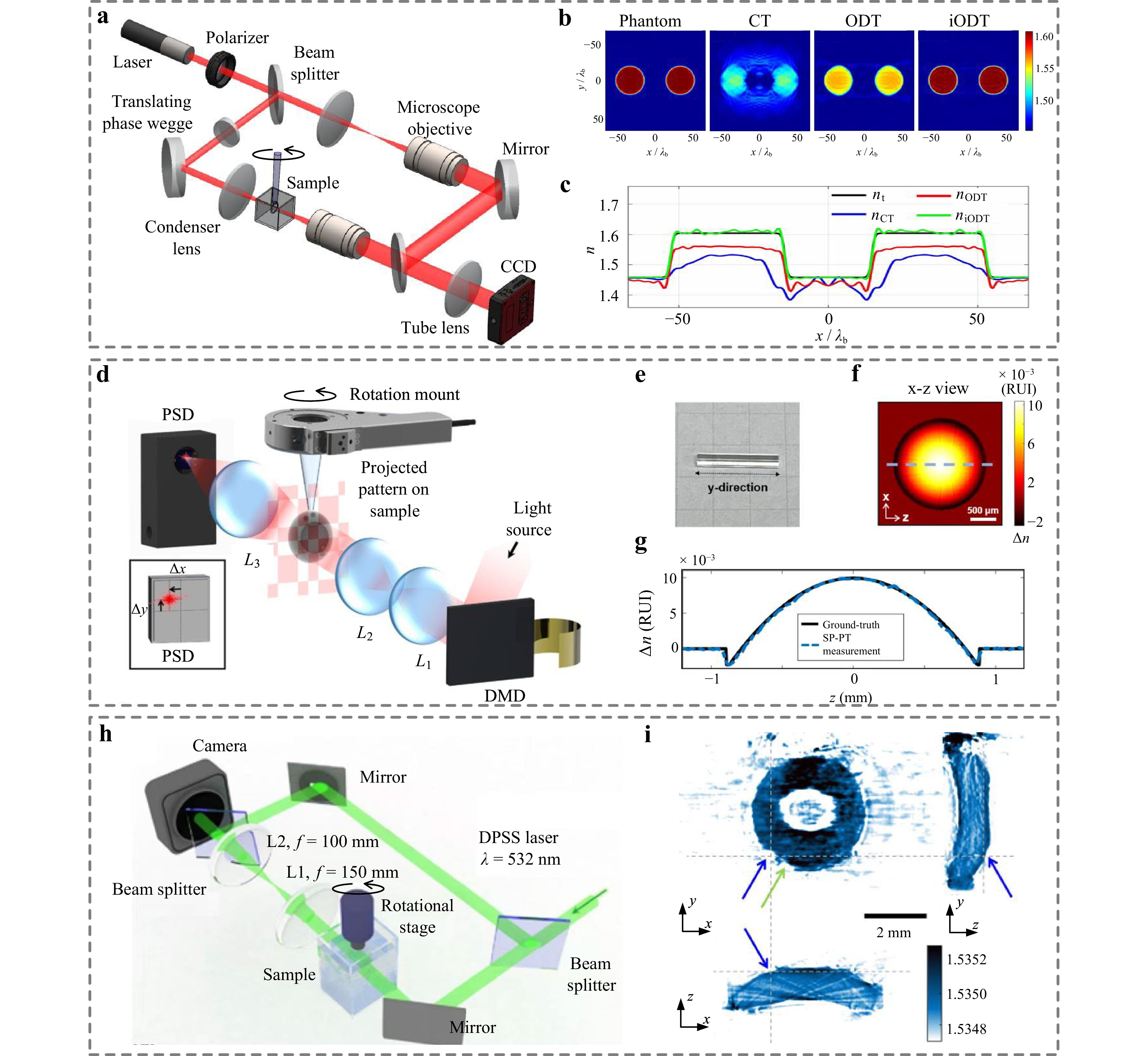
Refractive index (RI) is related to the physical parameters of a sample including morphology and tension. Consequently, three-dimensional RI imaging is critical for many fields. Three-dimensional (3D) RI imaging can be realised by recording transmittance wavefronts of a sample at different illumination angles and using the Fourier slicing or Fourier diffraction theorem to reconstruct the 3D RI image. Currently, advanced label-free 3D RI imaging techniques such as optical tomography and optical diffraction tomography have been increasingly utilised in many fields and demonstrated promising results. To further promote the application of 3D RI imaging technology, this paper provides an overview of the basic principles, experimental implementations, and applications of 3D RI imaging techniques. Further, the performance and characteristics of 3D RI imaging techniques with different illumination strategies and different reconstruction algorithms are compared, and the current trends and future perspectives are discussed. We hope that this review serves as a comprehensive guide to 3D RI imaging for both microscopists and biologists.
Published. 2026, 7(3)
: 1044-1074
doi: 10.37188/lam.2026.078
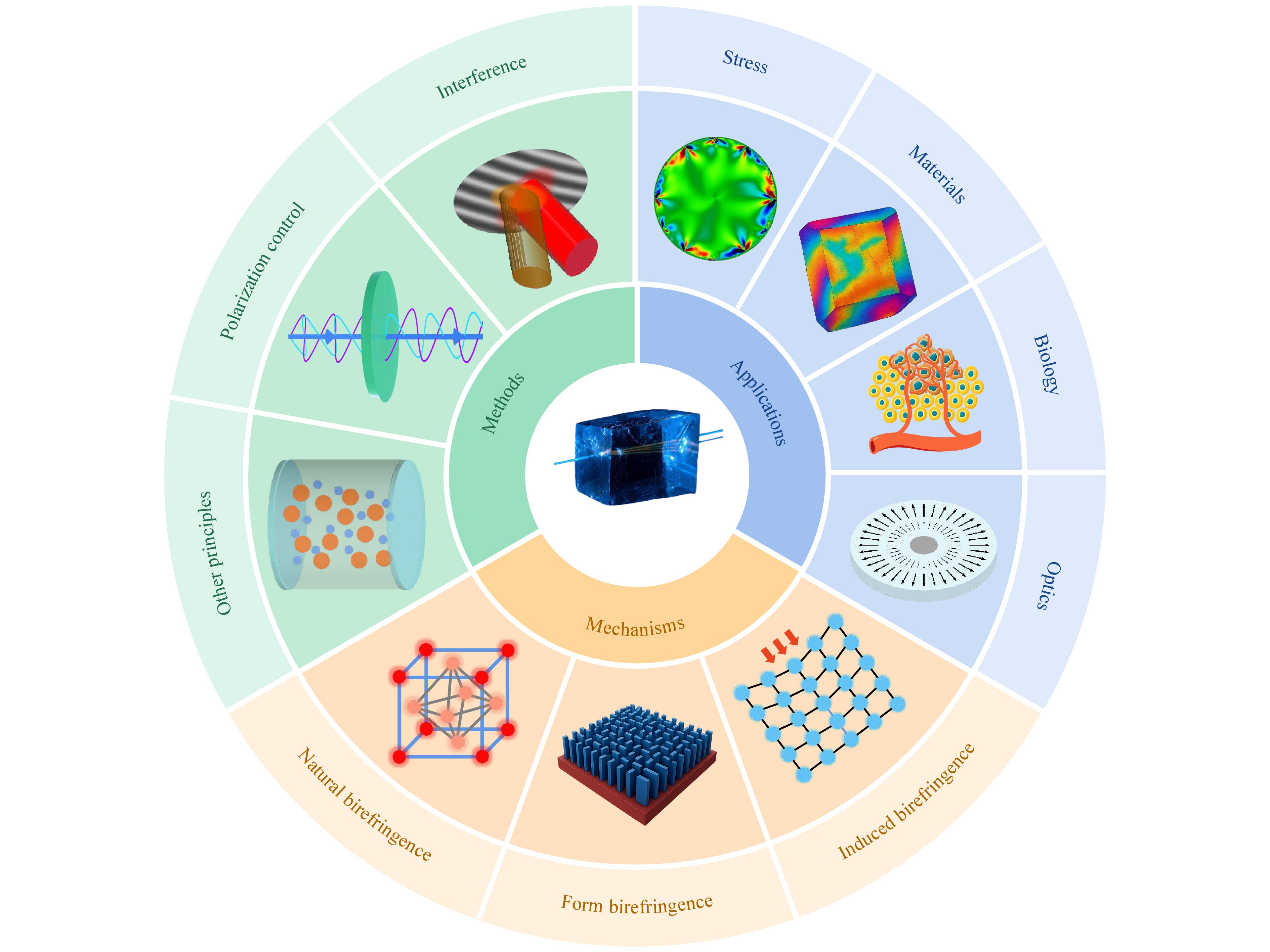
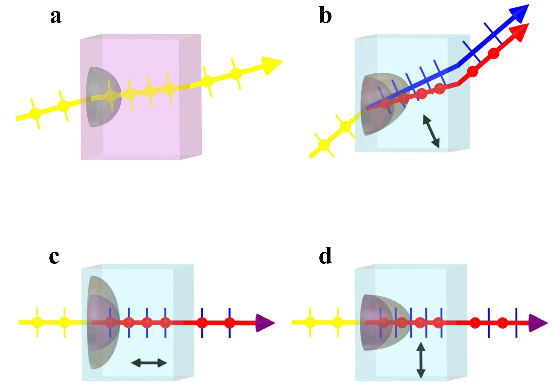
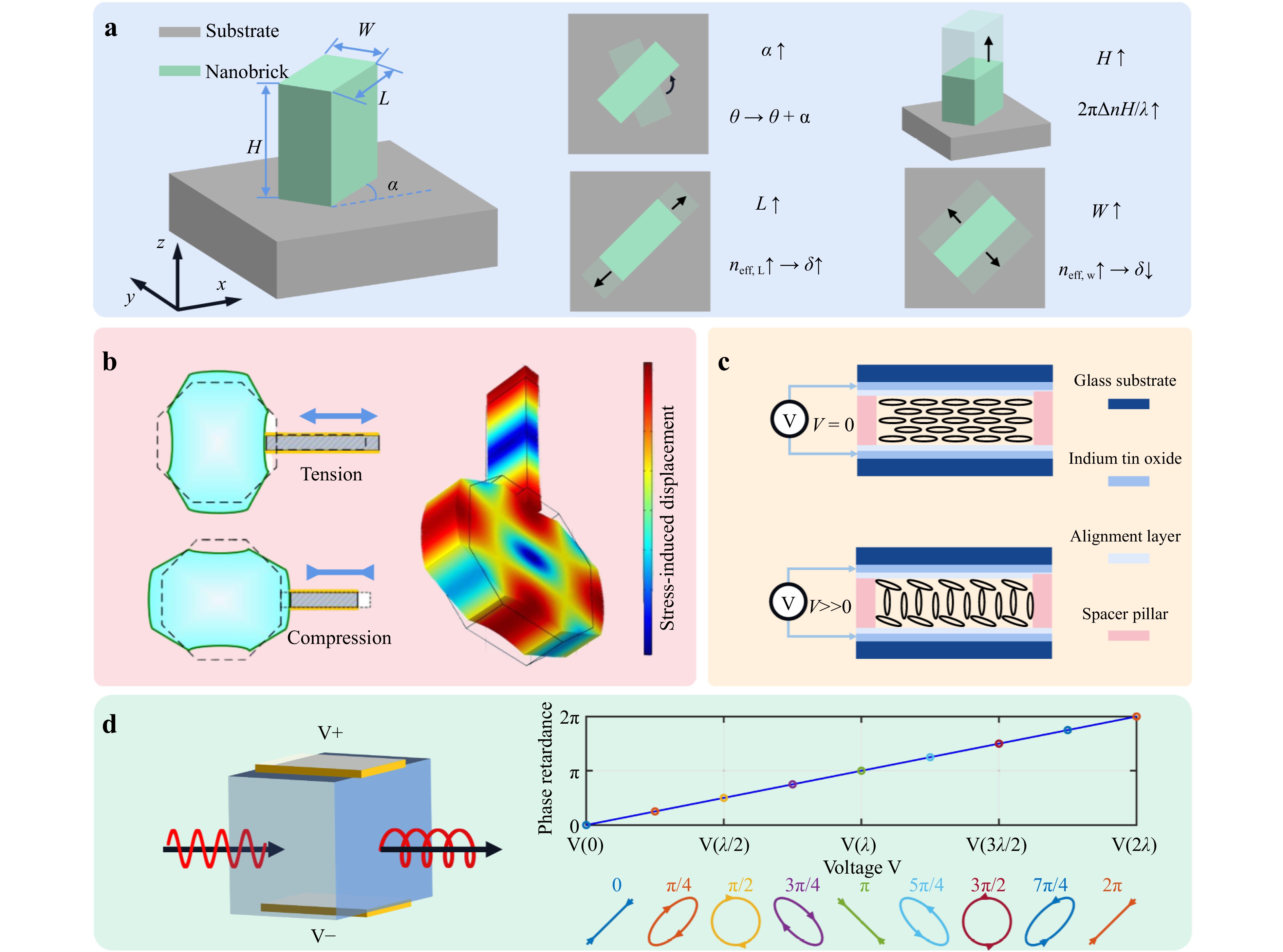
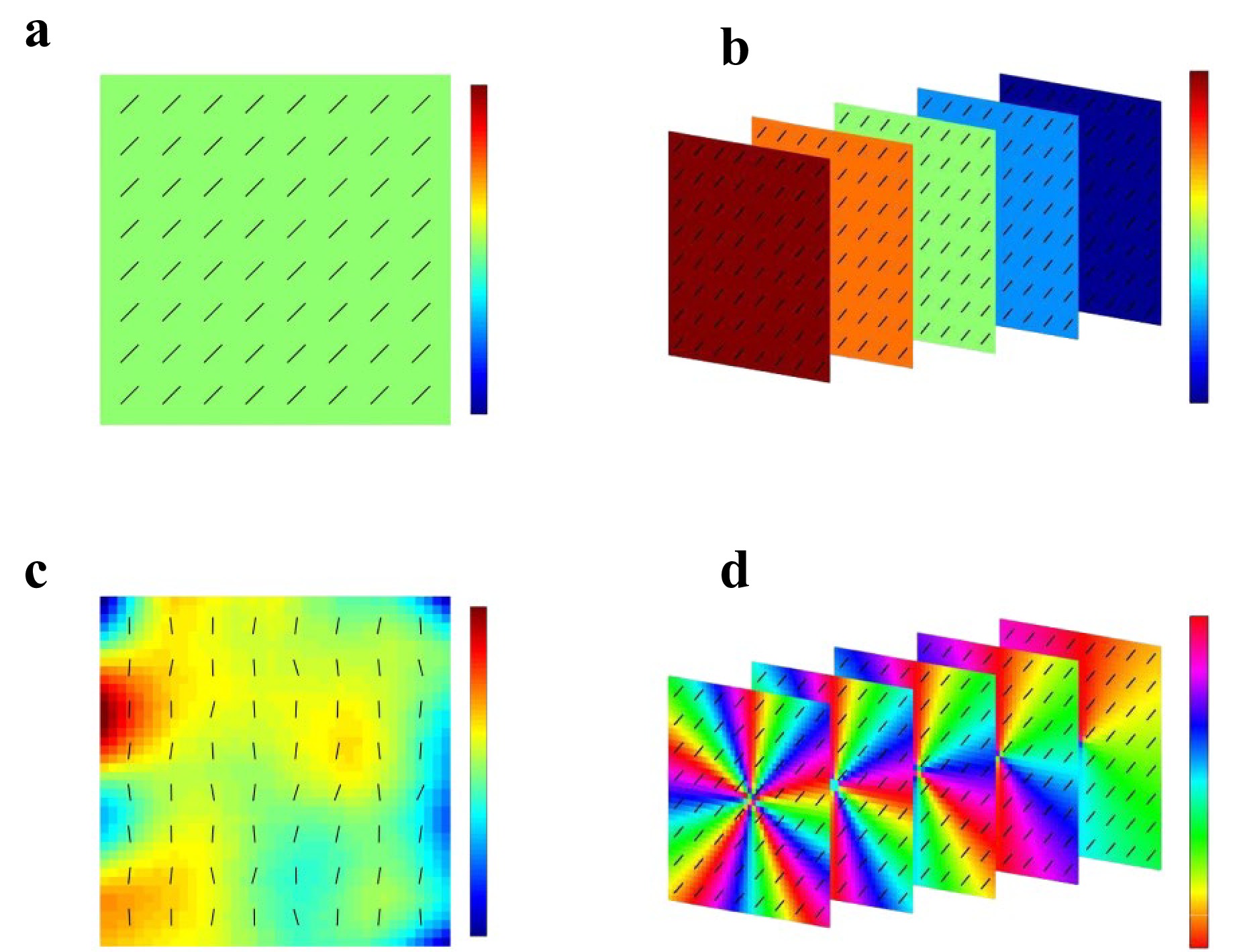
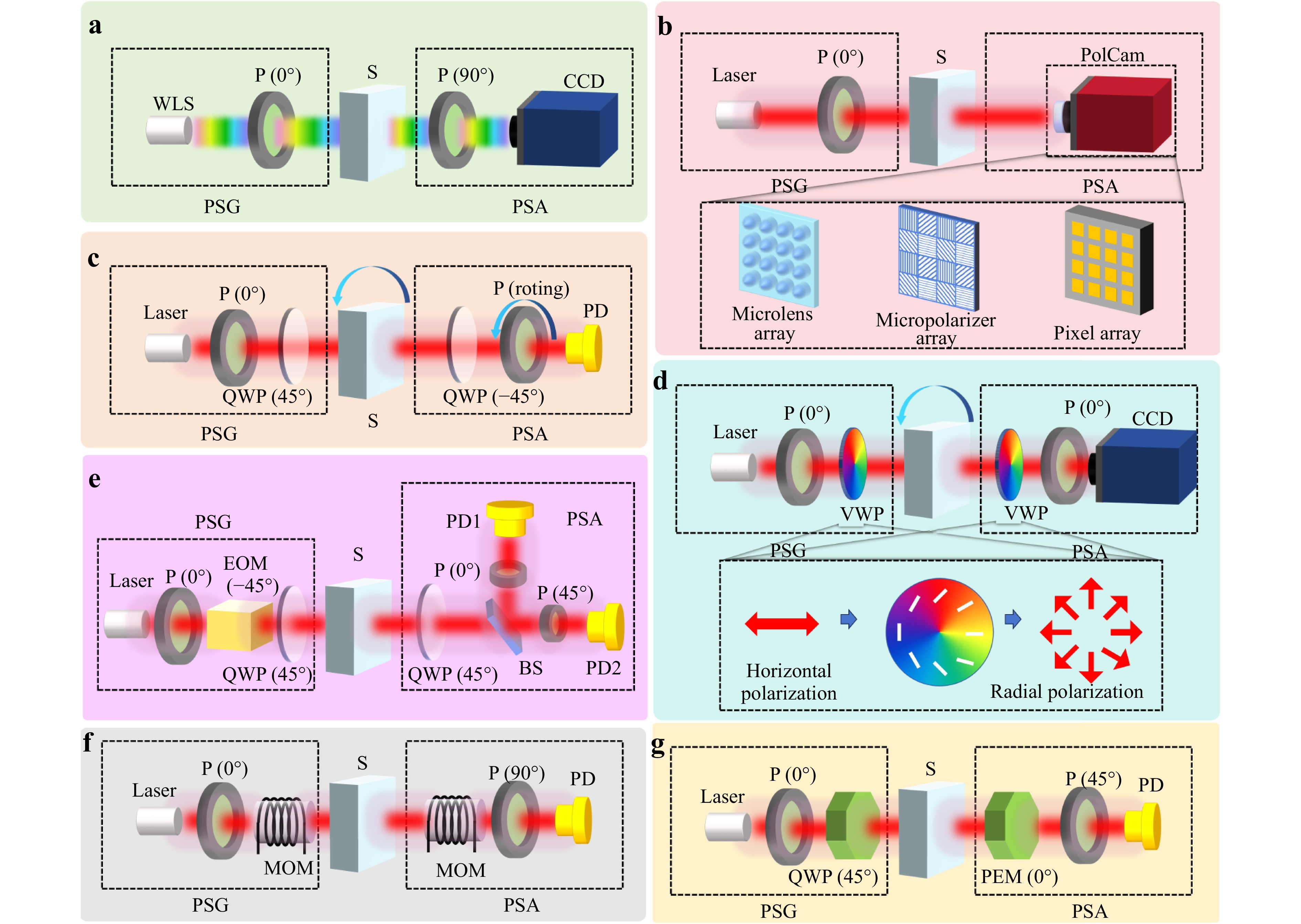
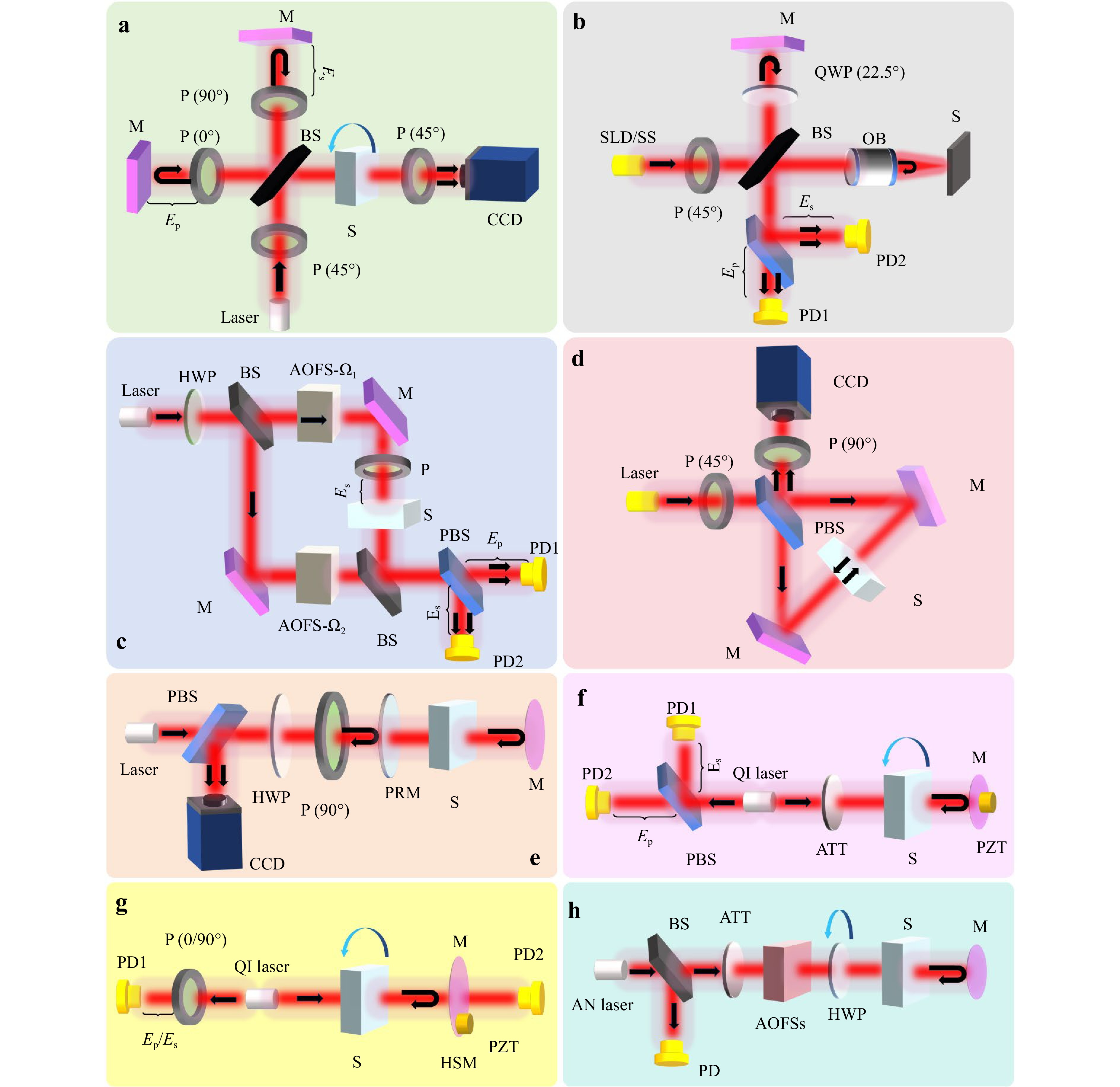
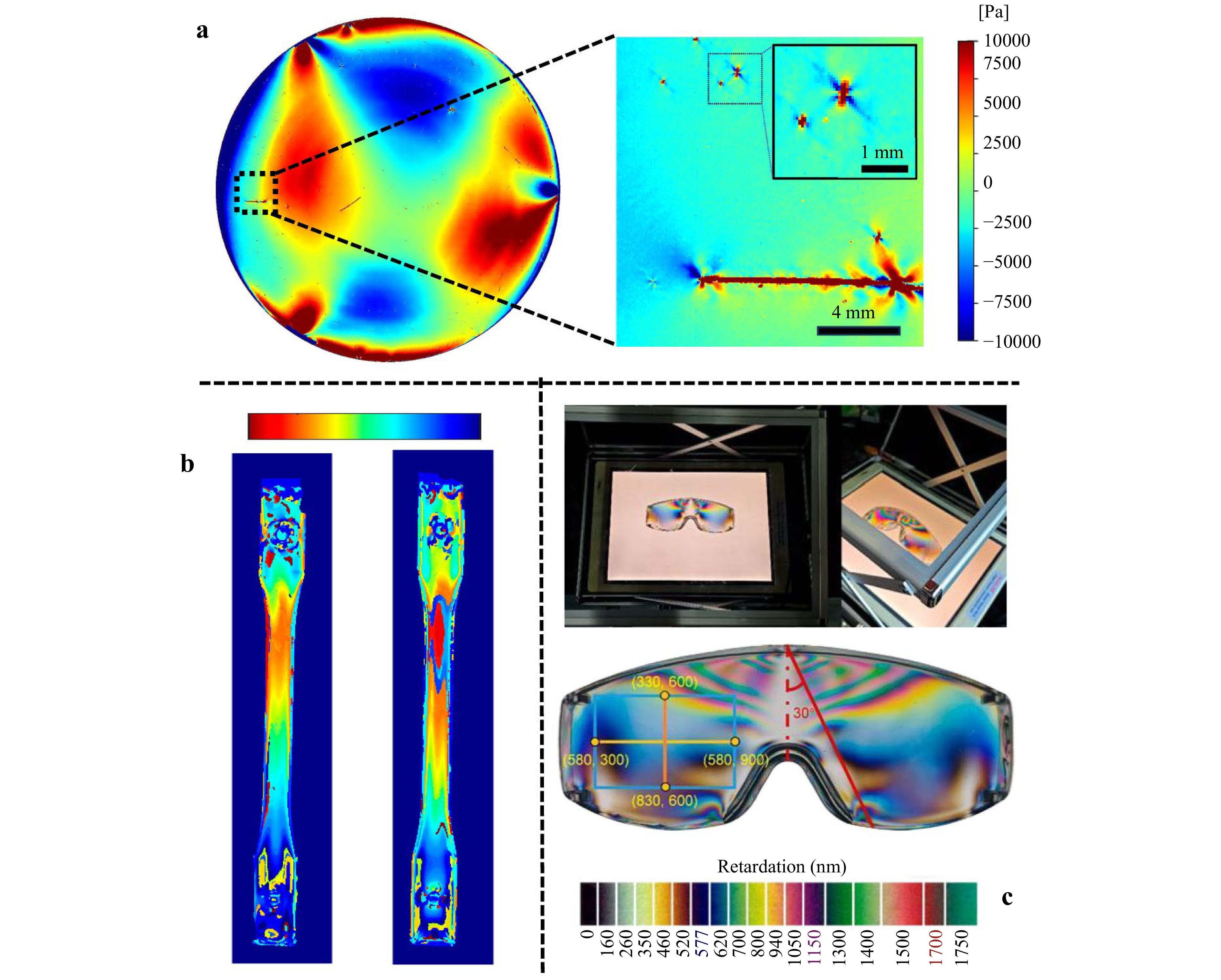
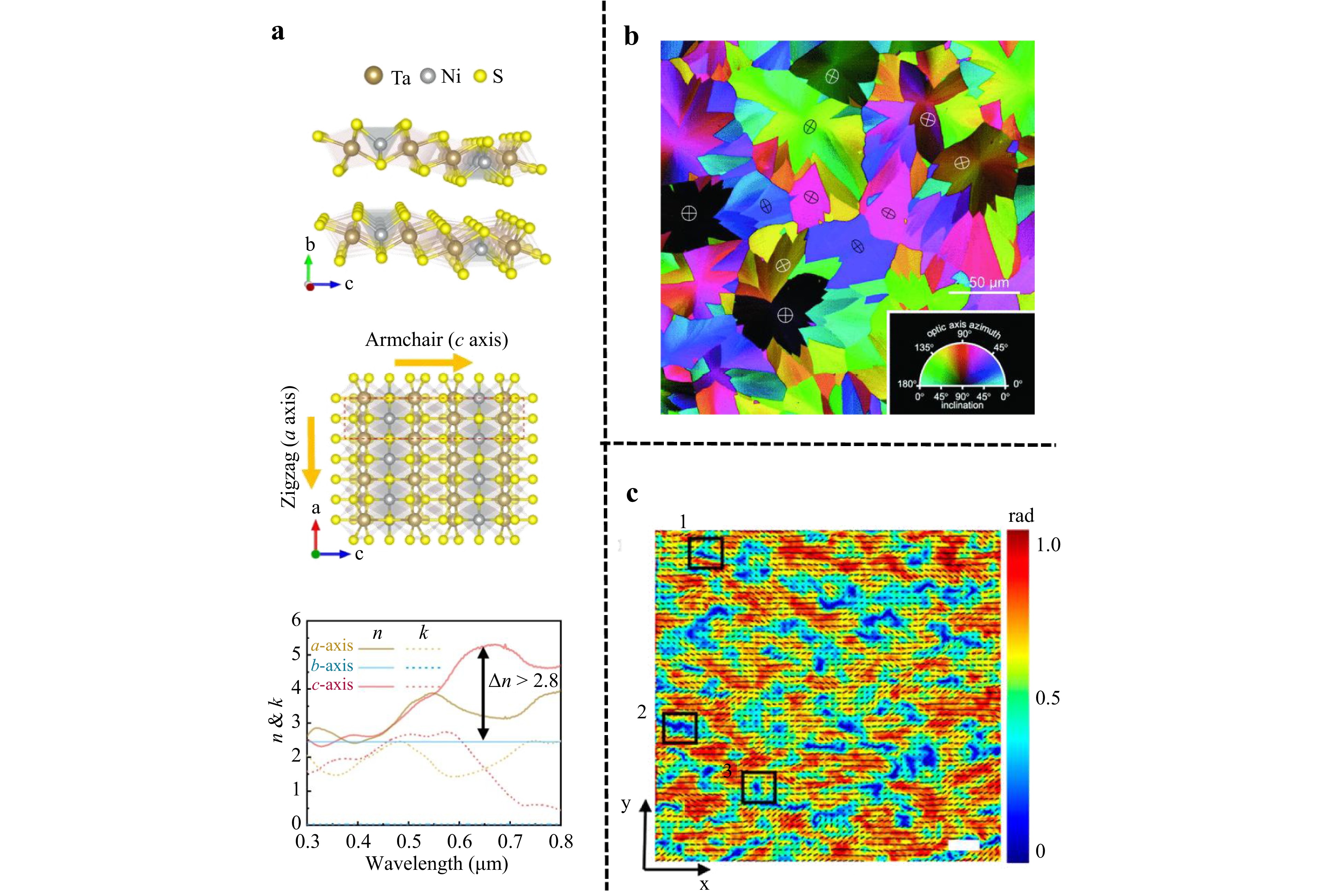
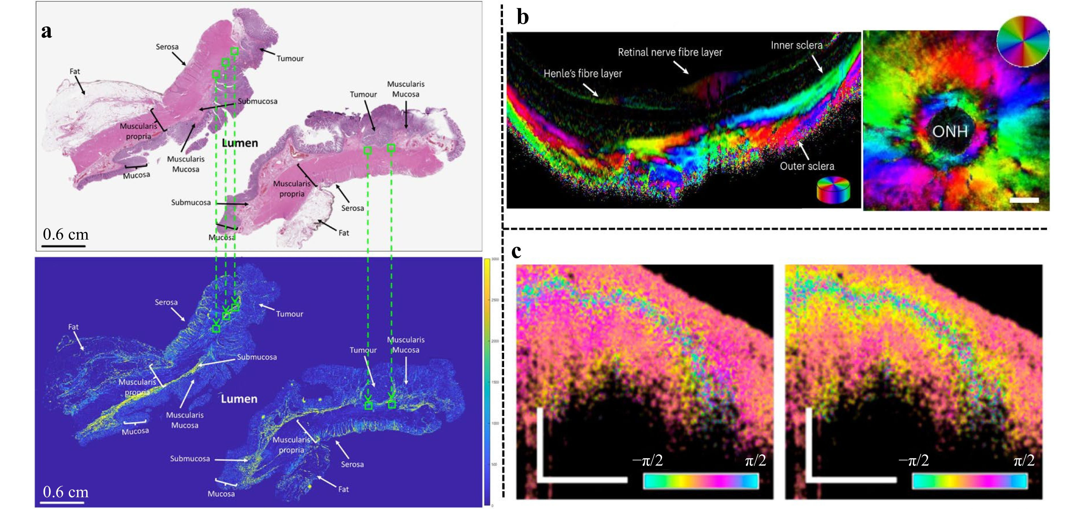
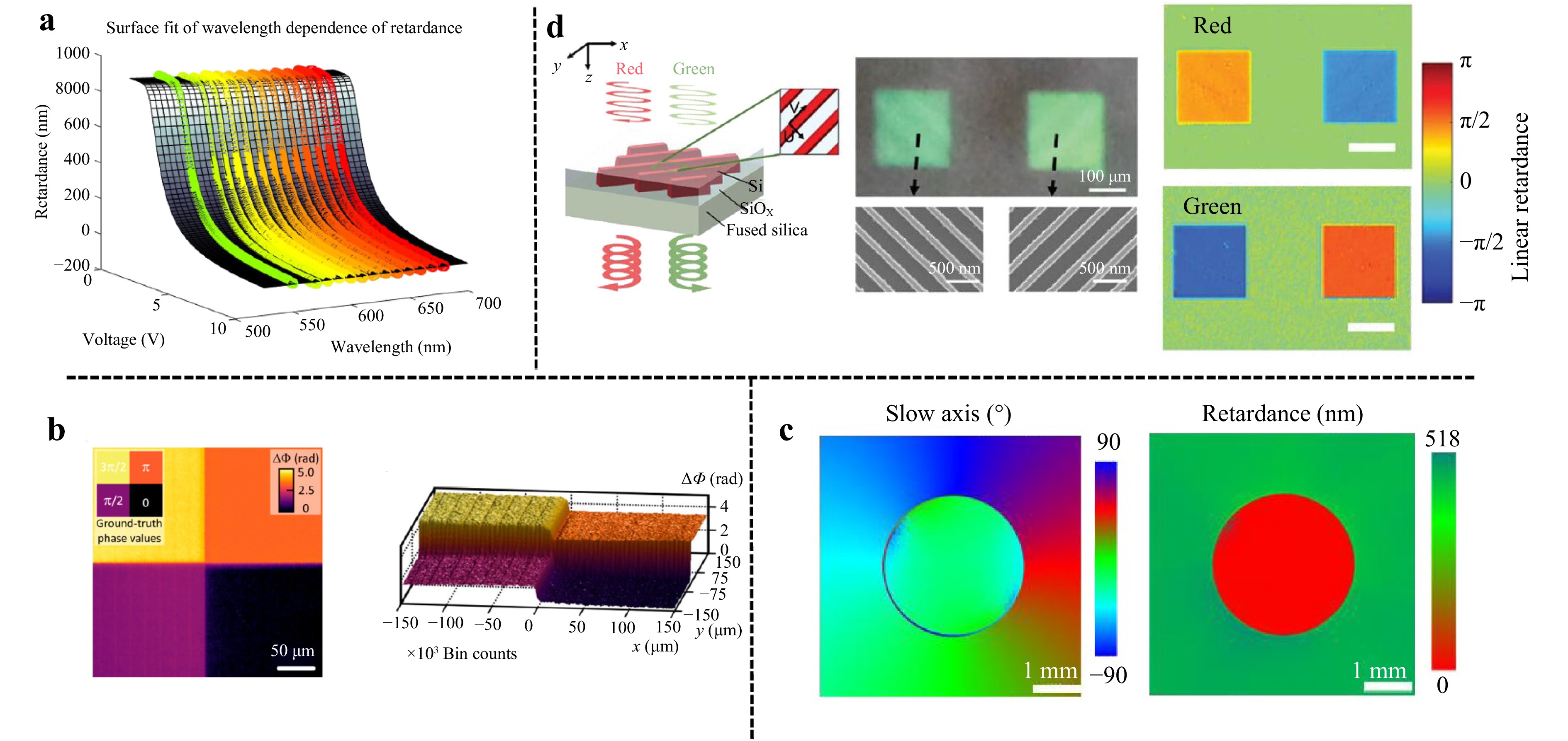
Birefringence refers to the optical anisotropy of transparent media, manifesting as light-wave splitting and phase differences owing to the direction-dependent refractive indices. This phenomenon is closely related to the internal microstructure, stress state, and external fields that affect materials. In recent years, birefringence analysis has gained increasing attention as a powerful tool for revealing the microscopic anisotropic features, polarisation responses, and macroscopic stresses that are difficult to observe using conventional methods. The accurate measurement and characterisation of birefringence in transparent media have become critical in fields such as materials science, biomedicine, and precision manufacturing. This paper provides a comprehensive review of the methods used for birefringence measurement based on polarisation optics. First, it introduces the birefringent polarisation optical theory, mechanisms of birefringence, and classification of the measurement characteristics. Subsequently, common techniques including polarisation modulation analysis, interferometric methods, and other optical approaches are presented in detail, covering their principles, features, advantages, limitations, and applicable scenarios. Recent research advances are also discussed, with an emphasis on applications such as residual stress analysis, characterisation of advanced material anisotropy, pathological diagnosis in biological tissues, and performance evaluation of novel birefringent components. Finally, current challenges are outlined, and future trends in the field are proposed.


 Email
Email RSS
RSS